

Page 1
MITSUBISHI Dig./Ana.INTERFACE
PRELIMINARY
PRELIMINARY
Notice:This is not a final specification.
Some parametric limits are subject to change.
GENERAL DESCRIPTION
The M62703ML/SL is a voltage threshold detector designed
for detection of a supply voltage and generation of a system
reset pulse for almost all logic circuits such as
microcontroller.
It has extensive applications including battery checking, level
detecting and waveform shaping circuits.
FEATURES
• Few external components
• Low operating threshold voltage (Supply voltage to keep a
output low in a low supply operation)
…0.65V(typ) at RL = 22kΩ
• Wide supply voltage range ………… 2V to 7V
• High immunity to a sudden supply voltage change
• Wide application range
• Extra small 3-pin package (3-pin FLAT)
APPLICATION
• Reset pulse generation for almost all logic circuits
• Battery checking, level detecting, waveform shaping circuits
• Delayed waveform generating circuit
• Switching circuit to a back-up power supply
• DC/DC converter
• Over voltage protection circuit
VOLTAGE DETECTING, SYSTEM RESETTING IC SERIES
M62703ML,SL
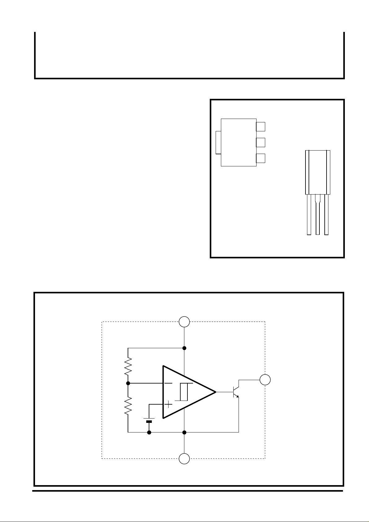
PIN CONFIGURATION (TOP VIEW)
3
OUTPUT
GND
2
M62703ML
Outline SOT-89
SUPPLY
1
VOLTAGE
(1) SUPPLY
VOLTAGE
(2) GND
(3) OUTPUT
(1) (2)(3)
Outline TO-92L
M62703SL
RECOMMENDED OPERATING CONDITION
• Supply voltage range ………… 2V to 7V
BLOCK DIAGRAM
SUPPLY VOLTAGE
R1
R2
1.25V
1
3 OUTPUT
2
GND
( / 3 )
1
Page 2
MITSUBISHI Dig./Ana.INTERFACE
PRELIMINARY
PRELIMINARY
Notice:This is not a final specification.
Some parametric limits are subject to change.
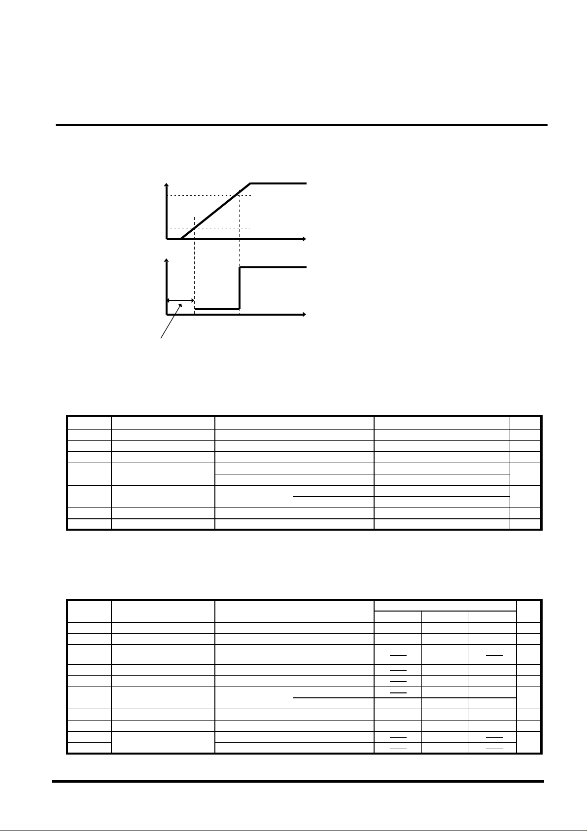
FUNCTION DIAGRAM
SUPPLY
VOLTAGE
2.87V
0.65V
OUTPUT
STATE
H
L
OUTPUT
UNDEFINED
M62703ML,SL
VOLTAGE DETECTING, SYSTEM RESETTING IC SERIES
ABSOLUTE MAXIMUM RATINGS (Ta=25°C, Unless otherwise noted)
Symbol Parameter Test condition Ratings Unit
ICC
Isink
VO
Pd
K
0-
Topr
Tstg
Supply Voltage
Output Sink Current
Output Voltage
Power Dissipation
Thermal Derating
Operating Temperature
Storage Temperature
Output with constant current load
3pin SIL
3pin FLAT
Ta≥25°C
3PIN SIL
3PIN FLAT
7
6
VCC
700
500
7
5
-30 to +85
-40 to +125
ELECTRICAL CHARACTERISTICS (Ta=25°C, Unless otherwise noted)
Symbol
VS
∆VS
VS/∆T
ICC
Vsat
VOPL
IOC
VOH
tPHL
tPLH
Parameter Test condition
Detecting Voltage
Hysteresis Voltage
Detecting Voltage
Temperature Coefficient
Circuit Current
Output Saturation Voltage
Threshold
Operating Voltage
Output Load Current
Output HIGH Voltage
Propagation Delay Time
VCC=3.3V
VCC=2V,Isink=4mA
Minimum supply voltage
for IC operation
VCC=2V,VO=1/2VCC
Response time when Vcc changes H to L
Response time when Vcc changes L to H
MIN
2.74
50
RL=2.2kΩ,Vsat≤0.4V
RL=100kΩ,Vsat≤0.4V
-40
VCC-0.2 VCC-0.06
Limits
TYP MAX
2.87
80
0.01
200
0.2
0.7
0.6
-25
6
3
3.00
110
320
0.4
0.8
0.7
-17
V
mA
V
mW
mW/°C
°C
°C
Unit
V
mV
%/°C
µA
V
V
µA
V
µs
( / 3 )
2
Page 3

MITSUBISHI Dig./Ana.INTERFACE
PRELIMINARY
PRELIMINARY
Notice:This is not a final specification.
Some parametric limits are subject to change.
VOLTAGE DETECTING, SYSTEM RESETTING IC SERIES
Example of application circuit
Reset Circuit of M627XX Series
SUPPLY
VOLTAGE
OUTPUT
M627XX
GND
RL
Cd
M62703ML,SL
SUPPLY
VOLTAGE
RESET(RESET)
LOGIC CIRCUIT
GND
VCC
Note 1.
This IC can be used whether or not a pull-up resistor is included in the logic circuit.
Note 2.
The logic circuit preferably should not have a pull-down resistor.
However in the case it has the resistor, the load resistor RL must be much less than the
pull-down resistor. (refer to the above application circuit)
Mitsubishi Electric Corporation puts the maximum effort into making semiconductor products better and more reliable,
!
but there is always the possibility that trouble may occur with them. Trouble with semiconductors may lead to personal
injury,fire or property damage.Remember to give due consideration to safety when making your circuit design,in order
to prevent fires from spreading,redundancy,malfunction or other mishap.
( / 3 )
3
 Loading...