

Page 1
MITSUBISHI<Standard LinearICs>
CH1
ON/OFF
CH2
ON/OFF
PRELIMINARY
DESCRIPTION
M62525FP is a monolithic integrated circuit integrating 2ch
regulator and reset IC targeted for printer, CD-ROM, CD-R,
and the other OA equipments. This device has 2 regulators
with high precision output, low input/output differential, high
current capability, and high ripple rejection ratio. Compact
application design is made easy by small 16pin package.
FEATURES
*High precision output voltage: 3.3V±2%(CH1), 2.5V±2%(CH1)
*High output current: 300mA(max.) for each channel
*High ripple rejection ratio: 80dB(typ.)
*Low input/output differential: 0.3V(typ.)(IL=150mA)
*Small limiting current due to shorted loads by drooping
fold-back protection: 50mA(typ.)
*Load regulation: 20mV(typ.)
*ON/OFF control available for regulator output
*Non-adjustment for reset detection voltage: 4.0V±2%
*Reset: monitors input voltage 5V
APPLICATION
OA equipments such as printer, CD-ROM, and so forth
HIGH PRECISION LOW INPUT/OUTPUT DIFFERENTIAL( 3.3V, 2.5V)
FIXED OUTPUT VOLTAGE REGULATOR WITH RESET
M62525FP
Some parametric limits are subject to change.
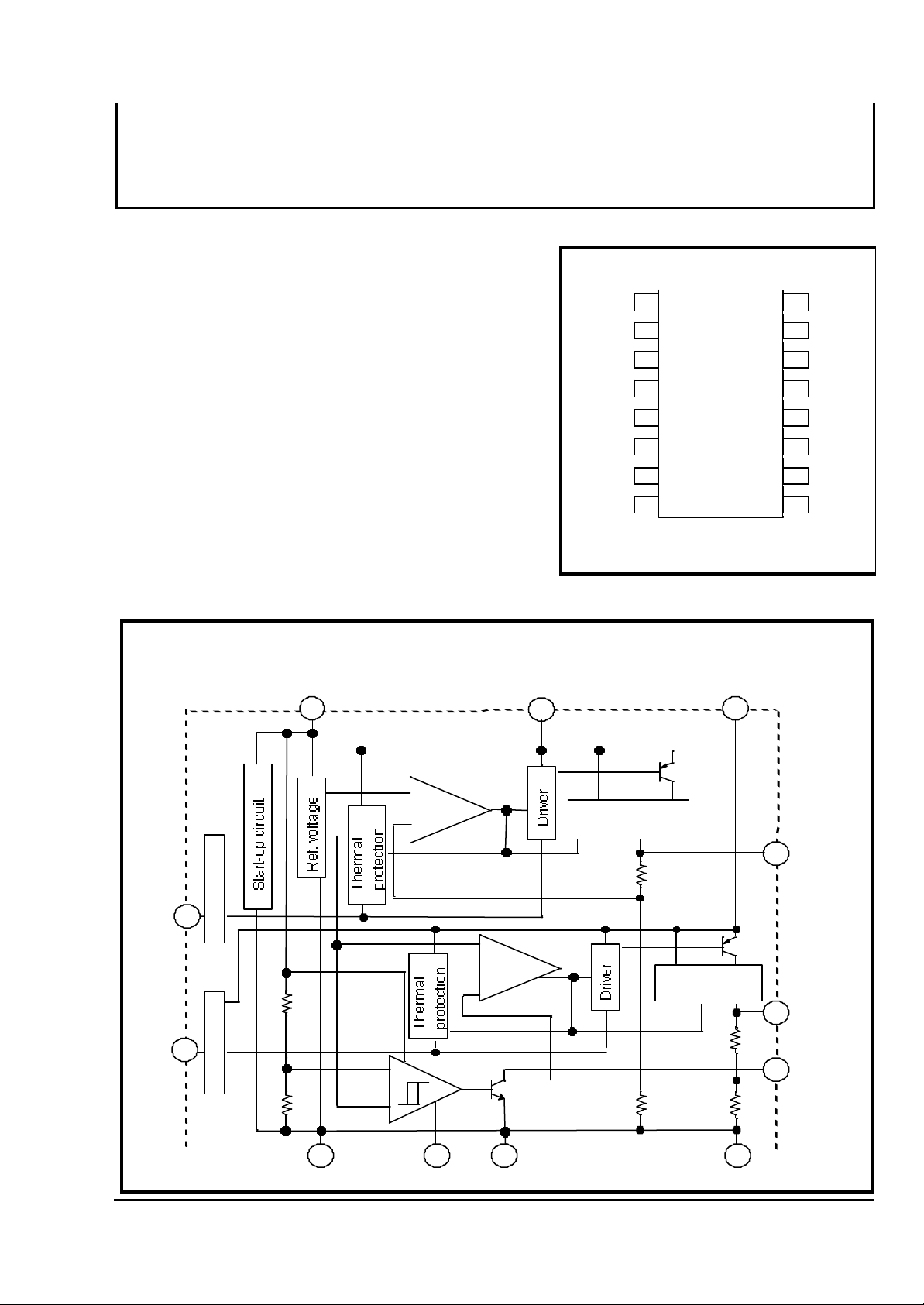
PIN CONFIGURATION(TOP VIEW)
1
VIN1
2
3
GND
4
VIN3
5
NC
6
7
8
VIN2 NC
Outline 16P2N-A
16
15
14
13
12
11
10
9
NC
NC
GND
Cd
GND
CH1
ON/OF
F
CH2
ON/OF
F
Note:Same voltage should be applied to VIN1,VIN2,and VIN3.
GND terminals(4pin, 11pin, 14pin) should be put together
VIN3
5
O
N
/
O
F
2
F
O
N
/
O
7
F
F
to be connected to GND.
+
Err.
Amp.
-
+
Err.
Amp.
VIN1
1
-
-
Overcurrent limit
circuit
Overcurrent limit
circuit
VIN2
8
15
10
3
Output1
Output2
Reset
output
GND
+
4
12 11
Cd
( /4)
1
13
GND
GND
000530
Page 2
MITSUBISHI<Standard LinearICs>
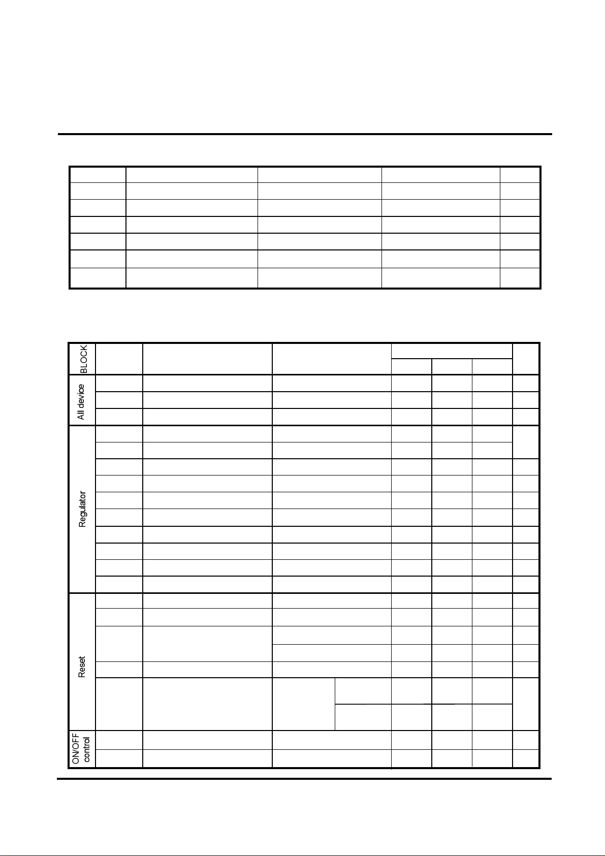
mWºCºC
300VmAmAV
VmVdB
mV
mAVmVµsV
V
100
200
80
20
10
0.3
IL=150mA
3.3
3.234
3.366
40
120
30
90
RL=2.2kΩ
RL=100kΩ
0.7
0.8
2.55
Cd=0µF
VOUT1+0.3
8
-0.3
0.4VV
V
µA
mV
20
ABSOLUTE MAXIMUM RATINGS(Ta=25ºC,unless otherwise noted.)
ELECTRICAL CHARACTERISTICS(Ta=25ºC, VIN=5V, CI=10µF, Co1=Co2=47µF, unless otherwise noed.)
PRELIMINARY
Symbol
VIN
IL
Pd
Kθ
Topr
Tstg
Symbol Parameter
VIN
Icc1
Icc2
VOUT1
VOUT2
VIO
Reg-IN
Reg-L1
Reg-L2
VNO
RR
IOS
TCVO
Vs
∆Vs
Parameter
Input voltage
Load current *1
Power dissipation
Thermal derating ratio
Operating temperature
Storage temperature
Supply voltage range
Circuit current
Circuit current at OFF
Output voltage(1ch)
Output voltage(2ch)
Input/output differential
Input regulation
Load regulation(1ch)
Load regulation(2ch)
Output noise voltage
Ripple rejection ratio
Output short holding current
Output voltage temp.coefficient
Detection voltage
Hysterisis voltage
M62525FP
HIGH PRECISION LOW INPUT/OUTPUT DIFFERENTIAL( 3.3V, 2.5V)
FIXED OUTPUT VOLTAGE REGULATOR WITH RESET
Condition Ratings Unit
-0.3~9
790
Max.
mW/ºCTa>25ºC
Unit
µVrms
mV/ºC
6.32
-20~+75
-40~+150
Test conditions
IL=0mA 2.2
VIN=4.4V~5.5V,IL=30mA
IL1=0mA~250mA
IL2=0mA~250mA
BW=10Hz~100KHz
vin=0dBm,f=120Hz,IL=30mA
Ta=-20~75∫C, IL=30mA
60
Limits
Typ.Min.
500VON/OFF1,VON/OFF2=0V
2.52.45
50
0.2
4.03.92 4.08
150
tpd
Vsat
VOPL
VON
VOFF
Delay time
Output saturation voltage
Threshold operating voltage
ON threshold voltage
OFF threshold voltage
VIN=3.5V, Isink=1mA 0.2 0.4
L reset type
minimum supply
voltage for IC
operation
( /4)
2
Vsat<0.4V
=
Vsat<0.4V
=
1.6 VIN+0.3
0.6
ms23Cd=0.1µF
0.7
000530
Page 3

MITSUBISHI<Standard LinearICs>
V
V
1
V
2
ON/OFF
PRELIMINARY
TIMING CHART
5V
Vs
IN
0V
5V
RESET
M62525FP
HIGH PRECISION LOW INPUT/OUTPUT DIFFERENTIAL( 3.3V, 2.5V)
FIXED OUTPUT VOLTAGE REGULATOR WITH RESET
∆Vs
tpd
OUT
OUT
1CH
ON/OFF
0V
3.3V
0V
2.5V
0V
H
L
2CH
H
L
( /4)
3
000530
Page 4

MITSUBISHI<Standard LinearICs>
PRELIMINARY
STANDARD CONNECTIONS
R
RESET
VIN
CI
+
ON/OFF1
M62525FP
HIGH PRECISION LOW INPUT/OUTPUT DIFFERENTIAL( 3.3V, 2.5V)
FIXED OUTPUT VOLTAGE REGULATOR WITH RESET
ON/OFF2
1
5
8
3
2
7
4
M62525FP
11 13
12
15
10
+
Cd
Co1
+
Co2
Vout1
IL1
Vout2
IL2
Note1. R is a pull-up resistance for reset terminal. 2.2kohm is recommended for the value.
Note2. C1 works for stabilizing input voltage. Recommended value is 10uF.
Note3. Co works for preventing the output voltage from oscillation. Minimum value is 10uF.
Recommended value is 47uF.
Note4. Delay time for reset is changeable by the capacitance connected to Cd terminal.
Even when no capacitor is connected, 30usec.(typ.) delay time is available.
Below shows how to set the delay time.
Delay time:Tpd(ms)=0.23×Cd(µF)
Example:when 0.1uF is connected to Cd terminal.
Tpd(ms)=0.23×0.1(µF)
=23(ms)
Note5. Connect ON/OFF terminal and VIN when ON/OFF function is not needed.
Note6. Get the capacitors close to IC terminals in case the operation is not stabilized by the
wiring resistance between each capacitor and IC terminals.
( /4)
4
000530
 Loading...