

Page 1
MITSUBISHI <Digi./Ana.INTERFACE>
PRELIMINALY
PRELIMINALY
Notices;This is not a final specification.
Some parametric limits are subject to change.
PWM IC for the synchronized deflection system control
GENERAL DESCRIPTION
The M62501P/FP is a controller for a deflection system of
CRT display monitors. It performs a stable PWM control over
a wide fluctuation of external signals, thanks to the built-in
trigger mode oscillator. The IC is suitable for an application to
a high voltage drive of monitors because of its following
circuits and functions;
• low voltage mulfunction protection circuit,
• over or under voltage protection circuit for a control line,
• soft-start function.
It is also applicable to a horizontal output correction.
FEATURES
• PWM output synchronized with external signals
• Wide pulse width modulation control frquency
15kHz to 150kHz
• Soft start function
• The under voltage output malfunction protection circuit
start Vcc > 9V stop Vcc < 6V
• Built-in over voltage protection (OVP) and under voltage
protection (UVP) control
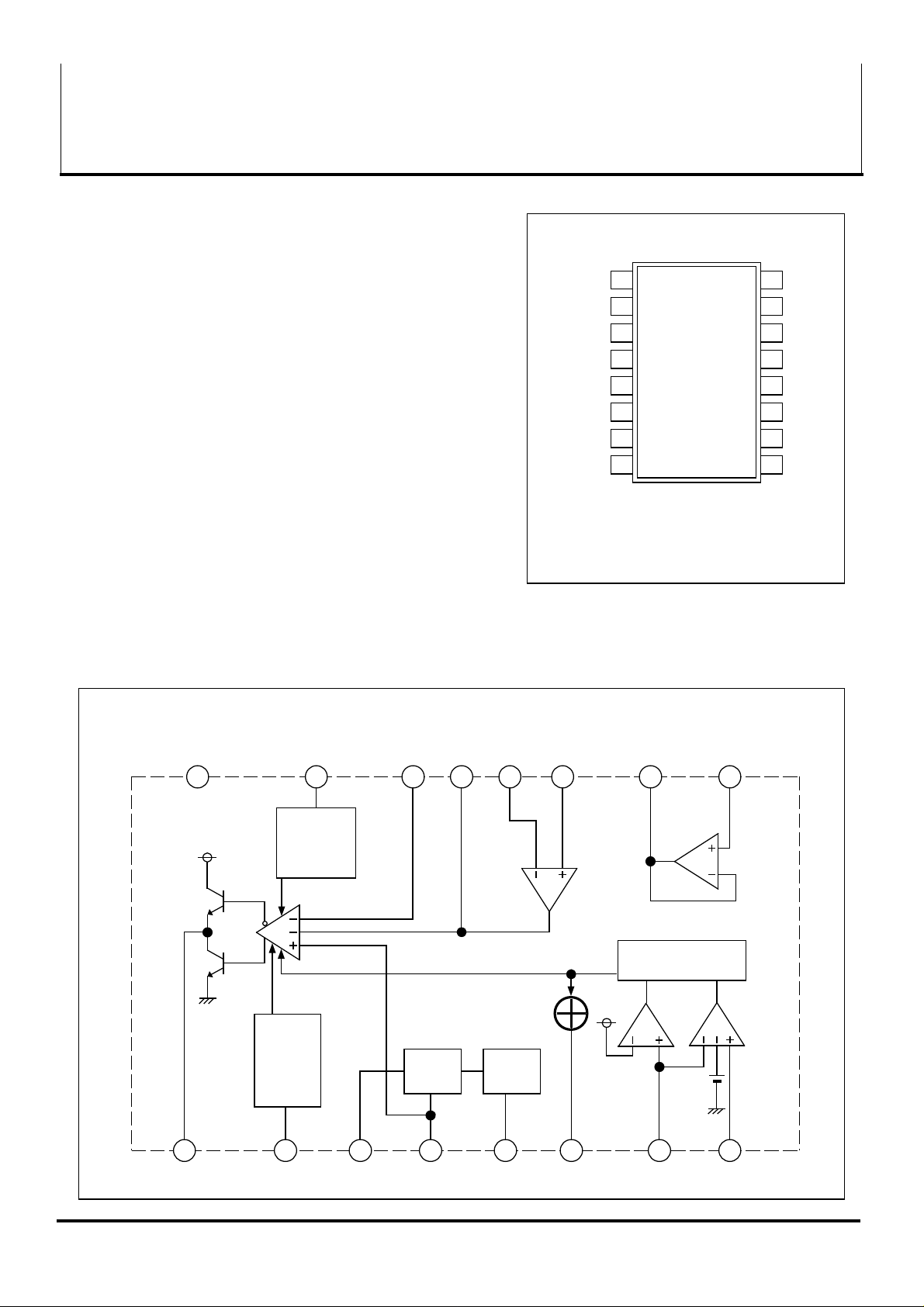
M62501P,FP
PIN CONFIGURATION(TOP VIEW)
Vcc
TIN
Cosc
Cagc
OVP
UVP
outline
1 16
2
3
4
5
6
7
8
M62501
15
14
13
12
11
10
P: 16P4
FP: 16P2S
PWM OUT
POUT
9
GND
VREF
DTC
FB
ININ+
BO
BI
APPLICATION
• CRT display monitor
BLOCK DIAGRAM
GND
16 15
VCC
VREF
VREF
Comp
UVLO
DTC FB IN- IN+ BO
14 13 12 11 10 9
Amp
Amp
Latch
VREF
CompComp
GEN
AGC
0.5V
PWM OUTBIVCC
( / 9 )
1
87654321
POUTCAGCTIN COSC
OVP UVP
9702
Page 2
MITSUBISHI <Digi./Ana.INTERFACE>
PRELIMINALY
PRELIMINALY
Notices;This is not a final specification.
Some parametric limits are subject to change.
Terminal Number and The facility
PIN No. Symbol Functional Description
PWM OUT PWM output1
VCC Power supply2
TIN Trigger input3
COSC Setting oscillating frequency4
CAGC AGC setting5
P.OUT Error signal output6
OVP Input of over voltage protection7
UVP Input of under voltage protection8
BI Positive input of buffer Amp.9
BO Output of buffer Amp.10
M62501P,FP
PWM IC for the synchronized deflection system control
IN+ Positive input of Op-Amp.11
IN- Negative input of Op-Amp.12
FB Output of Op-Amp.13
DTC Dead time control (Soft start function)14
VREF Output of reference voltage (5V)15
GND Ground16
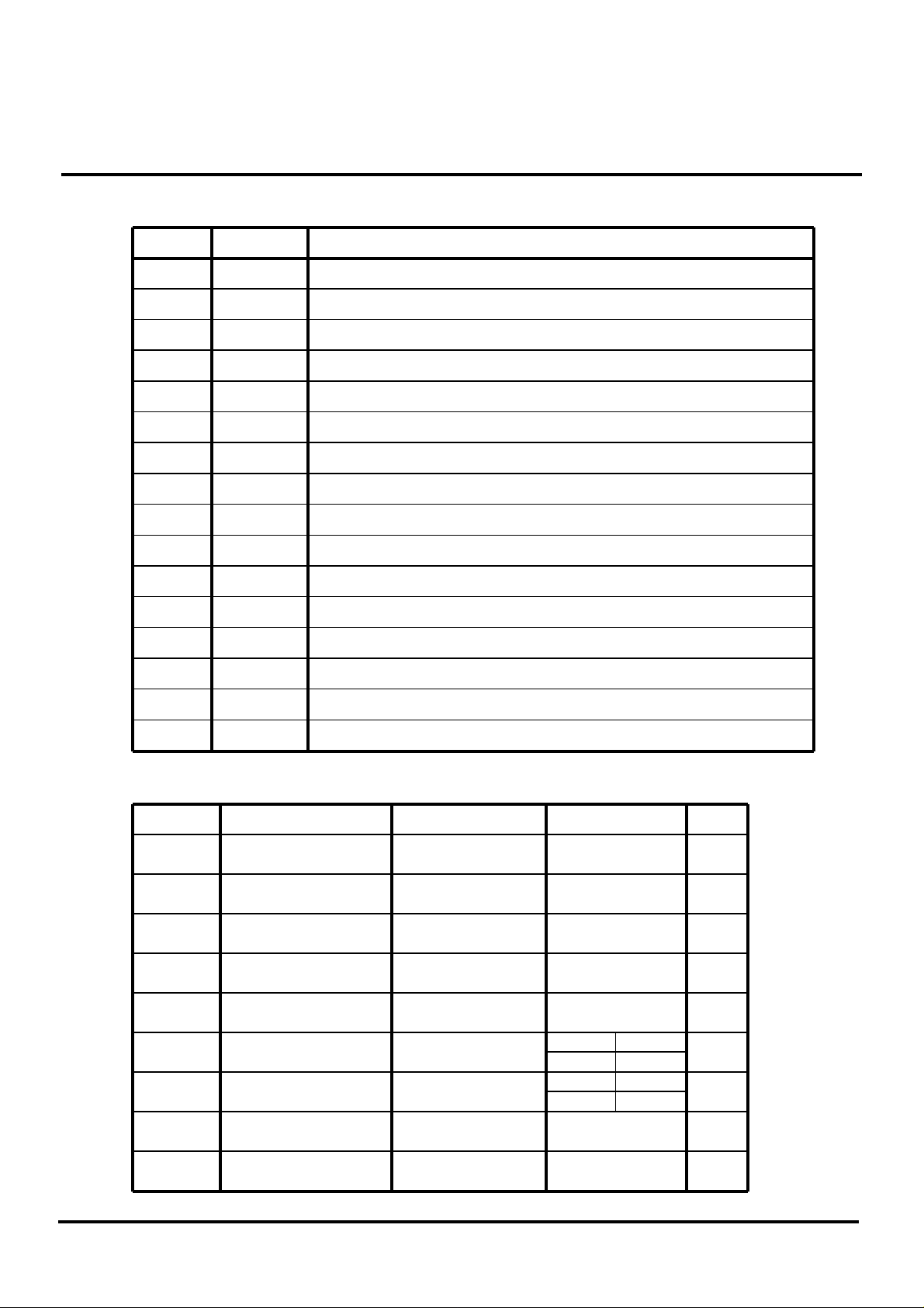
ABSOLUTE MAXIMUM RATINGS (Ta=25°C,unless otherwise noted)
Parameter Conditions Ratings UnitSymbol
VCC
VOUT
IOUT
VICM
VID
Pd
Kø
Topr
Supply voltage
Output voltage
Output current
Error Amplifier input
common mode voltage
Error Amplifier
differential input voltage
Power dissipation
Thermal derating
Operrating temperature
Ta ≥ 25°C
15
15
±100
-0.3 ~ VCC
VCC
P
1200 650
P
-20 ~ +75
FP
FP
5.29.6
mA
mW
mW/°C
°C
V
V
V
V
Tstg
Storage Temperature
( / 9 )
2
-40 ~ +150
°C
9702
Page 3
MITSUBISHI <Digi./Ana.INTERFACE>
PRELIMINALY
PRELIMINALY
Notices;This is not a final specification.
Some parametric limits are subject to change.
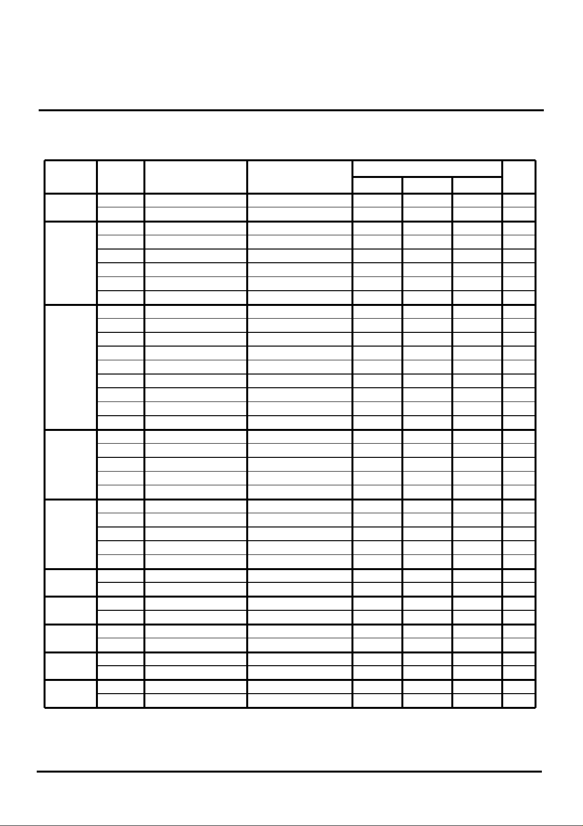
ELECTRICAL CHARACTERISTICS (Vcc = 12V, TIN = 40kHz, Ta = 25°C, unless otherwise noted)
Block
Symbol Parameter Test conditions
PWM IC for the synchronized deflection system control
M62501P,FP
Limits
Min Typ Max
All
Device
Reference
voltage
section
Error
Amp.
Buffer
Amp.
Oscillator
PWM
output
section
UVLO
section
OVP
section
UVP
section
P.OUT
section
VCC
ICC
VREF
Reg-in
Reg-L
TCVREF
IREF MAX
IS
VIO
IIb
IIO
VICM
AV
SR
VOR
Isink
Isourse
Ib
SR
VOR
Isink
Isource
fOSC
VOSC H
VOSC L
VTIN H
VTIN L
Vsat L
Vsat H
VTH ON
VTH OFF
VTH OVP
IIN OVP
VUVPO
IIN UVP
Vsat
IL
Range of power supply
Circuit current Output off mode
Reference voltage
Input regulation
Load regulation
Reference voltage thermal coefficient
Maximum reference current
Short-circuit current
Input offset voltage
Input bias current
Input offset current
Common mode input voltage range
Open loop transmission gain
Slew rate
Output voltage range
Output sink current
Output source current
Input bias current
Slew rate
Output voltage
Output sink current
Output source current
Oscillation frequency
The oscillator waveform bound voltage
The oscillator waveform lower limit voltage
High level of TIN
Low level of TIN
Output saturation voltage L
Output saturation voltage H
ON threshold voltage
OFF threshold voltage
OVP terminal threshold voltage
OVP terminal input current
Input offset voltage
UVP terminal input current
Output saturation voltage
Output leakage current
IREF=-5mA
Vcc=7 ~ 14V IREF=-5mA
IREF=0 ~ -5mA
IO=100mA
IO=-100mA
VPO=12V 1.0
VCC OFF 14
20
4.80
-100
-100
-0.3
70 110
0.3
10
-20
0.3 Vcc-2.5
2
15 150
2.5
9.5 10.5
8.0 10.0
4.75
5.00
1.0 10
2.0 20
0.01
-30
-30
4
4
3.5
1.5
0.7
9.0
6.0
5.00 5.25
5.20
100
VCC-2
VREF-1.5
-10
-10
VCC
1.0
1.4
6.65.4
1.0
1.0
0.4
Unit
V
mA
V
mV
mV
% / °C
mA
mA
7
7
mV
nA
nA
V
dB
V / µs
V
mA
mA
nA
V / µs
V
mA
mA
kHz
V
V
V
V
V
V
V
V
V
µA
mV
µA
VIPO=10mA
µA
( / 9 )
3
9702
Page 4

MITSUBISHI <Digi./Ana.INTERFACE>
PRELIMINALY
PRELIMINALY
Notices;This is not a final specification.
Some parametric limits are subject to change.
PWM IC for the synchronized deflection system control
Terminal functional description and equivalent circuit
Terminal No.
1 PWM OUT
2
3
Symbol Function and terminal circumscription circuitry
•PWM output terminal
•The PWM output synchronized with the TIN input.
•Output "H" level = 10.5V typ
(The output load current:-100mA,Vcc=12V)
•Output "L" level = 0.7V Typ
(The output load current:+100mA,Vcc=12V)
Vcc
Power supply terminal
Vcc
2 15
•Trigger input terminal
•Frequency range
15kHz ~ 150kHz
•It takes in a start edge.
TIN
3
TIN
TIN input waveform
MIN 2.5V
MAX 1.0V
M62501P,FP
Vcc
2
~
PWM
1
OUT
~
GND
16
VREF
~
4 Cosc
5
Cagc
16
•Cosc terminal
•It generates a saw wave by connecting capacitor between 4pin and GND.
•Recommended capacitor value is 1000pF.
•Cagc terminal
•It sets up sensitivity of AGC by connecting capacitor between 5pin and GND.
•Recommended capacitor value is 1µF.
VREF
15
Cosc
4
~
~
GND
~
16
5
GND
Cagc
( / 9 )
4
9702
Page 5

MITSUBISHI <Digi./Ana.INTERFACE>
PRELIMINALY
PRELIMINALY
Notices;This is not a final specification.
Some parametric limits are subject to change.
Terminal No.
Symbol Function and terminal circumscription circuitry
•The abnormal state detection output terminal
•The output becomes "H" from "L" when an abnormality is
detected in the OVP or UVP terminal. Then the PWM
output terminal becomes "H" settlement, too.
•Do OFF of power supply (Vcc) to remove latch of
6 POUT
abnormal state.
•In abnormal state detection ;
Output "H" level = 10.5V typ
(The output load current : no-load, Vcc=12V)
Output "L" level = 1.5V typ
(The output load current : -1mA, Vcc=12V)
•In normal state ;
Output "L" level = 0.4V typ
(The output load current : +10mA, Vcc=12V)
•Over voltage protection of the control line (OVP)
•Setting terminal voltage ;
GND ≤ VOVP < VREF
•Under voltage protection of the control line (UVP)
•Setting terminal voltage ;
GND ≤ VUVP < VOVP
M62501P,FP
PWM IC for the synchronized deflection system control
Vcc
2
~
POUT
6
~
GND
16
7 OVP
8 UVP
9
BI
2
Vcc
UVP
VREF
15
16GND
OVP
7
To latch input
8
Note:It is connected to GND when the abnormal detection terminal is not used.
•The input terminal of a buffer Amp. (BI)
•The output terminal of a buffer Amp. (BO)
Vcc
2
~
10
BO
( / 9 )
5
BI
9
~ ~
BO
10
~~
9702
Page 6

MITSUBISHI <Digi./Ana.INTERFACE>
PRELIMINALY
PRELIMINALY
Notices;This is not a final specification.
Some parametric limits are subject to change.
Terminal No.
Symbol
•Positive input terminal of an Op-Amp. (IN+)
•Negative input terminal of an Op-Amp. (IN-)
11 IN+
12 IN-
•Output terminal of an Op-Amp. (FB)
•Dead time control terminal (DTC)
•It can do soft start during power-on under keeping time constant.
13
FB
14 DTC
M62501P,FP
PWM IC for the synchronized deflection system control
Function and terminal circumscription circuitry
Vcc
2
DTC
FB
14
13
IN+
11
~ ~
~~
~~~
Cosc
4
15
12
IN-
VREF
~ ~
15 VREF
16 GND
PWM comparator section
•Reference voltage terminal
•5V output voltage
(The terminal can begin to take outside
connected load 5mA.)
•Ground terminal
Vcc
GND
GND
16
2
VREF
15
-
+
16
( / 9 )
6
9702
Page 7

MITSUBISHI <Digi./Ana.INTERFACE>
PRELIMINALY
PRELIMINALY
Notices;This is not a final specification.
Some parametric limits are subject to change.
M62501 APPLICATION
VCC
Vcc
PWM IC for the synchronized deflection system control
IN- IN+
R2 R3
D1
C3
R1
C5
C4
AGCGEN
VR1
C2
1516 914 13 12 11 10
VREF
UVLO
21 83 4 5 6 7
M62501P,FP
R4
Latch
VREF
Cosc Cagc
PWM OUT
C1,C2 Stabilization capacitors of Vcc and VREF.
VR1 It is decided considering a load capacity of VREF.
(A load capacity is approximately 5mA.)
Recommended value is around 10kΩ.
C3,D1 They are for the soft start function. A time constant is decided considering VR1.
Cagc This capacitor is for stabilization of AGC. A larger capacitor improves a stability of the
system, however a system response is degraded.
Recommended value is around 1µF.
Cosc This capacitor is for a saw wave generation. Recommended value is around 1000pF.
R1,R2,R3,R4 They are for a gain setting of the error Amp. R2 should be several kΩ to dozens of kΩ
C4,C5 to set a voltage gain 20dB to 40 dB at f = 1kHz, so that the feed back loop is stable.
When the voltage gain is too low, it causes jitter.
Recommended values of C4, C5 and R1 are ;
C4 = dozens of pF to several hundreds pF
C5 = several thousands pF to tens of thousands pF
R1 = dozens of kΩ to several hundreds kΩ.
*Annotation:Connect 7pin and 8pin terminal to GND when don't use under voltage protection (UVP).
TIN
C1
POUT
OVP UVP
( / 9 )
7
9702
Page 8

MITSUBISHI <Digi./Ana.INTERFACE>
PRELIMINALY
PRELIMINALY
Notices;This is not a final specification.
Some parametric limits are subject to change.
PWM IC for the synchronized deflection system control
EXAMPLE OF APPLICATION CIRCUIT
VCC
VREF
M62501P,FP
IN-
1516 914 13 12 11 10
Vcc
VREF
UVLO
21 83 4 5 6 7
Cosc Cagc
Tin
AGCGEN
POUT
Latch
( / 9 )
8
9702
Page 9

MITSUBISHI <Digi./Ana.INTERFACE>
PRELIMINALY
PRELIMINALY
Notices;This is not a final specification.
Some parametric limits are subject to change.
Timing chart
TIN
DTC
FB
PWM
OUT
•PWM OUT ON Duty is fixed in the voltage of higher one between
DTC terminal and FB terminal voltage.
M62501P,FP
PWM IC for the synchronized deflection system control
•Waveform at "H" was taken from "L", and having put TIN up
(PWM output is fixed in "H", too when fix TIN terminal in"H".)
TIN
PWM OUT
Approximately 150µsec
•Waveform at "L" was taken from "H",and having put TIN up
(PWM output is fixed in "L",too when fix TIN terminal in"L".)
TIN
PWM OUT
( / 9 )
9
9702
 Loading...