

Page 1

MITSUBISHI (Dig./Ana. INTERFACE)
(SWITCH)
M62500P/FP
SYNCHRONIZATION DEFLECTION SYSTEM CONTROL PWM IC
DESCRIPTION
The M62500 is a semiconductor integrated circuit designed and
developed as a deflection control of the CRT display monitor.
The built-in trigger mode oscillator allows stable PWM control to be
gained against a wide range of change of external signals.
The M62500 provides a low supply voltage output malfunction
preventive circuit (UVLO) and software start function optimum to
horizontal output correction of monitor, high voltage drive and high
voltage regulator.
FEATURES
PWM output in synchronization with external signals
Wide range of PWM control frequency
15kHz to 150kHz
The PWM output phase is adjustable against external signals
Soft start
Built-in low voltage output malfunction prevention circuit
Start VCC>9V
Stop VCC<6V
APPLICATION
CRT display monitor
PIN CONFIGURATION (TOP VIEW)
GND
VREF
Tin
Delay Adj
CAGC1
DTC
IN1 (+)
IN1 (-)
FB1
COLLECTOR1
OUT1
P.GND
1
2
3
4
Outline 24P4D (P)
24
VCC
23
DRIVE OUTPUT
22
Phase Adj
21
Duty Adj
DOUBLE SPEED
205
SWITCH
196
RAGC
187
CAGC2
178
IN2 (+)
169
IN2 (-)
1510
FB2
1411
COLLECTOR2
1312
OUT2
24P2V-A (FP)
BLOCK DIAGRAM
VCC RAGC CAGC2 IN2 (+) IN2 (-) FB2 COLLECTOR2 OUT2
WIND
COMP
VREF
1 2 3 4 5 6 7 8 9 11 12
GND
DRIVE
OUTPUT
VREF Tin Delay
Phase
Adj
PHASE
CONT
DUTY
CONT
GEN
DELAY
Duty
Adj
Adj
DOUBLE
SPEED
SWITCH
2021222324 13141516171819
EDGE
DETECTION
comp
AGC
CAGC1 DTC IN1 (+) IN1 (-) FB1 COLLECTOR1 OUT1 P. GND
GEN
AGC
OUTPUT START
START (VCC>9V)
STOP (VCC<6V)
VCC
10
( / 11 )
1
Page 2

SYNCHRONIZATION DEFLECTION SYSTEM CONTROL PWM IC
ABSOLUTE MAXIMUM RATINGS (Ta=25˚C, unless otherwise noted)
Symbol Ratings UnitParameter
VCC
VOUT
IOUT
Vd
Id
VICM
VID
Pd
K
Topr
Tstg
Note. For the polarity of current, the direction in which current flows to the IC is specified positive (+),
while the direction in which current flows out from the IC is specified to be negative (-).
Supply voltage
Output voltage
Output current
Drive output voltage
Drive output current
Common mode input voltage range of
error amplifier
Common mode differential input voltage
of error amplifier
Power dissipation
Thermal derating
Operating temperature
Storage temperature
15
15
±150
15
20
-0.3 to VCC V
VCC V
P
1400
P
11.2
-20 to +75 °C
-40 to +125 °C
FP
1000
FP
8
mA
mA
mW
mW/°C
MITSUBISHI (Dig./Ana. INTERFACE)
M62500P/FP
V
V
V
2
( / 11 )
Page 3
MITSUBISHI (Dig./Ana. INTERFACE)
M62500P/FP
SYNCHRONIZATION DEFLECTION SYSTEM CONTROL PWM IC
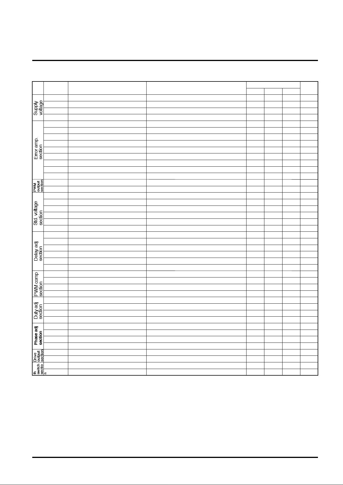
ELECTRICAL CHARACTERISTICS (VCC=12V, fIN=40kHz, Ta=25˚C, unless otherwise noted)
Block
Symbol Test conditions UnitParameter
VCC
ICC Without signal mA
VCC ON
VCC OFF
VIO
IIb
IIO
VICM
AV
SR
VOR V
Isink
Isource
VsatL IO=100mA
VsatH
VREF V
Reg-in
Reg-L
TCVREF
IREF MAX
IS
IIN
VIN L
VIN H
IDelay
TD min
TD max
IDTC
Vth U
Vth L
TDuty PWM output duty
IDuty
Duty min Minimum duty
Duty max Maximum duty
Duty
IPhase Input current
T2 min
T2 max
T2 Leading time of drive output
Vsat D Output saturation voltage
ILD
Ifh fh pin current
Vfh fh switching voltage
Note 1. Output must not be reversed with input of 0.
Range of power supply voltage
Dissipation current
Activation start voltage
Activation stop voltage
Input offset voltage
Input bias voltage
Input offset current
Common mode input range
Open loop gain
Through rate
Output voltage range 1)
Output sink current
Output source current
Output saturation voltage L
Output saturation voltage H
Reference voltage
Temperature coefficient of reference voltage
Short-circuit current
Input current
"L" input voltage
"H" input voltage
Input current
Minimum delay time
Maximum delay time
Input current
Upper limit voltage of saw tooth wave
Lower limit voltage of saw tooth wave
Input current
Duty
Minimum leading time of drive output
Minimum leading time of drive output
Output leak current
IO=-100mA
IREF=-5mA
VCC=7 to 14V IREF=-5mA
IREF=0 to -5mA
Ta=-20 to +75°C
VIN=5V
VDelay adj=0V
VDelay adj=3.0V
0.65VREF
0.28VREF
VDTC=2.5V
VDuty adj=2.5V
VDuty adj=2.5V
VPhase adj=2.5V
VPhase adj=1.0V
Id=10mA
VDO=12V
Vfh=5V
Limits
Min. Typ. Max.
20 40 70
8 9 10
-100 100
-0.3 VCC-2
0.3 VREF-1.5
0.7 1.4
4.80 5.00
-40
-70
— 200
-0.6 —
—
—
-6.5 -1.3
— 10
-3.5 -0.7
140
—
0.8
10
45 50
80 95
45
15
0.5
0.7VREF
0.3VREF
50
-10
5.20
—
1
—
0.75VREF
0.32VREF
55
—
20
—
55
—
7.0
430
VVCC off 14
V
V5.4 6.0 6.6
mV7
nA-100
nA
V
dB70 110
V/µs4
mA10
mA
V
V9.5 10.5
mV1 10Input stability
mV2 20Load voltage
%/°C0.01
mAMaximum reference current
mA
µA
V— 0.6
V2.0 —
µA-0.1
µs
µs
µA2.0
V
V
%
µA
%
%
%
µA
µs— 0.7 1.6
µs9 9.4 —
µs4.5 5.5
V0.4
µA1
µA— 330
V0.6VREF0.5VREF0.4VREF
( / 11 )
3
Page 4

EXPLANATION OF TERMINALS
Pin No. Function and peripheral circuit of pinsSymbol
1
GNDGND
MITSUBISHI (Dig./Ana. INTERFACE)
M62500P/FP
SYNCHRONIZATION DEFLECTION SYSTEM CONTROL PWM IC
VCC
2
3
VREF
Tin
5.0V reference voltage
External load of about 5mA can be taken out.
Trigger input
Read at the rising edge
Tin
2
VREF
S
Q
3
FF
R
VREF
Delay adjustment
4
5
18
Delay Adj
CAGC1
CAGC2
Delay of read trigger signal
VDelay : 0 to 3.0V
TDelay : 1µ to 10µsec
AGC capacitance
Connects capacitance between each pin
and GND and sets up AGC sensitivity
4
( / 11 )
4
VREF
5
18
Page 5

EXPLANATION OF TERMINALS (Cont.)
Pin No. Function and peripheral circuit of pinsSymbol
MITSUBISHI (Dig./Ana. INTERFACE)
M62500P/FP
SYNCHRONIZATION DEFLECTION SYSTEM CONTROL PWM IC
6
7
8
16
17
9
15
DTC
IN1 (+)
IN1 (-)
IN2 (-)
IN2 (+)
FB1
FB2
Dead time control
(PWM comparator + pin)
Air amplifier input pin
Air amplifier output
(PWM comparator + input pin)
6
VCC
17
7
8
16
VCC
9
15
10
14
10
11
12
13
14
COLLECTOR1
OUT1
P.GND
OUT2
COLLECTOR2
PWM output section
11
12
VREF
13
AGC current setup
19
RAGC
Connects resistance between pin
19
and GND and sets up AGC current on the OUT2 side.
19
5
( / 11 )
Page 6

EXPLANATION OF TERMINALS (Cont.)
Pin No. Function and peripheral circuit of pinsSymbol
MITSUBISHI (Dig./Ana. INTERFACE)
M62500P/FP
SYNCHRONIZATION DEFLECTION SYSTEM CONTROL PWM IC
Double speed switch
VREF
Switches frequency of OUT2
20
fh/2fh
and drive output to the double frequency.
OPEN, GND fh
20
VREF 2fh
VREF
21
22
Phase Adj
Duty adjustment of drive output Duty Adj
Phase adjustment of drive output against OUT2 (T2)
DRIVE
OUT
OUT2
T2
21
VREF
22
VREF
23
24
VCC Supply terminal
Open collector outputDRIVE OUTPUT
6
( / 11 )
23
Page 7

APPLICATION EXAMPLE
MITSUBISHI (Dig./Ana. INTERFACE)
M62500P/FP
SYNCHRONIZATION DEFLECTION SYSTEM CONTROL PWM IC
VR2
D1 C4
VR1
1
2
3
4
R6
Tin
+IN1
-IN1
OUT1
Cagc1
R2
R4
R3
C1
R1
C2
C4 C3
R5
C1, C10 : Is required for stabilization of Vcc and VREF.
Is normally set to tens of µF to hundreds of
µF.
VR 1, 2, 3, 4 : Is determined taking into account the load
capability of VREF. (External load capability
of approx. 5mA) Shall be normally set to
approx. 10kΩ.
C2, C8, C9 : Is added to high impedance pin of voltage
control for improvement in noise margin.
Depends on the device installation
environment. Shall be normally set to approx.
0.1µF.
C4, D1 : Is added for the execution of software start.
Set a time constant, taking into account the
set value of VR2.
R1 : Is added to reduce interference by Tin and
outputs. With VIN=approx. 2.5V to 5V, the
resistance value of approx. 22kΩ is
recommended.
Cagc 1, 2 : Capacitance necessary for stabilization of
AGC. As the capacitance is larger, the
stability is larger, but the characteristic of
answering becomes worse. The capacitance
value of 1µF is recommended.
VCC
VR4
VR3
C6C5
Cagc2
R10
R8
R11
C10
DOUT
C9
C8
C7
Ragc
+IN2
-IN2
OUT2
R12
24
23
22
21
205
196
187
178
169
1510
1411
1312
R9
R7
R2, R3, R10, R11 : A gain setup constant of error Amp. To
R4, R5, R8, R9 assure the stability of feedback, R4 and R8
C3, C4, C5, C6 shall be set to several kΩ to tens of kΩ to set
the gain to approx. 20dB to 40dB with f=1
kHz. If the gain is too low, jitter may take
place. It is therefore recommended to set C3
and C5 to tens of pF to hundreds of pF, C4
and C6 to thousands of pF to tens of
thousands of pF, and R5 and R9 to tens of
kΩ to hundreds of kΩ.
Ragc : Resistance for setting AGC on the OUT2
side. Is set with Ragc=27kΩ.
C7 : If f to be input into Tin suddenly changes,
addition of C7 shortens non-control time of
Dout (output of "H"). As a capacitance value,
it is recommended to adopt 2.2µF. In the
case of adding C7, however,
Cagc2≥0.68µF is recommended.
R6, R7 : Current limit resistance of OUT1/2. Is
normally set to several Ω. Insertion of direct
limit resistance into OUT1/2 pin is also
effective.
R12 : Pull-up resistance of DOUT output. DOUT is
an open collector output and requires R12. Is
normally set to several kΩ.
* Note: To reduce interference in the signal system, pins GND and
12
P.GND shall be grounded at a point in the power supply block.
1
( / 11 )
7
Page 8

SYNCHRONIZATION DEFLECTION SYSTEM CONTROL PWM IC
SETUP OF VOLTAGE CONTROL BLOCK
TD vs. VDELAY Adj CHARACTERISTICS (f=40kHz)
20
MITSUBISHI (Dig./Ana. INTERFACE)
M62500P/FP
Applying a voltage to the DELAY Adj pin can control the delay time
of OUT1 to TIN.
10
0
0
2.0
VDELAY Adj (V)
PWM OUTPUT MINIMUM DUTY vs. VDTC
CHARACTERISTICS (f=40kHz)
100
80
60
40
20
0
0
2
VDTC (V)
4.0
TIN
TD TD
OUT1
Applying a voltage to the DTC pin can control the dead time of
PWM output.
TH
OUT1, 2
T
PWM output minimum duty
41 3
TDUTY= X100 (%)
TH
T
T2 vs. VPhase CHARACTERISTICS (f=40kHz)
10
8
6
4
2
0
1 2 3 5
0
4
VPhase (V)
Applying a voltage to the Phase Adj pin can control a leading time
of drive output to OUT2.
DRIVE OUT
8
( / 11 )
OUT2
T2
T2
Page 9

T2 vs. f CHARACTERISTICS
10
MITSUBISHI (Dig./Ana. INTERFACE)
M62500P/FP
SYNCHRONIZATION DEFLECTION SYSTEM CONTROL PWM IC
8
6
4
2
0
0
50
TIN f (kHz)
DRIVE OUTPUT DUTY vs. VDUTY
CHARACTERISTICS (f=40kHz)
100
80
60
40
VPhase=2300mV
VPhase=1350mV
VPhase=650mV
VPhase=250mV
100 150
Applying a voltage to the DUTY Adj pin can control drive output
duty.
TH
Drive output
T
20
0
0
2
41 3
Drive output duty
TDUTY= X100 (%)
TH
T
VDUTY (V)
9
( / 11 )
Page 10

ABCDF
E
TIME CHART
VCC
DRIVE
OUTPUT
PHASE
ADJ
PHASE
CONT
DUTY
ADJ
MITSUBISHI (Dig./Ana. INTERFACE)
M62500P/FP
SYNCHRONIZATION DEFLECTION SYSTEM CONTROL PWM IC
DOUBLE
SPEED
SWITCH
2021222324 13141516171819
RAGC CAGC2 IN2 (+) IN2 (-) FB2 COLLECTOR2 OUT2
PIN WAVE
EDGE
DUTY
WIND
COMP
VREF
1 2 3 4 5 6 7 8 9 11 12
GND
VREF Tin Delay
CONT
GEN
DELAY
DETECTION
(SWITCH)
comp
AGC
CAGC1 DTC IN1 (+) IN1 (-) FB1 COLLECTOR1 OUT1 P. GND
Adj
GEN
AGC
OUTPUT START
START (VCC>9V)
STOP (VCC<6V)
VCC
10
3
PIN
TIN
A POINT
B POINT
11
PIN
OUT1
D POINT
TD
10
( / 11 )
FB1
9
PIN
C POINT
Page 11

PIN WAVE (Cont.)
MITSUBISHI (Dig./Ana. INTERFACE)
M62500P/FP
SYNCHRONIZATION DEFLECTION SYSTEM CONTROL PWM IC
D POINT
E POINT
PIN
PIN
20
Low
20
High
F POINT
PIN
OUT2
PIN
D.OUT
E POINT
F POINT
PIN
OUT2
PIN
D.OUT
13
23
13
23
PWM OUT NON-CONTROL STATUS
FB2
15
PIN
T1
T2 TL TH
With trigger input at pin
Without trigger at pin (in case of GND)
3
FB>3.5V, FB>DTC
OUT1, 2
FB<1.5V, FB>DTC
3
OUT1, 2
High
( / 11 )
11
3.5V
1.5V
Low (GND)
 Loading...