

Page 1
MITSUBISHI SOUND PROCESSOR ICs
MITSUBISHI SOUND PROCESSOR ICs
M62475FP
AUTOMATICADJUSTMENTCDPREAMPLIFIER SERVOCONTROLLER
AUTOMATIC ADJUSTMENT CD PREAMPLIFIER SERVO CONTROLLER
M62475FP
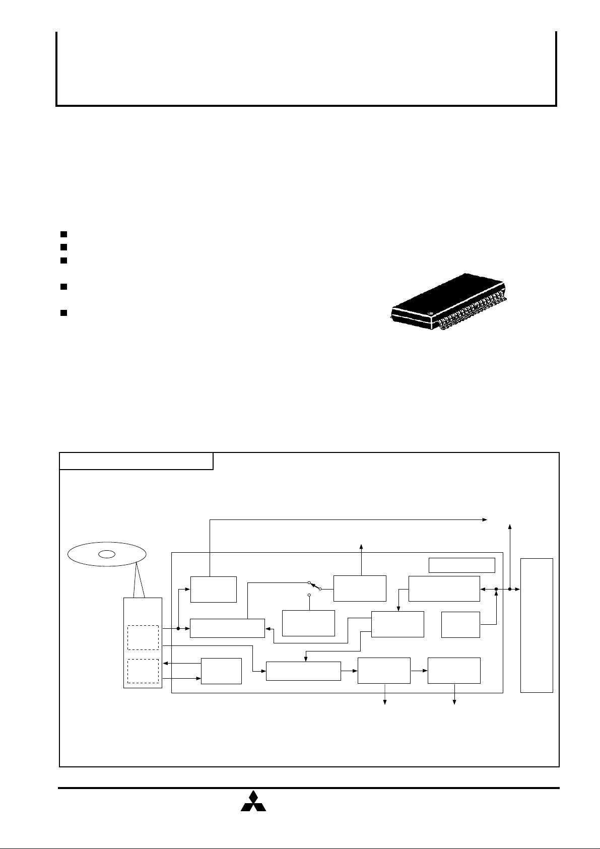
DESCRIPTION
The M62475FP is an IC that contains preamplifier/servo amplifier necessary for optical pickup servo
control for CD player.
This IC also supports automatic adjustment with microcomputer control.
FEATURES
Pickup servo control can consist of the M62475FP only
Supporting 3-beam system
Built-in serial data command interface with MCU to reduce load
on MCU
Built-in circuit for automatically adjusting tracking balance,
tracking/focus gain
Built-in internal self reset circuit
RECOMMENDED OPERATING CONDITIONS
Supply voltage range..............................................VCC=4.5 to 5.5V
Rated supply voltage.......................................................... VCC=5V
SYSTEM CONFIGURATION
HF
PREAMPLIFIER
OPTICAL
PICK-UP
PD
FE PREAMPLIFIER
FOCUS
SEARCH
FOCUS ACTUATOR
FOCUS
SERVO
AUTOMATIC
ADJUSTMENT
Outline 42P2R-A
0.8 mm pitch 450 mil SSOP
(8.4 mmX17.5 mmX2.0 mm)
M62475FP
MCU I/F
RESET
DSP for CD
MCU
for
CONTROL
LD
APC
TE PREAMPLIFIER
MITSUBISHI
ELECTRIC
TRACKING
SERVO
TRACKING
ACTUATOR
SLIDE SERVO
SLIDE
MOTOR
( / 19 )
1
Page 2
MITSUBISHI SOUND PROCESSOR ICs
M62475FP
AUTOMATIC ADJUSTMENT CD PREAMPLIFIER SERVO CONT ROLLER
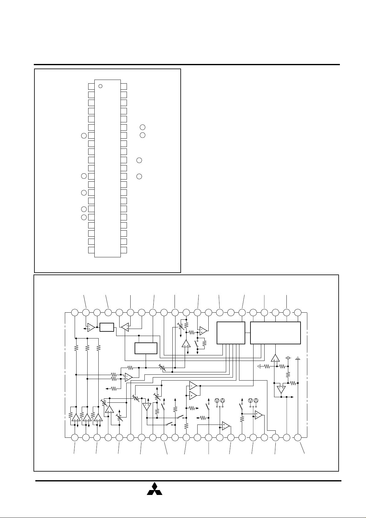
PIN CONFIGURATION (TOP VIEW)
A
SGT
TE
TEG
TG1SW
TE OUT
TC/SHOCK
TS
TG2SW
TS
TS OUT
SS
SS
SS OUT
DETFIL
BIAS
GND
1
2
B
C
3
E
4
5
F
6
7
8
9
10
11
+
12
13
-
14
15 28
+
16 27
-
17 26
18 25
19 24
20 23
21 22
Outline 42P2R-A
42
41
40
39
38
37
36
35
34
M62475FP
33
32
31
30
29
ABC
HFI
HFO
MRC
APC OUT
-
APC
+
APC
CFSR
SGF
FE
-
FEG
-
FS
FSOUT
CC
V
RIREF
CLPF
DOUT
MSD
MCK
JP1/SG
MLA/DIS
BUILT-IN FUNCTION
•IV amplifier
•HF amplifier:HF (High Frequency Amp.)
•Focus Error Amplifier:FE (Focus Error Amp.)
•Focus Servo Amplifier:FS (Focus Servo Amp.)
•Tracking Error Amplifier:TE (Tracking Error Amp.)
•Tracking Servo Amplifier:TS (Tracking Servo Amp.)
•Sledge Motor Servo Amplifier:SS (Sledge Servo Amp.)
•Switching Circuit for Jump Brake:
TG1SW, TG2SW (Tracking Gain SW)
JF SW, JR SW (Jump Forward/Reverse SW)
SF SW, SR SW (Sledge Forward/Reverse SW)
•Focus Search Circuit
Search Signal Generator
FSOK Detector
•Track Cross Detector: TC Det (Track Cross Detector)
•Shock Detector: SC Det (Shock Detector)
•Logic Controller:
Serial Data Command Interface
Jump, Brake, Focus Search Control
Adjustment Control
•Vcc/2 generation circuit
•Auto Laser Power Control: APC (Automatic laser Power Control)
•HF Bottom Level Detector
•MR Detector
•Automatic Adjustment Circuit
Tracking balance adjustment circuit
Tracking gain adjustment circuit
Focus gain adjustment circuit
Gain adjustment signal generation and phase detection circuit
IC INTERNAL BLOCK DIAGRAM
HF
REVERSE INPUT
ABC
OUTPUT
A+B+C
A
INPUT
CONSTANT
FOR MIRROR
HF
OUTPUT
HF
AMPLIFIER
10k 10k 4.7k
I/V
AMPLIFIER
18k39k39k
ABCEF
B
INPUT
C
INPUT
REVERSE INPUT
APC
OUTPUT
MR
MIRROR
220k
220k
220k
E
INPUT
F
INPUT
CONSTANT
FOR
APC
38 32
220k
5 11
SGT
OUTPUT
TE REVERSE
FOCUS
SEARCH
APC NONREVERSE
INPUT
36 34
35
APC
FOCUS
SEARCH
A-B
TE
AMPLIFIER
7 9
8
TE GAIN
CONTROLTEOUT
INPUT
REVERSE
SGF
OUTPUT
TG1
2.2k
TS1
TG1
SW
FE
INPUT
FE GAIN
CONTROLFSOUTPUT
334142
SW
TC/SH SW
100k
SW
1021
TC/
SHOCK
FS
REVERSE
INPUT
2.2k
22k
FS
SW
FE
AMPLIFIER
TC/SHOCK DET
TG2
47k
SW
47k
TS NON-
REVERSE
INPUT
POWER
SUPPLY
REFERENCE
CURRENT
30 29 27
FS
12k
SW
ADJUST
JRSWJF
TS
AMPLIFIER
AMPLIFIER
22k
13 14 16
TS
REVERSE
INPUT
TG2
SWTSOUTPUT
CONSTANT
FOR
ADJUSTMENT
FILTER
DATA
INPUT
DATA
OUTPUT
28 22
15 21
SS
SW
22k
SS NON-
REVERSE
INPUT
REVERSE
INPUT
26 24
25
47k
SRSWSF
SW
17 19
18
SS
OUTPUT
INPUT
SS
CONSTANT FOR
ADJUSTMENT
CLOCK
INPUT
I/F
RESET
56k
SS
AMPLIFIER
REFERENCE
VOLTAGE
FILTER
JP1
INPUT
233140 39 37
47k
(COM)
20123 4 6
LATCH
INPUT
47k
BIAS
VCC/2
GND
MITSUBISHI
ELECTRIC
( / 19 )
2
Page 3
AUTOMATIC ADJUSTMENT CD PREAMPLIFIER SERVO CONT ROLLER
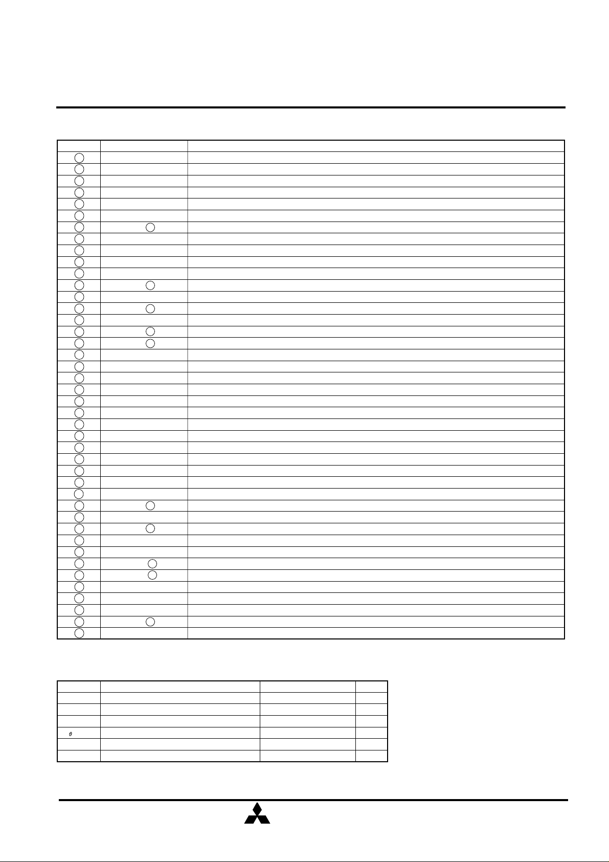
PIN DESCRIPTION
Pin No. Symbol Function
1
2
3
4
5
6
7
8
9
10
11
12
13
14
15
16
17
18
19
20
21
22
23
24
25
26
27
28
29
30
31
32
33
34
35
36
37
38
39
40
41
42
A
B
C
E
F
SGT
-
TE
TEG
TG1 SW
TE OUT
TC/SHOCK
+
TS
TG2 SW
-
TS
TS OUT
+
SS
-
SS
SS OUT
DET FIL
BIAS
GND
MLA/DIS
JP1/SG
MCK
MSD
DOUT
CLPF
IREF
Vcc
FSOUT
-
FS
FEG
-
FE
SGF
CFSR
+
APC
-
APC
APC OUT
MRC
HF OUT
-
HF
ABC
I-V amplifier A input
I-V amplifier B input
I-V amplifier C input
I-V amplifier E input
I-V amplifier F input
Tracking servo signal output
TE amplifier reverse input
TE amplifier gain control
Tracking gain select switch 1
TE amplifier output
Tracking cross/shock detector input
TS amplifier non-reverse input
Tracking gain select switch 2
TS amplifier reverse input
TS amplifier output
SS non-reverse input
SS amplifier reverse input
SS output
Detector filter for gain adjustment
Vcc/2 voltage output
Ground
Latch of serial data from microcomputer to servo IC/discharge of LPF for automatic adjustment
Control signal of 1 track jump brake pluse/Input of gain adjustment clock
Serial data transfer clock from microcomputer to servo IC
Microcomputer serial data
Output of data to microcomputer
Connects capacitor for determining the constant for automatic adjustment LPF
Connects resistance for setting current value of reference supply current
Power supply
FS amplifier output
FS amplifier reverse input
FE amplifier gain control
FE amplifier reverse input
Focus servo signal output
Connects the capacitor to determine the constant for focus search waveform
APC amplifier non-reverse input
APC amplifier reverse input
APC amplifier output
Constant for mirror
HF amplifier output
HF amplifier reverse input
IV amplifier (A+B+C) output
MITSUBISHI SOUND PROCESSOR ICs
M62475FP
ABSOLUTE MAXIMUM RATINGS (Ta=25˚C, unless otherwise noted)
Symbol Parameter Ratings Unit
VCC
VI
Pd
K
T
opr
Tstg
Supply voltage
Input voltage
Power dissipation
Thermal derating (Ta 25˚C)
Operating ambient temperature
Storage temperature
5
0 to V
CC
750
7.5
-20 to +75
-40 to +125
MITSUBISHI
ELECTRIC
V
V
mV
mW/˚C
˚C
˚C
3
( / 19 )
Page 4
MITSUBISHI SOUND PROCESSOR ICs
AUTOMATIC ADJUSTMENT CD PREAMPLIFIER SERVO CONT ROLLER
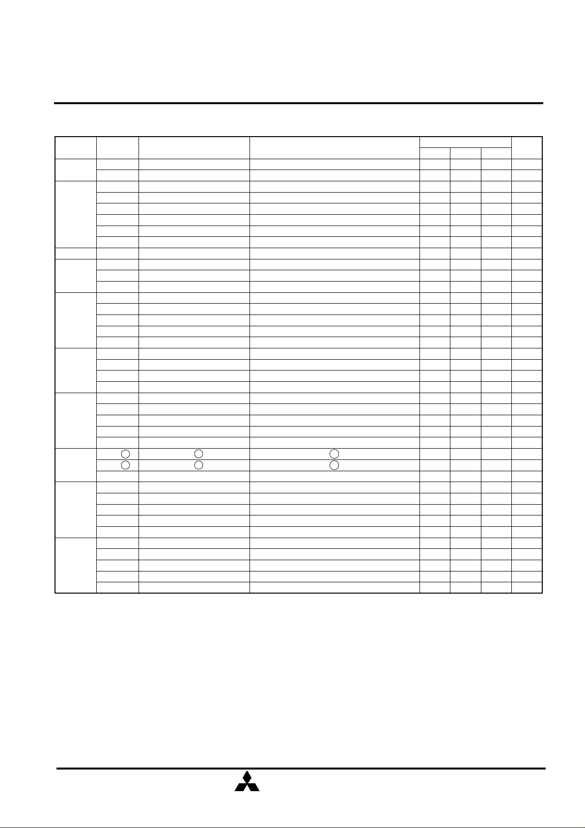
ELECTRICAL CHARACTERISTICS (Ta=25˚C, Vcc=5V, f=1kHz, CBA=100, unless otherwise noted)
M62475FP
Block
—
HF
FS OK
MR
APC
FE
FS
FSR
TE
TS
Symbol
Icc
V
REF
GVHFAB
GVHFC
fHF
VHHF
VLHF
VOSHF
VTFK
RMN
RMJ
fMR
GVAP
ATTAP
VHAP
VLAP
VOSAP
GVFE
VHFE
VLFE
BALFE
GVFS
ATTFS
VHFS
VLFS
VOSFS
VFSR
VFSR
VFZC
GVTE
VHTE
VLTE
VOSTE
BALTE
GVTS
ATTTS
VHTS
VLTS
VOSTS
Parameter
Circuit current
Reference voltage
Gain (input A/B)
Gain (input C)
Frequency characteristics
Output voltage "H"
Output voltage "L"
Output offset
FSOK level
Ratio (normal)
Ratio (jump)
Frequency characteristics
Gain
Attenuation (APC OFF)
Output voltage "H"
Output voltage "L"
Input offset
Gain
Output voltage "H"
Output voltage "L"
Balance
Gain
Attenuation (FS OFF)
Output voltage "H"
Output voltage "L"
Output offset
+
Focus search voltage
-
Focus search voltage
Focus zero cross voltage
Gain
Output voltage "H"
Output voltage "L"
Output offset
Track balance
Gain
Attenuation (TS OFF)
Output voltage "H"
Output voltage "L"
Output offset
Test conditions
With no signal provided, after reset
With no signal provided, after reset
f=500kHz,Vi=0.5V
f=500kHz,Vi=0.5VP-P
Vi=0.5VP-P
Vi=4.0V
Vi=1.0V
VREF reference
VREF reference
"Shock" mode
"Brake" mode
"Shock" mode
Vi=20mVrms
Comparison with GVAP
Vi=4.0V
Vi=1.0V
VREF reference
Vi=10mVrms
Vi=4.0V
Vi=1.0V
Comparison with G
Vi=50mVrms
Comparison with GVFS
Vi=4.0V
Vi=1.0V
VREF reference
+
-
VREF reference, pin
VREF reference, pin
VREF reference
Vi=50mVrms
Vi=4.0V
Vi=1.0V
VREF reference
VREF reference
Vi=50mVrms
Comparison with G
Vi=4.0V
Vi=1.0V
VREF reference
P-P
VFE
35
35
VTS
Limits
Min. Typ.
20.0 30.0
2.4 2.5
3.1 5.1
9.7 11.7
1.4 2.0
3.5 4.0
—
-60 0
-0.22 -0.16
0.35 0.45
0.46 0.56
4.0
-10 0
3.5 4.0
—
19.3 21.3
3.5 4.0
—
-50 0
+0.6 +0.8
-1.0 -0.8
-0.22 -0.16
7.0 9.0
3.5 4.0
—
-25 0
-1.5 +1.5
-0.6 1.4
3.5 4.0
—
-25 0
1.0
20 30
25 27
—
60
—
——
24
1.0
-2 0
——
60
1.0
1.0
——
60
1.0
Max.
-0.10
-0.10
40.0
2.6
7.1
13.7
—
—
1.5
+60
0.55
0.66
—
29
—
—
1.0
+10
6
—
1.5
+2
23.3
—
1.5
+50
+1.0
-0.6
11.0
—
1.5
+25
+4.5
3.4
—
1.5
+25
Unit
mA
V
dB
dB
MHz
V
V
mV
V
—
—
kHz
dB
dB
V
V
mV
dB
V
V
%
dB
dB
V
V
mV
V
V
V
dB
V
V
mV
%
dB
dB
V
V
mV
MITSUBISHI
ELECTRIC
( / 19 )
4
Page 5
MITSUBISHI SOUND PROCESSOR ICs
AUTOMATIC ADJUSTMENT CD PREAMPLIFIER SERVO CONT ROLLER
ELECTRICAL CHARACTERISTICS (Ta=25˚C, Vcc=5V, f=1kHz, CBA=100, unless otherwise noted) (cont.)
M62475FP
—
TC
SHOCK
TG
SS
RESET
ADJ
CMP
SG
Symbol
VJF
VJR
+
TC
V
-
VTC
+
VSH
-
VSH
ATG1ON
ATG1OFF
ATG2ON
ATG2OFF
GVTS
ATTSS
VHSS
VLSS
VOSSS
VSF
VSR
VRST
VORST
GVFE(max)
GVFE(min)
GVTE(max)
GVTE(min)
BALTE(max)
BALTE(min)
+
VPhFE
VPhFE
+
VPhTE
VPhTE
+
VBAL
-
VBAL
GLADJ
+
Vthc
-
Vthc
GLC
+
VSGF
-
VSGF
+
VSGT
-
VSGT
ParameterBlock
Jump voltage (forward)
Jump voltage (reverse)
Track cross voltage
Track cross voltage
Shock voltage mV
Shock voltage
+
-
+
-
Attenuation (TG1 ON)
Attenuation (TG1 OFF)
Attenuation (TG2 ON)
Attenuation (TG2 OFF)
Gain
Attenuation (SS OFF)
Output voltage "H"
Output voltage "L"
Output offset voltage
Slide voltage (forward)
Slide voltage (reverse)
Reset voltage
Output voltage
Max. gain (FE)
Min. gain (FE)
Max. gain (TE)
"JF" mode, VREF reference
"JR" mode, VREF reference
"Brake" mode, VREF reference
"Brake" mode, VREF reference
"Shock" mode, VREF reference
"Shock" mode, VREF reference
"Shock" mode, VREF reference
"Shock" mode, VREF reference
"Shock" mode, VREF reference
"Shock" mode, VREF reference
Vi=50mVrms
Comparison with G
Vi=4.0V
Vi=1.0V
VREF reference
"SF" mode, VREF reference
"SR" mode, VREF reference
20
Pin
36
Pin , after RESET
Focus gain" mode CBA=111
"Focus gain" mode CBA=000
"Track gain" mode CBA=111
Test conditions
+0.10 +0.15 +0.20
+42.5 +62.5 +82.5
VSS
+0.65 +0.95 +1.25
Limits
Min. Typ. Max.
-0.20 -0.15 -0.10
-42.5 -62.5
+110 +140 +170
-170 -140 -110
10 20
—
02
10 20
—
02
10 12 14
—
60
3.5 4.0
—
1.0 1.5
-25 0
-1.25 -0.95
-0.65
2.1 2.3 2.5
3.5 4.5
3.5 5.5 7.5
-3.5 -1.5
19 21 23 dB
"Track gain" mode CBA=000
Max. balance (TE)
Min. balance (TE)
Phase difference voltage
-
Phase difference voltage
Phase difference voltage
-
Phase difference voltage
Balance voltage
Balance voltage
Phase detection exit low pass filter gain
+
-
Comparator level
Comparator level
Low pass filter gain
+
SGF output voltage
-
SGF output voltage
+
SGT output voltage
-
SGT output voltage
"Track balance" mode CBA=111
"Track balance" mode CBA=000
+
-
+
-
"Focus gain" mode phase difference (90+30)˚
"Focus gain" mode phase difference (90-30)˚
"Track gain" mode phase difference (90+30)˚
"Track gain" mode phase difference (90-30)˚
"Track balance" mode +0.5V offset
"Track balance" mode -0.5V offset
19
C (Pin )=680pF
+
-
VREF reference
VREF reference
27
C (Pin )=2.2nF
34
Pin , VREF reference
34
Pin , VREF reference
6
Pin , VREF reference
6
Pin , VREF reference
8.0 11.0 14.0 %
-12.8 -9.8 -6.8
3.1 3.3 3.5 V
-5 -3
—
—
-5 -3
0.6 0.7 0.8 V
-0.8 -0.7 -0.6 V
0.6
0.7
-0.8 -0.7 -0.6
82.5
—
—
—
—
+25
—
0.5 dB
3.5
1.9
-1 dB
-1
0.8
Unit
V
V
mV
mV
mV
dB
dB
dB
dB
dB
dB
V
V
mV
V
V
V
V
dB
dBMin. gain (TE) 12 1614
%
V3.1 3.3
V1.5 1.7
V1.5 1.7 1.9
V2.8 3.0 3.2
V1.8 2.0 2.2
mV0 +50
mV-50 0
dB
V
V
MITSUBISHI
ELECTRIC
( / 19 )
5
Page 6
MITSUBISHI SOUND PROCESSOR ICs
/
M62475FP
AUTOMATIC ADJUSTMENT CD PREAMPLIFIER SERVO CONT ROLLER
FUNCTION DESCRIPTION
SettingBuilt-in Constant Current Source Current Value
The current value of Tracking Servo (TS) and Sledge Servo (SS)
constant current can be set with resistance value Rx connected
between pin and Vcc.
If the absolute values for TS and SS constant source current
values are assumed to be I (JF, JR) and I (SF, SR), respectively, they
are set as follows.
I (JF. JR) =
I (SF, SR) =
Where, V is the voltage of pin . If the voltage of pin (GND)
is assumed to be V , V can be found by the following formula.
V = V + VBE (VBE = 0.7V standard)
28
1
8
1
4
28
28 21
CURRENT
REFERENCE
28
CC-V
V
•
Rx
28
CC-V
V
•
Rx
2821
VCC
RX
28 29 14
V
BE
28
17
21
M62475FP
EQUIVALENT CIRCUIT
B
M62475FP
ZERO CROSS
A
35 31 30
FOCUS SEARCH
CIRCUIT
DETECTION
FZC OPE RATION TIMING CHARTCONSTANT CURRENT SOURCE BLOCK D IAGR AM
FOCUS SEARCH
OPERATION
tup
A
B
Vref
FSR+
V
Vref
VFSR-
VA
VB
SEARCH
VOLTAGE
tFSR
FOCUS SERVO ON
tdown
t
t
Vc
IJF I JR
FSR Detector
When the focus search is performed, the focus search direction is
automatically switched.
The focus search always starts from the side. The polarity (
-
direction) internal logic signal of the focus search voltage is
used for control and switching.
FZC detection is effective only in a direction.
+
ISF ISR
Setting FSR time tFSR (CFSR setting)
C
FSR
tFSR=
IFSR
+
CFSR:CFSR pin external capacitor
35
IFSR:Focus search current
At time of rising:110µA
At time of falling:60µA
FSR Vth± Voltage setting
Vth+:Vref+0.7V
Vth-:Vref-0.7V
MITSUBISHI
ELECTRIC
( / 19 )
6
Page 7

MITSUBISHI SOUND PROCESSOR ICs
j
r
j
M62475FP
AUTOMATIC ADJUSTMENT CD PREAMPLIFIER SERVO CONT ROLLER
AUTOMATIC ADJUSTMENT FUNCTION
The IC is capable of automatically adjusting the three places of
tracking balance, tracking gain and focus gain.
TRACKING BALANCE ADJUSTMENT
The input resistance of the I/V conversion amplifier connected to E
and F pickups and the 8-step adjustment resistance built in a
feedback resistance are switched for the adjustment. The
adjustment precision is approximately 3% by the step.
The automatic adjustment operation enters an oscillation signal
from the automatic adjustment signal generator of MCU into a
servo loop to forcibly make the beam cross the track. When this is
the case, the output voltage of I/V conversion amplifier is
integrated. If the E and F output signals are well balanced and are
the same, an error voltage is not generated in the output voltage
after this integration and a reference voltage is obtained. If they
are not balanced, a voltage of a DC component is generated. The
result of having compared this output voltage and the reference
voltage is converted into a logical level and is then output to the
monitor terminal. The MCU is used for control and the result is
udged. According to the result, the adjustment resistance of the
I/V conversion amplifier is sequentially switched step by step fo
the adjustment in the direction of reversing the current logical
result. At the time when the result has been reversed, the error is
udged to be put within a one-step error and the adjustment is
complete.
TRACKING FOCUS GAIN ADJ USTMENT
The input resistance of the tracking focus error amplifier and the 8step adjustment resistance built in a feedback resistance are
switched for the adjustment. The adjustment precision is
approximately 1 dB by the step.
The adjustment operation enters an oscillation signal with the
output gain of -3 dB in a servo loop from the automatic adjustment
signal generator of MCU into a servo loop to forcibly generate a
gap in the track and focus. A waveform adjusted signal of the
generated tracking focus error signal and the MCU oscillation
signal are collated with each other with respect to the phase and is
then integrated to convert the phase difference into the voltage.
The result of having compared this output voltage and the
reference voltage is converted into a logical level and is then
output to the monitor terminal. The MCU is used for control and
the result is judged. According to the result, the input resistance of
the amplifier is sequentially switched step by step in feedback
resistance for the adjustment in the direction of reversing the
current logical result. At the time when the result has been
reversed, the error is judged to be put within a one-step error and
the adjustment is complete.
EQUIVALENT CIRCUIT (Tracking Balance)
PD
FE
ADJUSTMENT
BIAS
VOLTAGE
ADJUSTMENT
RESISTANCE
VOLTAGE
COMPARATOR
I/V CONVERSION
AMPLIFIER
RESISTANCE
BIAS
VOLTAGE
EQUIVALENT CIRCUIT (Tracking Focus Gain)
GAIN ADJUSTMENT
ERROR AMPLIFIER
TRACKING ACTUATOR
OR FOCUS ACTUATOR
VOLTAGE
COMPARISON
EX-OR
MCU
COMMAND
LATCH SIGNAL
BIAS
VOLTAGE
ACTUATOR
TRACKING
ACTUATOR
MONITOR
TERMINAL
(to MCU)
To DATA-OUT
MCU
MITSUBISHI
ELECTRIC
( / 19 )
7
Page 8

AUTOMATIC ADJUSTMENT CD PREAMPLIFIER SERVO CONT ROLLER
AUTOMATIC ADJUSTMENT FLOWCHART
BASIC ROUTINE
Serial data command: XXOOOCBA (XX is specified according to
the adjustment command.)
START
Initialization for XX
MITSUBISHI SOUND PROCESSOR ICs
AUTOMATIC ADJUSTMENT EXAMPLE
V
Vthc+
CLPF PIN
27
Vref
Vthc-
M62475FP
t
DATA OUT=0
YES
CBA > 0
YES
Setting of CBA CBA-1
DATA OUT=1
YES
Setting of CBA CBA+1
END
NO
NO
NO NO
CBA < 7
YES
Setting of CBA CBA+1
DATA OUT=0
YES
Setting of CBA CBA-1
NO
DOUT PIN
MCU CHECK
ADJ COMMAND
END OF
ADJUSTMENT
CLPF PIN
27
DOUT PIN
MCU CHECK
ADJ COMMAND
END OF
ADJUSTMENT
POINT
Vthc+
Vref
Vthc-
POINT
26
0
765CBA=4
V
26
0
565CBA=4
t
6
t
t
MITSUBISHI
ELECTRIC
( / 19 )
8
Page 9

MITSUBISHI SOUND PROCESSOR ICs
M62475FP
AUTOMATIC ADJUSTMENT CD PREAMPLIFIER SERVO CONT ROLLER
SERIAL COMMAND FUNCTION
An 8-bit shift register is installed in the logic controller to convert
(decode) serial data (MSD pin ) from the microcomputer into a
command for the servo IC.
25
FUNCTION DESCRIPTION of Data-IN
Of the 8-bit data, high order 4 bits (D7 to D4) is used to select a
command mode and low-order 4 bits (D3 to D0) are used to set
(instruct) the command status.
Commands in the same mode can be given concurrently with data
transferred once. They are held until new data is entered.
Therefore, the command status is held if another mode is selected.
SERIAL COMMAND FUNCTION TABLE
MSD pin input
Command Name
D7 D6 D5 D4 D3 D2 D1 D0
SERVO 0 0 SledgeTrackFocus FSOK/TC
Track balance 0 1 ADJABC
Track Gain 01 ADJABC
Focus Gain 11 ADJABC
Note 1. Output from DOUT pins is automatically switched by selecting each mode.
2. The status in the Servo Mode is set with two bits for each of command Track (D3,D2) and sledge(D1,D0).
25
Mode selection Command status setting
Brake
/Shock
———
25
———
———
Data out
pin output
COMMAND FUNCTION TABLE
Command Function
Brake
Shock
Track
Sledge
Mode Data
D5FocusFS ON
Track1
Track2
D4
D3 D2
00
01
10
11
D3 D2
00
01
10
11
1 ON
0 OFF
1
0
TS OFF
JR
JF
TS ON
SS OFF
SR
SF
SS ON
• APC amplifier ON
• Focus search start to servo ON (PS SW="OPEN")
• APC amplifier OFF
• Focus servo OFF (FS SW = "CLOSE")
Jump brake (jump setting) operation
Opens/closes TSSW.
Controls SW 'TG SW' for track gain switching.
Track servo OFF
Reverse jump
Forward jump
Track servo ON
Sledge servo OFF
Reverse sledge
Forward sledge
Sledge servo ON
For TSSW, JF SW, and JR SW, refer to 'TRACK
Function Table'.
For SS SW, SF SW, and SR SW, refer to 'TRACK
Function Table'.
MITSUBISHI
ELECTRIC
( / 19 )
9
Page 10

AUTOMATIC ADJUSTMENT CD PREAMPLIFIER SERVO CONT ROLLER
k
k
j
SERIAL DATA (MSD) TRANSFER METHOD
Data is transferred with LSB first and the MLA signal is sent to
execute the command.
SERIAL DATA INPUT TIMING CHART
MSD
25
PIN INPUT
MCK
24
PIN INPUT
MLA
22
PIN INPUT
LOGIC INPUT CONDITIONS
Symbol
fck
twck
tsu
th
t
d
twl
Clock frequency
Clock pulse width
Setup time
Hold time
Delay time
Latch pulse width
LSB MSB
twc
twck
1/fck
tsu
th
Test conditions
MITSUBISHI SOUND PROCESSOR ICs
M62475FP
D6D5D4D3D2D1D0 D7
td twl
Limits
Min. Typ. Max.
—
100 200
2.5 5
0.1 0.2
2.5 5
2.5 5
15
—
—
—
—
—
UnitParameter
kHz
µs
µs
µs
µs
µs
BRAKE
Setting the break command to "1" performs the jump brake
operation to improve the jump setting capability after the trac
ump.
Jump Brake Operation
The track servo loop is set to OFF with TC=" " (at the falling
edge of TCDet output) when MR is 1.
The track servo loop is set to ON with TC=" " (at the falling
edge of TCDet) when MR is 0.
Jump Brake True Value List (Effective in the TS ON mode)
INPUT
MIRROR
TC Det TS SW status
1 ("Mirror")
0 ("Track")
Note 3. TC/SHSW "CLOSE", TG SW "OPEN"
OUTPUT
OPEN (track servo OFF)
CLOSE (track servo ON)
"1"
"0"
TRACK CROSS DET
VREF-62.5mV VREF+62.5mV
TE
SHOCK
With the SHOCK command set to "1", the shock operation is
carried out to switch the track gain at time of shock.
Jump Brake Operation
With SHOCK detect=1, the track gain is placed in the shock
mode.
With SHOCK Det=0, the track gain is placed in the normal
mode.
Shock True Value List (Effective in the TS ON mode)
OUTPUTINPUT
SHOCK Det
1 ("SHOCK")
Note4. TC/SH SW "OPEN"
0 ("NORMAL")
+-
5. V and V are set with external constant.
TG SW status
OPEN (Shock mode)
CLOSE (Normal mode)
"1"
"0"
SHOCK DETECTOR
-
V
VREF
TE
+
V
MITSUBISHI
( / 19 )
10
ELECTRIC
Page 11

TRACK FUNCTION TABLE
j
INPUT
COMMAND
TS OFF
JR
JF
TS ON
DATA
D3 D2 TS SW
00
001
1
11
OPEN (Servo OFF)
OPEN (Servo OFF)
OPEN (Servo OFF)
CLOSE (Servo ON)
SLEDGE FUNCTION LIST
INPUT
COMMAND
SS OFF
SR
SF
SS ON
DATA
D1 D0
00
001
1
11
CLOSE (Sledge OFF)
CLOSE (Sledge OFF)
CLOSE (Sledge OFF)
OPEN (Sledge ON)
AUTOMATIC ADJUSTMENT CD PREAMPLIFIER SERVO CONT ROLLER
OUTPUT (SW Status)
OUTPUT (SW status)
TS SW
JF SW
OFF
OFF
ON
OFF
SF SW
OFF
OFF
ON
OFF
MITSUBISHI SOUND PROCESSOR ICs
M62475FP
JR SW
OFF
ON
OFF
OFF
JR SW
OFF
ON
OFF
OFF
DIRECT COMMAND FUNCTION
JP1 signal
When a 1-track jump takes place, serial data to be transferred
twice can be omitted to control the amount of delay in processing
time.
JP1 is generally set to "1". When JP1 is set to "0" with TC (Data
out) signal set to "1", the logic controller automatically reverses the
ump polarity (JF to JR or JR to JF).
When a jump is complete (after fixed time Ta), switching JP1 from
"0" to "1" can automatically terminate JF and JR to select the TR
ON/SSON status.
Signal Waveform with a jump
KICK PULSE (JF OR JR)
TS OUT
JP1
Ta
BRAKE PULSE
MITSUBISHI
( / 19 )
11
ELECTRIC
Page 12

JP1 SIGNAL TRUE VALUE LIST
MITSUBISHI SOUND PROCESSOR ICs
M62475FP
AUTOMATIC ADJUSTMENT CD PREAMPLIFIER SERVO CONT ROLLER
1 0
0 1
JP1
(INPUT)
1
00 11 10 01 00 11 10 01
TSOFF TS ON JF JR SS OFF SS ON SF SR
TSOFF TS ON JR JF SS OFF SS ON SR SF
TSOFF TS ON JF
TRACK (D3, D2) SLEDGE (D3, D2)
LOGIC OUTPUT FUNCTION
Data out
Data out output is switched according to the serial command (D6,
D7="0", "0") mode (see the serial command function list).
The output corresponding to the serial command mode sent last is
given.
Data Out Output Corresponding List
Data out signal name
(1)
(2)
(1) FS ON
With FS SW=OPEN (servo ON), FSOK "0" is output.
FSOK
TC
Serial command mode (input)
FOCUS (0010XXXX)
TRACK (0001XXXX)
FSOK TRUE VALUE LIST
Input
FF SW status
CLOSE (Servo OFF)
CLOSE (Servo ON)
While FS OK is set to "1", TS SW is open (servo OFF) and SS SW
is open regardless of the command status.
Output
FSOK
1
0
TRACK mode
JR
(2) TC
The TC signal that latches the MR signal at the edge (falling edge)
of TCDet output is output.
SS OFF SS ON SF
SR
TC TRUE VALUE LIST
MR
"1"Mirror
"0"Track
Input
TC Det
Output
TC
1
0
MR signal detector
Detects an envelope of the HF signal and sends data to the
internal logic controller.
MITSUBISHI
ELECTRIC
( / 19 )
12
Page 13

AUTOMATIC ADJUSTMENT CD PREAMPLIFIER SERVO CONT ROLLER
CONTROL METHOD FLOWCHART EXAMPLE
Note:Since this description applies to an example on the item
related to the servo, take into account the entire system when
using this. In addition, pay attention to the
simplification/reduction of actions in abnormal status.
1
POWER_RESET :Processing with power turned on
2
DISC_START :Disk start processing
3
BALANCE_ADJ :Track balance processing
4
TRACK_ADJ :Track gain adjustment
5
FOCUS_ADJ :Focus gain adjustment
6
ADJUST :Adjustment routine
7
SE_OUT :Adjustment signal output routine
8
Jump control
8-1. SINGLE_JUMP
8-2. SHORT_JUMP
8-3. MID_JUMP
8-4. LONG_JUMP
1
POWER_RESET
POWER_RESET
System initialization
MITSUBISHI SOUND PROCESSOR ICs
2
DISC_START
DISC_START
Pick-up innermost
circumference ?
YES
Move pick-up to outside
[00000010] sending
Spindle motor rotation start
Wait 50
msec
FOCUS ON sending
[00100000]
Data Out=0 ?
YES
Track servo ON
[00101111] sending
NO
NO
M62475FP
Move inside
[00000001] sending
FOCUS servo
check
Set adjustment initial value
(Send the default value)
BAL=100
FOC=100
TRA=100
END
Note:BAL :Track balance
FOC:Focus gain
TRA :Track gain
FOCUS_ADJ
BALANCE_ADJ
HFD=0
CRC=1 ?
YES
TRACK_ADJ
FOCUS_ADJ
BALANCE_ADJ
END
Note:Pick-up servo operation preparatory completion. For example,
reading TOC requires to move pick-up to the innermost circumference.
Focus gain preparatory adjustment
Track balance conflict adjustment
NO
Tracking gain adjustment
Focus gain adjustment
Track balance adjustment
DSP read check
MITSUBISHI
ELECTRIC
( / 19 )
13
Page 14

MITSUBISHI SOUND PROCESSOR ICs
M62475FP
AUTOMATIC ADJUSTMENT CD PREAMPLIFIER SERVO CONT ROLLER
3
BALANCE_ADJ TRACK_ADJ FOCUS_ADJ
BALANCE_ADJ
HFD=1
ZZ=01
CBA=BAL
ADJUST
BAL=CBA
HFD=0
END
ADJUST SG_OUT
6 7
ADJUST
T=50
SG_OUT
T=25
4
TRACK_ADJ
CBA=TRA
TRA=CBA
ZZ=10
ADJUST
END
SG_OUT
Send [ZZ000CBA]
No latch signal
Hold "L" for T msec latch signal
5
FOCUS_ADJ
ZZ=11
CBA=FOC
ADJUST
FOC=CBA
END
(For T msec LPF capacitor discharge)
Data Out=0 ?
YES
CBA > 0 ?
YES
CBA=CBA-1
SG_OUT
Data Out=1
YES
CBA=CBA+1
Send [ZZ000CBA]
END
NO
NO
NO
CBA < 7 ?
YES
CBA=CBA+1
SG_OUT
Data Out=0
YES
CBA=CBA-1
NO
NO
ZZ=11
YES
JP1
1300 Hz output
for 160 msec
END
Note: Set the frequency of the adjustment signal according to the system.
NO
ZZ=10
YES
JP1
1800 Hz output
for 160 msec
NO
JP1
80 Hz output
for 160 msec
MITSUBISHI
ELECTRIC
( / 19 )
14
Page 15

MITSUBISHI SOUND PROCESSOR ICs
M62475FP
AUTOMATIC ADJUSTMENT CD PREAMPLIFIER SERVO CONT ROLLER
Jump control
8
The jump control is divided into the following four types according to
(Note) Put the check routing of the HFD status in a program. Read the main
routine and sub-codes for check, regardless the jump control.
the track count.
Type
8-1. SINGLE_JUMP
8-2. SHORT_JUMP
8-3. MID_JUMP
8-4. LONG_JUMP
N: Track count (standard)
1 to 5
6 to 16
to 100
to 1000
Data Out=0
YES
HFD=0
8-1. SINGLE_JUMP 8-2. SHORT_JUMP
SINGLE_JUMP
Move to the inside
YES
Send [00100100] Send [00101000]
Send [00111111]
(No latch signal)
NO
Move to the outside
NO
HFD=1
SHORT_JUMP
HFD=1
Send [00100100] Send [00101000]
COUNT
HFD=1
DATA OUT=1
YES
JP1=0
Wait 260µsec
Send latch signal
Wait 5µsec
N=N-1
N=0
YES
Send [00111111]
JP1=1
END
NO
NO
JP1=0
Set timer to 5 msec
SJ1
CATCH
JP1=1
SJ2
Wait 15msec
Send [00101111]
JP1=1
HFD=0
END
MITSUBISHI
ELECTRIC
( / 19 )
15
Page 16

MITSUBISHI SOUND PROCESSOR ICs
M62475FP
AUTOMATIC ADJUSTMENT CD PREAMPLIFIER SERVO CONT ROLLER
Set timer to 5 msec
NO
COUNT
NBY2=N/2
DATA OUT=1
YES
Time over
YES
NO
NO
NBY2=N/2
NBY2 > 0
YES
DATA OUT=1
YES
Time over
YES
END
NO
NO
CATCH
Send [00111111]
(No latch signal)
JP1=0
LC=180µsec/ (Loop time)
LOOPN=LC
DATA OUT=1
YES
NO
NO
Time over ?
YES
LC=LC-1
LC=0
NO
LC=LOOPN
DATA OUT=1
YES
Time over ?
YES
LC=LC-1
NO
NO
Send latch pulse
END
NO
LC=0
YES
MITSUBISHI
ELECTRIC
( / 19 )
16
Page 17

MITSUBISHI SOUND PROCESSOR ICs
AUTOMATIC ADJUSTMENT CD PREAMPLIFIER SERVO CONT ROLLER
8-3. MID_JUMP 8-4. LONG_JUMP
M62475FP
MID_JUMP
JP1=1
Move to the outside
YES
Send [00111010] Send [00110101]
Wait 4msec
HFD=1
JP1=0
Set timer to 8 msec
CATCH
SJ2
NO
(Jump to the
SHORT_JUMP label)
LONG_JUMP
Move to the outside
YES
Send [00111010] Send [00110101]
HFD=1
Wait 150msec
Send [00111000]
Wait 30msec
Set the timer to 120 msec
SJ2
NO
(Jump to the
SHORT_JUMP label)
MITSUBISHI
ELECTRIC
( / 19 )
17
Page 18

TEST CIRCUIT
0.047µ
10k
MITSUBISHI SOUND PROCESSOR ICs
M62475FP
AUTOMATIC ADJUSTMENT CD PREAMPLIFIER SERVO CONT ROLLER
5V
10µ
22µ
470k
2.2n
100n
MRC
E
1k1k
100k
22k
-
APC
APC OUT
F
SGT
47k 100k 1k 2.2k
+
APC
TE
100k4.7M
0.047µ
CFSR
TEG
200k1.8k 2.2k4.7k
100k1.2M 150k
-
SGF
FE
TG1SW
TE OUT
FEG
TC/
SHOCK
56k
FS
+
TS
1k 39k 4.7k
CC
V
FSOUT
TG2SWTSTS OUTSSSS
RIREF
-
6.8k 100k
100k
CLPF
+
6.8k1.8k
18k
1µ
18k
42 41 40 39 38 37 36 35 34 33 32 31 30 29 28 27 26 25 24 23 22
HFI
ABC
A
1 2 3 4 5 6 7 8 9 10 11 12 13 14 15 16 17 18 19 20 21
39k 39k 18k 220k 220k
HFO
B
C
CONTROLLER
MSD
DOUT
SS OUT
22k
2.2k
680p
TEST
MCK
DETFIL
JP1/SG
BIAS
47µ
MLA/DIS
GND
MITSUBISHI
ELECTRIC
Units Resistance :
Capacitance:F
( / 19 )
18
Page 19

TYPICAL CHARACTERISTICS
µ
µ
THERMALDERATING (MAXIMUM RATING)
1000
800
750
600
400
375
200
POWER DISSIPATION Pd (mW)
0
25 50 75 125
0
AMBIENT TEMPERATURE Ta (˚C)
MITSUBISHI SOUND PROCESSOR ICs
M62475FP
AUTOMATIC ADJUSTMENT CD PREAMPLIFIER SERVO CONT ROLLER
100
APPLICATION EXAMPLE
39p
6.8k
10k
6.8k
0.47µ
42 41 40 39 38 37 36 35 34 33 32 31 30 29 28 27 26 25 24 23 22
HF
A+B+C
10k 10k 4.7k
ABCEF
2 3 4 5 6 7 8 9 10 11 12 13 14 15 16 17 18 19 20 21
1
22k
27
47
10k
100n
APC
MIRROR
220k
220k
220k
220k
18k39k39k
SEARCH
A-B
1M
1k
10
FOCUS
TE
82k
100p
1.5M
5.6k
2.2k
TG1
SW
3.3M 100k
FE
100k
TS1
SW
56k
3.3k
0.22µ
15k
22n
1k39k
82p
2.2k
22k
FS
SW
47k
TC/SH SW
47k
1µ
22n
68k
22n
680k
TG2
SW
22k
F.ACT
FS
12k
100
100n
MLA
47µ
56k
2.2µ
ADJUST
JRSWJF
SW
SS
SW
22k
TS
6.8k
100k
0.22µ
39k
T.Act SL.Motor
HFD
SW
2.2µ
5.6k
DATA OUT
DATA IN
47k
SRSWSF
SS
39k
100n
10k
MCU
CLOCK
I/F
RESET
56k
47k
Units
MLA/DISCH
JP1/SG
47k
BIAS
(COM)
VCC/2
4.7µ
Resistance:
Capacitance:
CD DSP
F
MITSUBISHI
( / 19 )
19
ELECTRIC
 Loading...