

Page 1
MITSUBISHI SOUND PROCESSORS
PRELIMINARY
Notice ; This is not a final specification.
some parametric limits are subject to change.
SINGLE CHIP ANALOG SOUND PROCESSOR
FEATURES
• Capable of controlling functions with serial data
6-input selector
5band tone control (0, ±3, ±6, ±10dB)
Bass boost (loudness type) [ON/OFF]
Surround (using external delay) [ON/OFF]
Voice cancel (stereo) [ON/OFF]
Multilingual record switching [L only/R only]
Electric volume 32steps ( 0dB ~ ∞ )
SW mode for control of DPL and other sound
fields 3 lines for Rec output,2 lines for port output
• Supporting digital delay
• Input/output of adapter supporting karaoke control
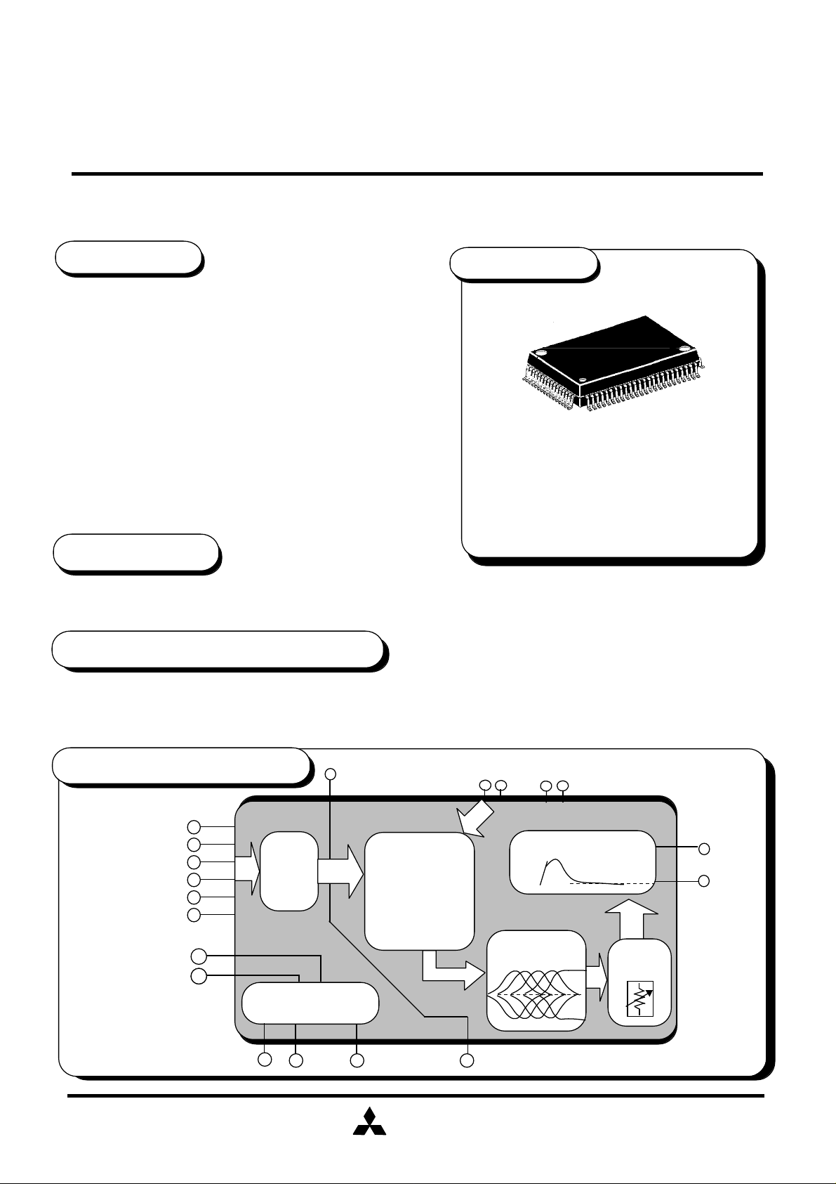
M62433FP
DIGITAL SOUND CONTROLLER
PACKAGE
Outline
Pitch : 0.8 mm
Size : 20.0 mm X 14.0mm
X 2.8mm
80P6N
APPLICATION
Home Audio equipment,Radio-Cassette tape recorder,TV
RECOMMENDED OPERATING CONDITIONS
Supply voltage range • • • • ±4.5 ~ ±7.3V
Rated supply voltage • • • • ±7 V
SYSTEM BLOCK DIAGRAM
IN A
IN B
IN C
IN D
IN E
IN F
PORTA
PORTB
6-Input
selector
RECOUT 2
(3-Outputs)
SW FOR:
Multilingual
switching
Vocal cancel
Surround
DPL and
other modes
KEY1 KEY2
Bass boost
Tone
OUT2
OUT1
Electric
volume
LATCH
µ -com Interface
DATA
CLK
MITSUBISHI
ELECTRIC
RECOUT1 (3-Outputs)
( / 2 1 )D - 62433Q - 78A
1
Page 2
MITSUBISHI SOUND PROCESSORS
PRELIMINARY
Notice ; This is not a final specification.
some parametric limits are subject to change.
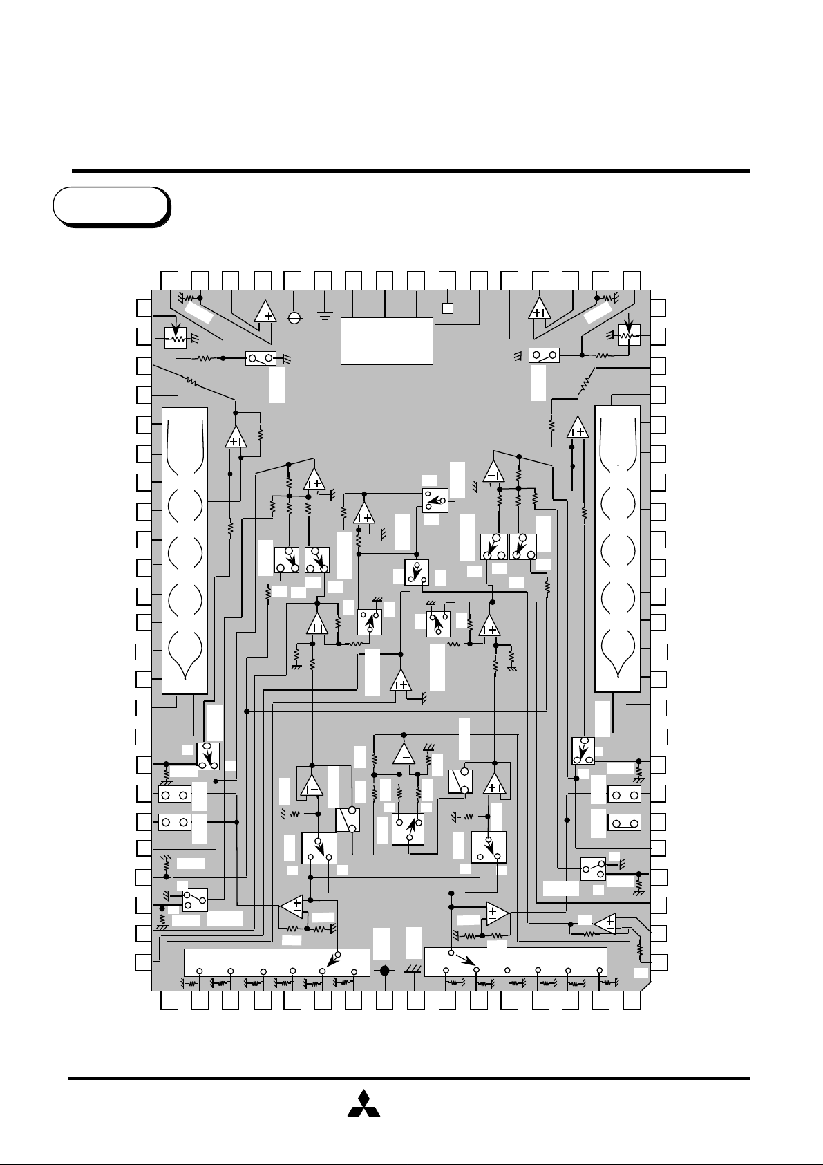
IC Internal
Block Diagram
BB2
BUFIN2
BUFNF2
BUFOUT2
40 39 38 37 36
VOLOUT2
FOUT2
F5F2
F4IN2
F4O2
F4F2
F3IN2
F3O2
F3F2
F2IN2
F2O2
F2F2
F1IN2
F1O2
F1F2
FIN2
REC2B
REC2A
REC2C
MIC IN
KEYOUT2
KEYIN2
BPFOUT
100K
41
42
43
444546
4748
49505152
SW18
5-Element Graphic Equalizer
53
54
55
56
57
58
100K
SW16
A
B
SW6SW4
59
6061
100K
B
A
626364
SW22 5K
100K
F
E
D
AVDD
SW20
A
B
100K
SW8
B
20K
C
DGND
35 34
G=2.4î{
A
B
SW12-1
8.5K
B
LATCH
33 32 31
µ -COM
SW10-2
A
SW12-2
20K
20K
A
A
DATA
interface
Logic
SW13
B
B
20K
A
SW9
SW2
CLOCK
A
B
A
B
SW11-2
20K
20K
B
SW1
A
DVDD
30
SW14
SW10-1
B
A
SW11-1
SW7
A
8.5K
B
M62433FP
DIGITAL SOUND CONTROLLER
PORTA
PORTB
BUFOUT1
29 28 27 26 25
SW19
G=2.4î{
SW17
A
100K
B
20K
C
A
B
SW21
E
D
BUFIN1
BUFNF1
100K
SW15
A
100K
B
SW5SW3
B
100K
A
F
BB1
VOLOUT1
VOLIN1VOLIN2
23 24
22
21
16 17 18 19 20
15
14
5-Element Graphic Equalizer
12 13
11
9 10
8
7
6
5
4
3
2
1
5K
FOUT11
F5F1
F4IN1
F4O1
F4F1
F3IN1
F3O1
F3F1
F2IN1
F2O1
F2F1
F1IN1
F1O1
F1F1
FIN1
REC1B
REC1A
REC1C
KEYOUT1
KEYIN1
P/S C
DELAY OUT
65 66 67 68 69 70 71 72 73 74
IN2F
BPFIN
IN2E
IN2D
IN2C
IN2B
IN2A
AVSS
AGND
MITSUBISHI
ELECTRIC
75 76
IN1A
IN1B
77
IN1C
78
IN1D
79 80
IN1E
IN1F
DELAYIN
( / 2 1 )D - 62433Q - 78A
2
Page 3
MITSUBISHI SOUND PROCESSORS
PRELIMINARY
Notice ; This is not a final specification.
some parametric limits are subject to change.
Pin Description
Pin No. Symbol Function
72
73
74,75,76
77,78,79
71,70,69
68,67,66
80
1
AVSS
AGND
IN1A,IN1B,IN1C
IN1D,IN1E,IN1F
IN2A,IN2B,IN2C
IN2D,IN2E,IN2F
DELAYIN
DELAYOUT
Negative power supply to internal analog circuit
Input pin at the side of channel1
Input pin at the side of channel2
M62433FP
DIGITAL SOUND CONTROLLER
GND of internal analog circuit
(R-L) output pin for surround. Connected to the input
of delay circuit. Total load resistance is 20kΩ
(R-L) input pin for surround.
Connected to the output of delay circuit.
2
3,63
4,62
64
65
5,60
6,59
7,58
8,57
9,46
10,45
P/S C
KEYIN1
KEYIN2
KEYOUT1
KEYOUT2
BPFOUT
BPFIN
REC1A
REC2A
REC1B
REC2B
REC1C
REC2C
FIN1
FIN2
F1F1
F1F2
F1O1
F1O2
Phase shift filter pin for surround
Key control adapter output pin. Connected to the input
of key control circuit etc. Total load resistance is 20kΩ
Key control adapter input pin.
Connected to the outputof key control circuit
Band-pass filter amplifier output pin for voice cancel
Band-pass filter amplifier input pin for voice cancel
Rec output pin A
Rec output pin B (with mute SW)
Rec output pin C (with mute SW)
Tone input pin (Surround adapter OUT)
Pin for connecting resonance impedance (band filter)
of the 1st element
Output pin of resonance buffer amplifier of the 1st element
total load
resistance ;
min. 20KΩ
11,54
12,53
13,52
F1IN1
F1IN2
F2F1
F2F2
F2O1
F2O2
Input pin of resonance buffer amplifier of the 1st element
Pin for connecting resonance impedance (band filter)
of the 2nd element
Output of resonance buffer amplifier of the 2nd element
MITSUBISHI
ELECTRIC
( / 2 1 )D - 62433Q - 78A
3
Page 4
MITSUBISHI SOUND PROCESSORS
PRELIMINARY
Notice ; This is not a final specification.
some parametric limits are subject to change.
Pin No. Symbol Function
14,51
15,50
16,49
17,48
18,47
19,46
20,45
21,44
22,43
23,42
24,41
25,40
26,39
27,38
28,37
F2IN1
F2IN2
F3F1
F3F2
F3O1
F3O2
F3IN1
F3IN2
F4F1
F4F2
F4O1
F4O2
F4IN1
F4IN2
F5F1
F5F2
FOUT1
FOUT2
VOLIN1
VOLIN2
VOLOUT1
VOLOUT2
BB11
BB12
BUFIN1
BUFIN2
BUFNF1
BUFNF2
BUFOUT1
BUFOUT2
Input pin of resonance buffer amplifier of the 2nd element
Pin for connecting resonance impedance (band filter)
of the 3rd element
Output pin of resonance buffer amplifier of the 3rd element
Input pin of resonance buffer amplifier of the 3rd element
Pin for connecting resonance impedance (band filter)
of the 4th element
Output pin of resonance buffer amplifier of the 4th element
Input pin of resonance buffer amplifier of the 4th element
Pin for connecting band filter of the 5th element
Tone output pin. Capacitor is combined for connection
with the next stage.
R-ladder volume input pin
R-ladder volume output pin
Bass boost capacitance connection pin.
Sets frequency characteristics.
+input pin of bass boost output amplifier
-input pin of bass boost output amplifier
Output pin of bass boost output amplifier
M62433FP
DIGITAL SOUND CONTROLLER
29
30
31
32
33
PORTA
PORTB
DVDD
CLOCK
DATA
Output of port A
Output of port B
Power supply to internal logic circuit
Clock input pin for serial data transfer
Input pin of control data.
Reads data at the rising edge of clock.
MITSUBISHI
ELECTRIC
( / 2 1 )D - 62433Q - 78A
4
Page 5
MITSUBISHI SOUND PROCESSORS
PRELIMINARY
Notice ; This is not a final specification.
some parametric limits are subject to change.
Pin No. Symbol Function
34
35
36
LATCH
DGND
AVDD
61 MIC IN
Input pin of latch signal. The circuit status changes
at the rising edge of latch signal.
GND pin of internal logic circuits
Positive power supply pin of internal analog circuits
Microphone input pin
M62433FP
DIGITAL SOUND CONTROLLER
MITSUBISHI
ELECTRIC
( / 2 1 )D - 62433Q - 78A 5
Page 6
MITSUBISHI SOUND PROCESSORS
PRELIMINARY
Notice ; This is not a final specification.
some parametric limits are subject to change.
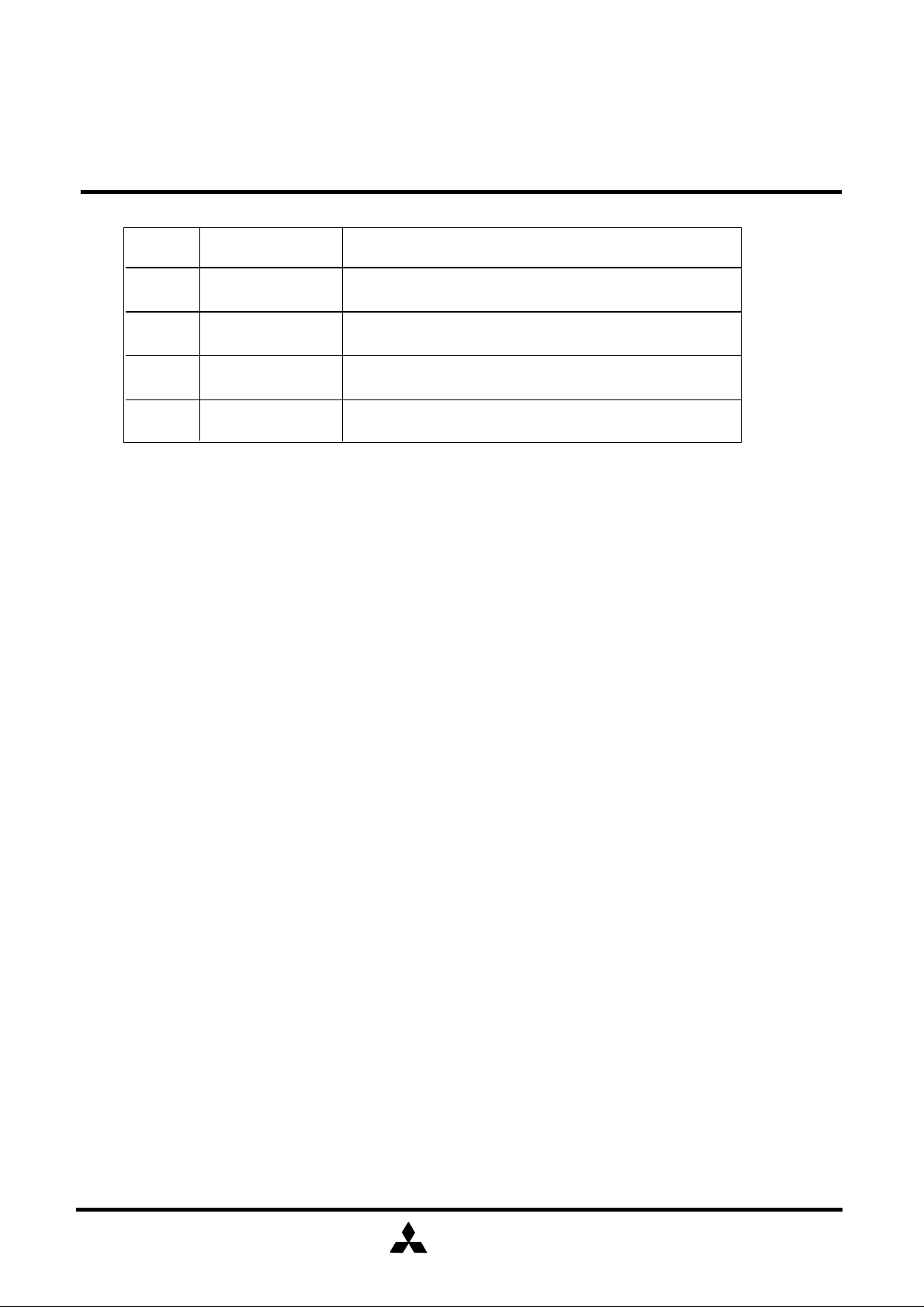
ABSOLUTE MAXIMUM RATINGS
Symbol
DVDD
Pd
K
Parameter Conditions Ratings Unit
Analog Power supplyAVDD,AVSS
Digital Power supply
Power dissipation
Thermal derating
Ta ≤ 25°C
Ta > 25°C
Attached PC Board*
M62433FP
DIGITAL SOUND CONTROLLER
±7.5
6.0
1370
13.7
V
V
mW
mW/°C
Topr
Tstg
Operating temperature
Storage temperature
Thermal derating
(Maximum ratings)
1.5
1.37W
1.0
0.5
Power dissipation pd [W]
685mW
-20 ~ +75
-55 ~ +125
*Note : PC Board
PC Board Size
140 mm X140 mm
PC Board Thickness
1.6 mm
PC Board Material
Epoxy
Copper Film Thickness
18 µm
Copper Foil Size
0.25 mm X 50 mm
°C
°C
0
0
25 50 75 100
Ambient Temperature Ta [°C ]
125
MITSUBISHI
ELECTRIC
150
( / 2 1 )D - 62433Q - 78A
6
Page 7
MITSUBISHI SOUND PROCESSORS
PRELIMINARY
Notice ; This is not a final specification.
some parametric limits are subject to change.
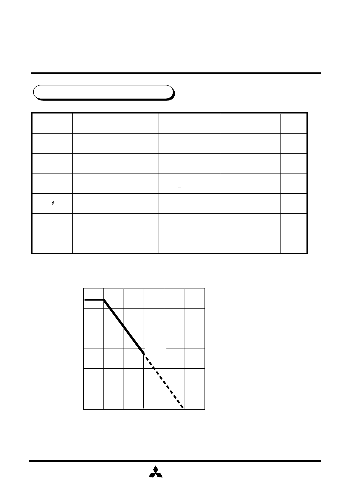
RECOMMENDED OPERATING CONDITIONS
( Ta=25°C, unless otherwise noted )
Analog (+) power supply
Analog (-) power supply
Digital power supply
SymbolParameter Conditions
AVDD
AVSS
DVDD
Note 1
Note 1
DVDD≤AVDD
MIN
4.5
-4.5 -7.0 -7.3
4.5
M62433FP
DIGITAL SOUND CONTROLLER
TYP
7.0
MAX
7.3
5.0 5.5
Unit
V
V
V
Logic
” H ” Level
VIH
input voltage
Logic
” L ” Level
VIL
input voltage
Note 1: The sequence of the power supply is as follows.
AVDD AVSS DVDD
TIMING DIAGRAM
H
DATA
CLOCK
D0
L
H
L
D1
VDDDVDD-0.7
0
DGND+0.7
V
V
Latch Signal
D7D6
D0
LATECH
H
L
DATA reading mode;
The rising edge of the CLOCK signal
MITSUBISHI
ELECTRIC
LATCH reading mode;
The rising edge of the LATCH signal
( / 2 1 )D - 62433Q - 78A
7
Page 8

MITSUBISHI SOUND PROCESSORS
PRELIMINARY
Notice ; This is not a final specification.
some parametric limits are subject to change.
CLOCK DATA TIMING
CLOCK
75%
25%
t r t f
WHC
t
75%
M62433FP
DIGITAL SOUND CONTROLLER
c r
t
WLC
t
DATA
25%
t r
t t
LATCH
DIGITAL CIRCUIT AC CHARACTERISTICS
t c r
t W H C
t W L C
t r
t f
t S D
t H D
t S L
t W H L
C L O C K c y c l e t i m e
C L O C K p u l s e w i d t h ( ” H ” l e v e l )
C L O C K p u l s e w i d t h ( ” L ” l e v e l )
C L O C K , DATA , LATCH r i s e t i m e
C L O C K , DATA , LATCH f a l l t i m e
DATA s e t u p t i m e
DATA h o l d t i m e
LATCH s e t u p t i m e
LATCH p u l s e w i d t h
S D H D
t f
WHC
t r
S L
t
Limits
Min
typ
4
1.6
1.6
0.8
0.8
1
1.6
t
Max
0.4
0.4
UnitSymbol Parameter
µ sec
t f
75%
25%
MITSUBISHI
ELECTRIC
( / 2 1 )D - 62433Q - 78A
8
Page 9

MITSUBISHI SOUND PROCESSORS
PRELIMINARY
Notice ; This is not a final specification.
some parametric limits are subject to change.
DATA FORMAT
4 patterns input formats can be selected by setting D6 and D7.
( When the IC is powered up, the internal settings are not fixed. )
( 1 )
( 2 )
DO1 D11 D21 D31 D41 D51
Rec out A
S W 3,4
1 : Mute
0 : Pass
Rec out B
S W 5,6
1 : Mute
0 : Pass
For the multiplex softwere
S W 7 S W 8
1 : A side
0 : B side
DO2 D12 D22 D32 D42 D52 D6 D7
S W 11-1,2
S W 12-1,2
1:Aside/ON
0:Bside/OFF
S W 13
1 : A side
0 : B side
S W 21,22
1 : A side
0 : B side
1 : A side
0 : B side
S W 14
1 : A side
0 : B side
S W 9
1 : A side
0 : B side
S W 17,18
1 : A side
0 : B side
M62433FP
DIGITAL SOUND CONTROLLER
D6 D7
S W 10-1
S W 10-2
1 : ON
0 : OFF
S W 15,16
1 : A side
0 : B side
0 0
0 1
( 3 )
( 4 - 1 )
( 4 - 2 )
DO3 D13 D23 D33 D43 D53 D6 D7
For Tone control (element)
Refer to the Tone Control 1 Code
Bass Boost SW15,16 A / B
For Tone control (gain)
Refer to the Tone Control 2 Code
1 0
DO4-1 D14-1 D24-1 D34-1 D44-1 D54-1 D6-1 D7-1
For Master Volume
Refer to the Master Volume Code
DO4-2 D14-2 D24-2 D34-2 D44-2
For Input selector
Refer to the Input selector Code
0
D54-2
1
1 1
D6-2 D7-2
1 1
( 6 ) Tone control 2 code (gain)
( 5 ) Tone control 1 code (element)
Tone 1 (F1)
Tone 2 (F2)
Tone 3 (F3)
Tone 4 (F4)
Tone 5 (F5)
Boost
D03 D13
0 10
0
1
10
01 0
1 1
ONBass
0
11 0
11 1OFF
D23
0
1
+0 dB
+3 dB
+6 dB
Boost
+9 dB
-0 dB
-3 dB
Cut
-6 dB
-9 dB
D33 D43
0
0
0
0
1
1
1
1
D53
0
0
1 0
1 1
0 0
0 1
1 0
1 1
0
1
MITSUBISHI
ELECTRIC
( / 2 1 )D - 62433Q - 78A
9
Page 10

MITSUBISHI SOUND PROCESSORS
PRELIMINARY
Notice ; This is not a final specification.
some parametric limits are subject to change.
( 7 )Master volume code
A T T
— 0 . 0 d B
— 2 . 0 d B
— 4 . 0 d B
— 6 . 0 d B
— 8 . 0 d B
— 1 0 . 0 d B
— 1 2 . 0 d B
— 1 4 . 0 d B
— 1 6 . 0 d B
— 1 8 . 0 d B
— 2 0 . 0 d B
— 2 2 . 0 d B
— 2 4 . 0 d B
— 2 6 . 0 d B
— 2 8 . 0 d B
— 3 0 . 0 d B
— 3 2 . 0 d B
— 3 4 . 0 d B
— 3 6 . 0 d B
— 3 8 . 0 d B
— 4 0 . 0 d B
— 4 4 . 0 d B
— 4 8 . 0 d B
— 5 2 . 0 d B
— 5 6 . 0 d B
— 6 0 . 0 d B
— 6 4 . 0 d B
— 6 8 . 0 d B
— 7 2 . 0 d B
— 7 6 . 0 d B
— 8 0 . 0 d B
— ∞
D04 D14
0 0 0
1 0 0 0
1 0 0 00
1
1 0 0
0 0 1 0 0
1 0 1 0 0
0 1 1 0 0
1 1 1 0 0
0 0 0 1 0
1 0 0
0 1 0 1 0
1 1 0 1 0
0 0 1 1 0
1 0 1 1 0
0 1 1 1
1 1 1 1
0 0 0 0 1
1 0 0 0 1
0 1 0 0 1
1 1 0 0 1
0 0 1 0 1
1 0 1 0 1
0 1 1 0 1
1 1 1 0 1
0 0 0 1 1
1 0 0 1 1
0 1 0 1 1
1 1 0 1 1
0 0 1 1 1
1 0 1 1 1
0 1 1 1 1
1 1 1 1 1
D24
D34
0
1
D44
0
0
0
0
0
0
M62433FP
DIGITAL SOUND CONTROLLER
( 8 ) Port output code
DATA
D 32-2
D 44-2
( 9 ) Multilingual record code
Normal
Lch only
Rch only
R/L Exchange
( 10 ) Input selector code
Selector
A
B
C
D
E
F
All off
Port output
0
Port A : L
1
Port A : H
0
Port B : L
1
Port B : H
D21 D31
0
0
1
1
D14-2
D14-2 D24-3
0
0
0
0
1
1
1
0
1
0
1
0
0
1
1
0
1
1
0
1
0
1
0
0
1
( 11 ) The others code
For voice cancel
D41=1
D02=1
SW9 : A side
SW11,12-1 : ON
SW11,12-2 : A side
D12=0
D32=0
For Surround
D41=0
D02=1
SW13 : B side
SW14 : B side
SW9 : B side
SW11,12-1 : ON
SW11,12-2 : A side
D12=1
D32=1
SW13 : A side
SW14 : A side
MODE
NORMAL
STEREO
STEREO
+ MIC
MIX MODE
Source
+ Key control
( )
KEY CONTROL
MODE
DPL MODE
MITSUBISHI
ELECTRIC
SW21,22 SW17,18
B side
B side
A side
A side
B side
B side
A side
A side
A side
B side
SW10-1
SW10-2
B side
B side
B side
A side
A side
( / 2 1 )D - 62433Q - 78A
SW15,16
B side
B side
B side
B side
A side
1 0
Page 11

MITSUBISHI SOUND PROCESSORS
PRELIMINARY
Notice ; This is not a final specification.
some parametric limits are subject to change.
ELECTRICAL CHARACTERISTICS
( Ta=25°C,AVDD=7.0V,AVSS=-7.0V,DVDD=5.0V ,f=1kHz
Tone control & Bass Boost setting :0dB , unless otherwise noted )
( 1 ) Power supply
Parameter
Circuit current (Analog +)
Circuit current (Analog -)
Circuit current (Digital )
Symbol
AIdd
AIss
DIdd
Conditions
AVDD=7.0V, AVSS= -7.0V
ISINK of 36pin
No signal input
AVDD=7.0V, AVSS= -7.0V
ISOURCE of 72pin
No signal input
DVDD= 5V
ISINK of 31pin
No signal input
M62433FP
DIGITAL SOUND CONTROLLER
Min
-48
Limits
typ
40 mA
-40
0.5
Max
48
1.0
Unit
mA
mA
( 2 ) Input/Output
Parameter
Input impedance
Maximum input voltage
Output terminal voltage
I/O voltage gain
Output noise voltage
Distortion
Channel separation
Symbol
Rin
VIM
Vodc
Vrecdc
Gv
Vono
Vrecno
THD
THDrecB,C
CT
CTrec
Conditions
66 ~ 71pin,74 ~ 79Pin,Ta=25°C
(66 ~ 71pin input),(74 ~ 79pin input)
28,37pin output
RL =4.7KΩ , THD=1%
28pin,37pin,No input signal
5pin,60pin, No input signal
Vin=1Vrms,FLAT,(66 ~ 71Pin),
(74 ~ 79Pin)-28,37Pin
28,37pin
JIS-A filter
No ininput signal
Rg=10KΩ
FLAT
28pin,37pin, BW=400 ~ 30kHz
Vi= -20dBv , RL=4.7KΩ
(6,59pin),(7,58pin),BW400 ~ 30kHz
Vi=-20dBv , RL=20KΩ
Vo=0.5Vrms , RL=4.7KΩ,JIS-A
28pin—37pin Rg=0KΩ, 61pin GND
Vo=0.5Vrms , RL=20KΩ,JIS-A
6pin—59pin Rg=0KΩ, 61pin GND
ATT0
ATTM
6,59pin
7,58pin
Min
-0.1
-0.1
10.0
Limits
typ
Max
47
10020
4.0 Vrms3.0
0
0.1
0
12.0
14.0
70.0
55.0
5.0
0.01
0.05
-75 -55
-75 -55
0.1
15
3020.0
Unit
KΩ
V
V
dB
µ Vrms
µ Vrms
µ Vrms
%
%0.050.01
dB
dB
MITSUBISHI
ELECTRIC
( / 2 1 )D - 62433Q - 78A
1 1
Page 12

MITSUBISHI SOUND PROCESSORS
PRELIMINARY
Notice ; This is not a final specification.
some parametric limits are subject to change.
( 3 ) Tone Control
Parameter
Voltage gain
(Tone control)
Balance between channels
Symbol
Gboost1
Gboost2
Gboost3
Gcut1
Gcut2
Gcut3
BALton 0 +1.5-1.5
M62433FP
DIGITAL SOUND CONTROLLER
Conditions
3dB
6dB
f=1KHz,Vo=1Vrms
10dB
-3dB
-6dB
-10dB
f=1KHz,Vo=1Vrms,
Input;8,57Pin Output;22,43Pin
+10dB and -10dB
Input ;8pin,57pin
Output ;22pin,43pin
Limits
typ
Min
1.5 4.5
4.5 7.5
8.0 12.0
-4.5 -1.5
-7.5 -4.5
-12.0 -8.0
Max
3
6
10
-3
-6
-10
Unit
dB
dB
dB
dB
dB
dB
dB
( 4 ) Bass Boost
Parameter
Voltage gain
(Bass boost)
Balance between channels
( 5 ) PORT OUTPUT
Parameter
Minimum "H" voltage
Maximum "L" leak current
Symbol
f=70Hz,Vo=0.5Vrms
Input ; 23,42pin
Output ; 27,38pin
f=70Hz ,Vo=0.5Vrms
BALton 0 +2.0-2.0 dB
Input ; 23,42Pin
Output ; 27,38pin,
Symbol
VpHA
VpHB
IpLA
IpLA
Conditions
Bass boost ON
Conditions
RL=1.8kΩ
Limits
Min
Min
typ
Max
-10 -2 dB
5.4 V
-6Gboost
Limits
typ
Max
6.0
0-3 uA
3
Unit
Unit
Maximum drive current IpD
MITSUBISHI
ELECTRIC
0.7 mA3
( / 2 1 )D - 62433Q - 78A 1 2
Page 13

MITSUBISHI SOUND PROCESSORS
PRELIMINARY
Notice ; This is not a final specification.
some parametric limits are subject to change.
Master volume circuit
— 0 d B
5968
3084
CL
1605
3477
2758
2192
1739
1383
1097
3016
2396
1903
1512
1200
954
758
11723
9312
7533
5740
4667
3707
2945
4197
2648
1671
1054
665.5
1357
857.8
540.5
342
214.2
262.5
— 2 d B
— 4 d B
— 6 d B
— 8 d B
—1 0 d B
—1 2 d B
—1 4 d B
—1 6 d B
—1 8 d B
—2 0 d B
—2 2 d B
—2 4 d B
—2 6 d B
—2 8 d B
—3 0 d B
—3 2 d B
—3 4 d B
—3 6 d B
—3 8 d B
—4 0 d B
—4 4 d B
—4 8 d B
—5 2 d B
—5 6 d B
—6 0 d B
—6 4 d B
—6 8 d B
—7 2 d B
—7 6 d B
—8 0 d B
—∞
DIGITAL SOUND CONTROLLER
+
-
Master volume code
A T T
— 0 . 0 d B
— 2 . 0 d B
— 4 . 0 d B
— 6 . 0 d B
— 8 . 0 d B
—1 0 . 0 d B
—1 2 . 0 d B
—1 4 . 0 d B
—1 6 . 0 d B
—1 8 . 0 d B
—2 0 . 0 d B
—2 2 . 0 d B
—2 4 . 0 d B
—2 6 . 0 d B
—2 8 . 0 d B
—3 0 . 0 d B
—3 2 . 0 d B
—3 4 . 0 d B
—3 6 . 0 d B
—3 8 . 0 d B
—4 0 . 0 d B
—4 4 . 0 d B
—4 8 . 0 d B
—5 2 . 0 d B
—5 6 . 0 d B
—6 0 . 0 d B
—6 4 . 0 d B
—6 8 . 0 d B
—7 2 . 0 d B
—7 6 . 0 d B
—8 0 . 0 d B
—∞
D04 D14
0 0 0
1
1
0 0 1 0 0
1 0 1
0 1 1 0 0
1 1 1
0 0 0 1 0
1 0 0 1
0 1
1 1 0 1 0
0 0 1 1 0
1
0 1 1 1
1 1 1 1
0 0
1 0
0
1 1
0 0 1 0 1
1 0 1 0 1
0 1 1 0 1
1 1 1
0 0 0 1 1
1 0 0 1 1
0 1 0 1 1
1 1 0 1 1
0 0 1 1 1
1 0 1 1 1
0 1 1 1 1
1 1 1 1 1
M62433FP
D24
0
1 0 0 00
1 0
0
1 0
0 0
0
1
0
0
0
D34
0
0
0
0 0
1
1
0
0 1
0
0 1
0 1
D44
0
0
0
0
0
0
0
0
0
1
1
MITSUBISHI
ELECTRIC
( / 2 1 )D - 62433Q - 78A
1 3
Page 14

MITSUBISHI SOUND PROCESSORS
PRELIMINARY
Notice ; This is not a final specification.
some parametric limits are subject to change.
Function description
( 1 ) Voice cancel block equivalent circuit
( L + C ) ( h + m + l )
( R + L + 2 C ) ( h + m + l )
+
BPF/
-6dBATT
M62433FP
DIGITAL SOUND CONTROLLER
L ( h + m / 2 + 1 )
+ C ( h + 1 ) —R m / 2
—
( R + L + 2 C ) m / 2
( R + C ) ( h + m + l )
( 2 ) Surround block equivalent circuit
L + C
R — L
R + C
—
Pass
or
Delay
—
—
+
R ( h + m / 2 + 1 )
+ C ( h + 1 ) —L m / 2
2 L — R + C
2 R — L + C
MITSUBISHI
ELECTRIC
( / 2 1 )D - 62433Q - 78A
1 4
Page 15

MITSUBISHI SOUND PROCESSORS
PRELIMINARY
Notice ; This is not a final specification.
some parametric limits are subject to change.
( 3 ) Tone control equivalent circuit
R3
FBASS
C1
OUT
BASS
R1
M62433FP
DIGITAL SOUND CONTROLLER
Center frequency
f0 = 1 / 2π C1 • C2 • R1 • R2 [Hz]
Q = ( C2 • R2 ) / C1 ( C1+R1 )
C2
INBASS
R2
Fig.1 The equivalent circuit of tone controller
C1
L
R1
R2
Example; Bass band ( f=150Hz )
R1=1.5KΩ, R2=56KΩ
C1=1.5 µ, C2=0.01 µ
F1 F2 F3 F4 F5
1.0k
300k
Fig.2 is equivalent to Fig.1
To convert component constants,
the equation below is used.
L=C2 • R1 • R2
1.0k
300k
1.0k
300k
1.0k
150k
R1
Fig.12 The equivalent circuit using L
MITSUBISHI
ELECTRIC
( / 2 1 )D - 62433Q - 78A
1 5
Page 16

MITSUBISHI SOUND PROCESSORS
PRELIMINARY
Notice ; This is not a final specification.
some parametric limits are subject to change.
( 4 ) Bass boost equivalent circuit
12.6K
ZL
5.97K
RL=
3.08K
1.6K
CL
11.7K
55.8K
3.57K
M62433FP
DIGITAL SOUND CONTROLLER
57K
Bass Boost loudness equivalent circuit (Center tup type)
Regard "RL+ " as "ZL"
1
÷CL
Next formula show the frequency characteristic.
5 . 9 7 K / / [ 1 1 .7 K + Z L / / 5 7 K ]
1 2 . 6 K + 5 . 9 7 K / / [ 1 1 . 7 K + Z L / / 5 7 K ]
G v = 2 0 Log
Z L / / 5 7 K
[
1 1 . 7 K + Z L / / 5 7 K
When a frequency is enough low ,
G v = 2 0 Log
5 7 K
[ ]
1 1 . 7 K + 5 7 K
5 . 9 7 K / / [ 1 1 . 7 K + 5 7 K ]
1 2 . 6 K + 5 . 9 7 K / / [ 1 1 . 7 K + 5 7 K ]
When a frequency is enough high ,
G v = 2 0 Log
3 . 0 8 K / / 5 7 K
[
1 1 . 7 K + 3 . 0 8 K / / 5 7 K
-12dB
5 . 9 7 K / / [ 1 1 . 7 K + 3 . 0 8 K / / 5 7 K ]
1 2 . 6 K + 5 . 9 7 K / / [ 1 1 . 7 K + 3 . 0 8 K / / 5 7 K ]
]
= —1 1 . 9 d B
÷0=16.8K • CL
f=100Hz CL=0.1 µF
= —2 6 d
]
B
Gain
-26dB
100Hz
frequency
MITSUBISHI
ELECTRIC
VOL-26 dB
( / 2 1 )D - 62433Q - 78A
1 6
Page 17

MITSUBISHI SOUND PROCESSORS
PRELIMINARY
Notice ; This is not a final specification.
some parametric limits are subject to change.
( 3 ) Band-Pass filter block equivalent circuit
C 1
20K
20K
C 2
( The equation for band-pass filter )
10K
M62433FP
DIGITAL SOUND CONTROLLER
0 d B
— 3 d B
f L
f H
f H [ cut-off frequency ]
High frequency's side
f L [ cut-off frequency ]
Low frequency's side
1
2 π C 1 • 1 0 K
1
2 π C 2 • 1 0 K
MITSUBISHI
ELECTRIC
( / 2 1 )D - 62433Q - 78A
1 7
Page 18

MITSUBISHI SOUND PROCESSORS
PRELIMINARY
Notice ; This is not a final specification.
some parametric limits are subject to change.
KEYIN2
SELECT OUT 2
KEYIN2
0 dB
20KΩ
20KΩ
20KΩ
amp 12
- 6 dB
20KΩ
sw12-2
A
B
amp 24
sw13
B
M62433FP
DIGITAL SOUND CONTROLLER
KEYIN1
KEYIN1
20KΩ
20KΩ
20KΩ
sw11-2
B
sw14
20KΩ
A
B
A
A
0 dB
amp 2
- 6 dB
20KΩ
SELECT OUT1
20KΩ
BPFOUT
0 dB
DELAYIN
sw12-1
C
D
20KΩ
20KΩ
E
F
sw2
B
A
amp 11
A
B
90KΩ
sw8
The block diagram along the signal flow (No.1)
—6dB
amp 21
A
sw9
0 dB
amp 22
BPFIN
0 dB
20KΩ
B
amp 23
PHEIZE SHIFTER
0 dB
20KΩ
F
sw11-1
E
D
amp 1
90KΩ
sw7
B
A
sw1
C
B
A
100KΩ
100KΩ
IN 2A
IN 2B
IN 2C
IN 2D
IN 2E
MITSUBISHI
IN 2F
IN 1F
IN 1E
IN 1D
IN 1C
( / 2 1 )D - 62433Q - 78A
1 8
IN 1B
IN 1A
ELECTRIC
Page 19

MITSUBISHI SOUND PROCESSORS
PRELIMINARY
Notice ; This is not a final specification.
some parametric limits are subject to change.
REC2C
TONEIN2
100K
B
A
sw16
DPL
(Rch)
REC2A
REC2B
12.5K
sw6
sw4
sw10-2
B
A
amp 13
B
30K
5.0K 5.0K
sw18b
A
30K
sw17b
A
M62433FP
DIGITAL SOUND CONTROLLER
REC1C
TONEIN1
100K
A
B
sw15
DPL
(Lch)
B
amp 3
12.5K
A
sw10-1
B
REC1A
sw3
REC1B
sw5
5.0K
sw22
20K
amp 20
8.5K
B
Key
Con
KEYIN2
A
100KΩ
The block diagram along the signal flow (No.2)
SELECT OUT 2
KEYIN2
MIC AMP
5.0K
sw21
20K
amp 10
8.5K
SELECT OUT 1
Key
B
100KΩ
Con
100KΩ
A
KEYIN1
KEYIN1
MITSUBISHI
ELECTRIC
( / 2 1 )D - 62433Q - 78A
1 9
Page 20

MITSUBISHI SOUND PROCESSORS
PRELIMINARY
Notice ; This is not a final specification.
some parametric limits are subject to change.
OUT 2
10µ
-
+
10µ
100kΩ
amp 15
M62433FP
DIGITAL SOUND CONTROLLER
OUT 1
10µ
amp 5
0dB ~ -∞
( 32 steps )
10µ
FOUT2
400Ω
10KΩ
The block diagram along the signal flow (No.3)
each frequency change +10dB ~ -10dB
-
+
10KΩ
amp 14
24.2K
22.7K
22.7K
8.55K
4.62K
22.7K
8.55K
22.7K
3.12K
8.55K
8.55K
3.12K
10.0K
3.12K
56K
4.62K
56K
1.5K
OFF : Bass Boost ON
ON : Normal
amp 4
amp 19
amp 18
amp 17
amp 16
The same channel2
amp 9
amp 8
amp 7
amp 6
MITSUBISHI
ELECTRIC
( / 2 1 )D - 62433Q - 78A 2 0
Page 21

MITSUBISHI SOUND PROCESSORS
PRELIMINARY
Notice ; This is not a final specification.
some parametric limits are subject to change.
Application
10µ
+
560p
10µ
2700p
680p
0.027µ
0.001µ
0.082µ
0.033µ
0.27µ
0.1µ
+
BUFOUT2
+
+
2k2k
40 39 38 37 36
100K
41
42
43
44
45
4647
48
49
50515253
SW18
5-Element Graphic Equalizer
digital GND
analog 7V
35 34
SW20
G=2.4î{
A
A
B
M62433FP
DIGITAL SOUND CONTROLLER
5V
MCU
PORTB
10k10k
33 32 31 30 29 28 27 26 25
µ -COM
interface
Logic
G=2.4î{
A
SW14
B
SW10-2
B
A
SW13
B
B
B
A
SW10-1
B
A
A
BUFOUT1
+
PORTA
2k
SW19
SW17
A
B
+
2k
10µ
+
0.1µ
560p
100K
24
23
10µ
+
2700p
680p
19 20 21 22
0.027µ
18
0.001µ
0.082µ
0.033µ
5-Element Graphic Equalizer
0.27µ
12 13 14 15 16 17
0.01µ
0.82µ
DPL2
REC2B
REC2A
REC2C
MIC IN
20k
1000p
10k
54555657
58
59606162
63
64
65 66
SW1
73 74
-7V
analog
SW11-2
20K
20K
B
A
GND
analog
SW11-1
100K
SW7
A
8.5K
20K
C
B
75 76 77 78 79 80
IN1A
IN1B
SW12-2
SW16
A
100K
100K
B
A
100K
B
SW6
SW4
SW22 5K
F
E
100K
SW8
B
8.5K
20K
D
C
67 68 69 70 71
20k
0.15µ
IN2F
IN2E
IN2D
IN2C
SW12-1
B
A
A
IN2B
20K
20K
20K
A
SW9
SW2
72
IN2A
11
0.01µ
10
0.82µ
SW15
A
100K
B
SW5
SW3
B
B
SW21
A
100K
9
DPL1
7 8
6
5
REC1B
REC1A
REC1C
4
3
2
D
IN1C
E
IN1D
F
IN1E
IN1F
1
5K
470p
Key control IC
20K
OR DPL
MITSUBISHI
ELECTRIC
( / 2 1 )D - 62433Q - 78A
2 1
 Loading...