

Page 1
MITSUBISHI<Dig.Ana.INTERFACE>
2
64 channels control.
MONITOR or CTV.
CHIP SELECT
8bit Latch
segment R-2R
8bit Latch
segment R-2R
8bit Latch
8bit Latch
8bit Latch
segment R-2R
8bit Latch
segment R-2R
8bit Latch
segment R-2R
8bit Latch
segment R-2R
9
11
161213141517181920102
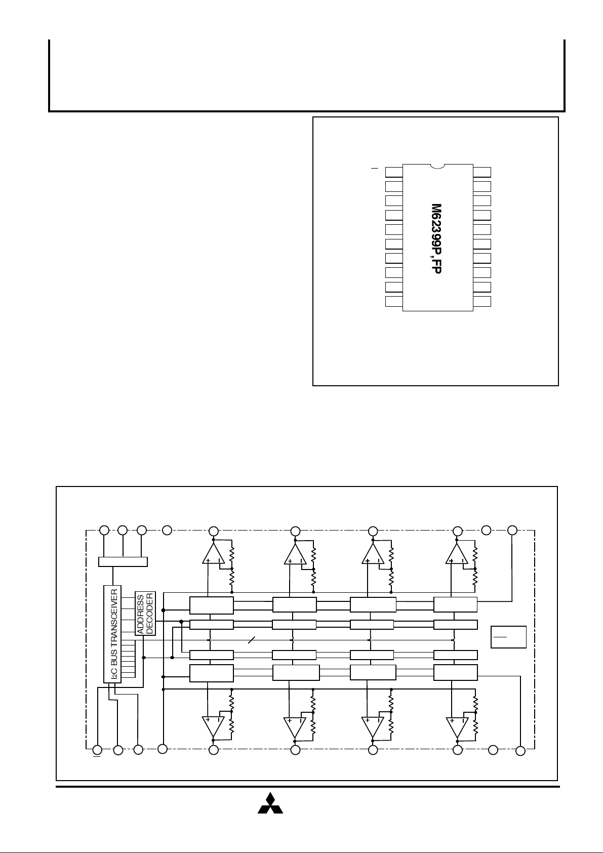
M62399P,FP
8-BIT 8CH I C-BUS D-A CONVERTER WITH BUFFER AMPLIFIERS
DESCRIPTION
The M62399P,FP is an integrated circuit semiconductor of
high voltage type CMOS structure with 8 channels of built-in DA converters with output buffer operational amplifiers.
The input is 2-wires serial method is used for the transfer
formal of digital data to allow connection with a microcomputer
with minimum wiring.
The output buffer operational amplifier employs AB class
output circuit with sync and source drive capacity of 2.5mA or
more,and it operates in the whole voltage range from VrefU to
ground.
And because of connects maximum 8 pieces,it is possible to
FEATURES
•Digital data transfer format
I C-bus serial data method
•Output buffer operational amplifier
it operates in the whole voltage range from VrefU(0~12V)to
ground.
•High output current drive capacity
±2.5mA over
•Preparation two high level reference voltage terminal
because there are two high level reference voltage
terminal,it can set up two kinds differ voltage range.
APPLICATION
Conversion from digital control data to analog control data
for home-use and industrial equipment.
Signal gain control or automatic adjustment of DISPLAY-
PIN CONFIGURATION (TOP VIEW)
20
19
18
17
165
156
147
138
129
1110
SCL
SDA
Ao5
Ao6
Ao7
Ao8
VrefL
VrefU1
GND
1
R
2
3
4
Outline 20P4(P)
20P2N-A(FP)
CS0
CS1
CS2
VDD
Vcc
Ao4
Ao3
Ao2
Ao1
VrefU2
BLOCK DIAGRAM
2 3
1
SDA
SCL
R
VrefL
VrefU2Ao1Ao2Ao3Ao4VDDCS2CS1CS0
Vcc
R2
R1
8
8bit upper
8bit upper
segment R-2R
8bit upper
8bit upper
R1
R2
8
4 5 6 7
R2
R1
R1
R2
8bit upper
8bit upper
segment R-2R
R2
R1
8bit upper
8bit upper
R1
R2
Ao5 Ao6 Ao7 Ao8 VrefU1
R2
R1
R1
R2
GND
R2
R1
=2.4
MITSUBISHI
ELECTRIC
( / 5 )
1
Page 2
2
EXPLANATION OF TERMINALS
Pin No.
3
1
2
12
13
14
15
4
5
6
7
16
17
10
8
9
11
18
19
20
Symbol
SDA
R
SCL
Ao1
Ao2
Ao3
Ao4
Ao5
Ao6
Ao7
Ao8
VCC
VDD
GND
VrefL
VrefU1
VrefU2
CS2
CS1
CS0
MITSUBISHI<Dig.Ana.INTERFACE>
M62399P,FP
8-BIT 8CH I C-BUS D-A CONVERTER WITH BUFFER AMPLIFIERS
Function
Serial data input terminal
Reset signal input terminal
Serial clock input terminal
8-bit D-A converter output terminal
Analog power supply terminal
Digital power supply terminal
Analog and digital common GND
D-A converter low level reference voltage input terminal
D-A converter high level reference voltage input terminal 1
D-A converter high level reference voltage input terminal 2
Chip select data input terminal 2
Chip select data input terminal 1
Chip select data input terminal 0
MITSUBISHI
ELECTRIC
( / 5 )
2
Page 3

MITSUBISHI<Dig.Ana.INTERFACE>
2
M62399P,FP
8-BIT 8CH I C-BUS D-A CONVERTER WITH BUFFER AMPLIFIERS
ABSOLUTE MAXIMUM RATINGS
Symbol Ratings
VCC
VDD
VrefU1,2 D-A converter upper reference voltage
VIND
Topr
Tstg
Supply voltage
Supply voltage
Digital input voltage
Operating temperature
Storage temperature
Parameter
ELECTRICAL CHARACTERISTICS
Digital part(Vcc=13V,VDD=VrefU1,2=+5V±10%,GND=VrefL=0V,Ta=-20 ~ +85°C,unless otherwise noted)
Symbol
VDD
IDD
IILK
VIL
VIH
Supply voltage
Supply current CLK=1MHz operation IAO=0µA
Input leak current
Input low voltage
Input high voltage
Parameter
VIN=0~VDD
Conditions
Test conditions
Min.
4.5
0.8VCC
-0.3~+13.5
-0.3~+7.0
VDD
-0.3~VDD+0.3
-20~+85
-40~+125
Limits
Typ.
5.0
Max.
5.5
1
10-10
0.2VCC
Unit
V
V
V
V
°C
°C
Unit
V
mA
µA
V
V
Analog part(Vcc=13V,VDD=VrefU1,2=+5V±10%,GND=VrefL=0V,Ta=-20 ~ +85°C,unless otherwise noted)
Symbol
Vcc
Icc
IrefU
VrefU
VrefL
VAO
IAO
SDL
SL
SZERO
SFULL
Eo
SR
Parameter
Supply voltage
Circuit current
D-A converter upper reference
voltage input current
D-A converter upper reference
voltage range
D-A converter lower reference
voltage range
Buffer amplifier output voltage range
Buffer amplifier output drive range
Differential nonlinearity error
Nonlinearity error
Zero code error
Full scale error
Gain error
Output slew rate
Test conditions
CLK=1MHz operation IAO=0µA
VrefU=5V VrefL=0V
Data condition:at maximum current
The output does not necessarily be the
values within the reference voltage setting
range.
IAO=±500µA
IAO=±1.0mA
Upper side saturation voltage=0.3V
Lower side saturation voltage=0.2V
VrefU=4.79V
VrefL=0.95V
Vcc=5.5V(15mV/LSB)
without load(IAO=0)
Min.
VDD
3.5
GND 1.5
0.2
-2.5
-1.0
-1.5
-2.0
-2.0
-3.0
Limits
Typ.
2.0 4.0
1.2
0.2
Max.
13
2.5
VDD
Vcc-0.10.1
Vcc-0.2
2.5
1.0
1.5
2.0
2.0
3.0
Unit
V
mA
mA
V
V
V
mA
LSB
LSB
LSB
LSB
%
V/µs
MITSUBISHI
ELECTRIC
( / 5 )
3
Page 4

MITSUBISHI<Dig.Ana.INTERFACE>
2
2
M62399P,FP
8-BIT 8CH I C-BUS D-A CONVERTER WITH BUFFER AMPLIFIERS
I C-BUS LINE CHARACTERISTICS
Symbol
fSCL
tBUF
tHD:STA Hold time start condition.After this period.The first clock pulse is generated
tLOW
tHIGH
tSU:STA
tHD:DAT
tSU:DAT
tR
tF
tSU:STO
*Note that transmitter must internally at reset a hold time to bridge the undefined region(max.300ns)of the falling edge of SCL.
SCL clock frequency
Time the bus must be free before a new transmission can start
The low period of the clock
The high period of the clock
Set up time for start condition(only relevant for a repeated start condition)
Hold time data
Set up time data
Rise time of both SDA and SCL lines
Fall time of both SDA and SCL lines
Set up time for stop condition
Parameter
Normal mode
Min Max
0
4.7
4.0
4.7
4.0
4.7
0
250
4.0
Max
100
1000
300
High speed mode
Min
0
1.3
0.6
1.3
0.6
4.7
0
100
20
20
0.6
400
0.9
300
300
Unit
KHz
µs
µs
µs
µs
µs
µs
ns
ns
ns
µs
TIMING CHART
VIL
SDA
VIH
VIL
SCL
VIH
tHD:STA
S
tLOW
tR, tF
tHIGH
tBUF
tHD:DATtSU:DAT
tSU:STA
tSU:STO
S
P
S
MITSUBISHI
ELECTRIC
( / 5 )
4
Page 5

MITSUBISHI<Dig.Ana.INTERFACE>
2
M62399P,FP
8-BIT 8CH I C-BUS D-A CONVERTER WITH BUFFER AMPLIFIERS
I2C BUS FORMAT
STA SLAVE ADDRESS W A SUB ADDRESS A DAC DATA A STP
DIGITAL DATA FORMAT
•SLAVE ADDRESS
FIRST
0 0 1
1
(SLAVE ADDRESS)
•DAC DATA
FIRST
MSB
(1)CHIP SELECT DATA
MSB LSB
A2 A1 A0
0
0 0 0 0 0
0 0 0 0 1
0 0
1
1 10 0
1 1 1 1
A2 A1 A0
CHIP SELECT DATA
CS2 CS1 CS0
•SUB ADDRESS
LAST
LAST
LSB
D2 D1 D0D3D4D5D6D7
11
FIRST
X X X S2 S1 S0S3X
Don't care
(2)CHANNEL SELECT DATA
MSB LSB
S0
S1
S2
S3
0
0
0
0
1
0
0
0
0
1
0
0
1
0
0
1
0
1
1
1
0
0
1
0
CHANNEL
SELECT DATA
Channel selection
Don't care.
ch1 selection
ch2 selection
ch7 selection
ch8 selection
Don't care.
LAST
1
(3)DAC DATA
FIRST
MSB
D7 D6 D5 D4 D3 D2 D1 D0
0 0 0 0 0 0 0 0
0 0 0 0 0 0 0 1
0 0 0 0 0 0 1 0
0 0 0 0 0 0 1 1
1 1 1 1 1 1 1 0
1 1 1 1 1 1 1 1
LAST
LSB
DAC output
(VrefU-VrefL)/256 x 1 x 2.4 + VrefL
(VrefU-VrefL)/256 x 2 x 2.4 +VrefL
(VrefU-VrefL)/256 x 3 x 2.4 +VrefL
(VrefU-VrefL)/256 x 4 x 2.4 +VrefL
(VrefU-VrefL)/256 x 255 x 2.4 +VrefL
VrefU x 2.4 + VrefL
MITSUBISHI
ELECTRIC
Don't care.
( / 5 )
5
1
1
1
 Loading...