

Page 1
8-BIT 12CH I2C BUS D-A CONVERTER WITH BUFFER AMPLIFIERS
GENERAL DESCRIPTION
The M62392P,FP is a CMOS 12-channel D-A converter
with output buffer amplifiers.
It can communicate with a microcontroller via few wiring
thanks to the adoption of the two-line I2C BUS.
The output buffer amplifier employs AB class output with
sinking and sourcing capability of more than 1.0mA , and
an output voltage range is nearly between ground and
VrefU.
Maximum 8 ICs can be connected to a bus by using three
chip-select pins, so that it is possible to handle up to 96
channels.
FEATURES
• I2C-bus serial data method
• Wide output voltage range
Nearly between ground and VrefU (0~5V)
• High output current drive capability
over ±1.0mA
• 2 setting voltage ranges by dual input pins
for upper voltage references (VrefU1,U2)
MITSUBISHI <Dig./Ana. INTERFACE>
M62392P,FP
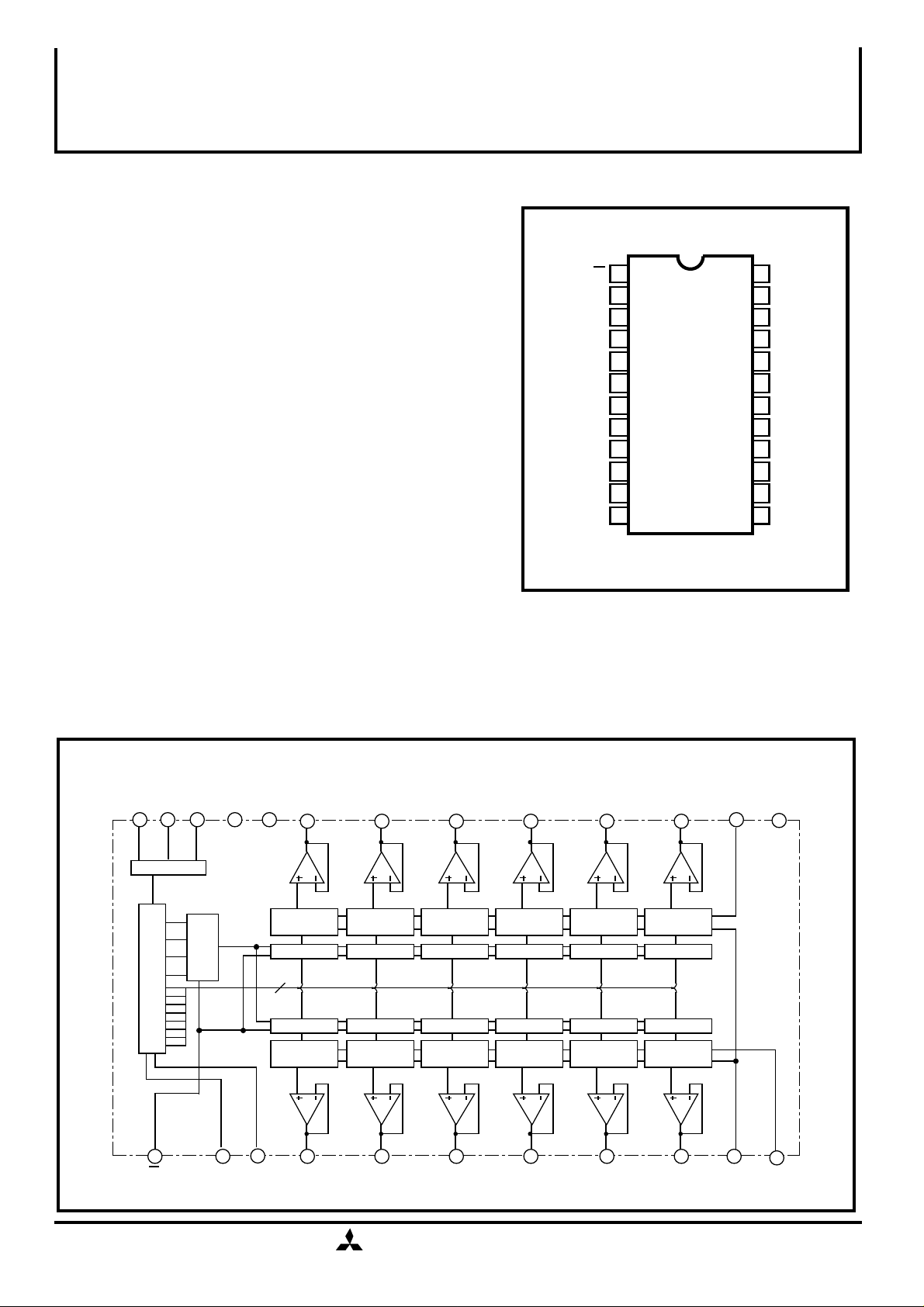
PIN CONFIGURATION (TOP VIEW)
R
SCL
SDA
Ao7
Ao8
Ao9
Ao10
Ao11
Ao12
VrefL
VrefU1
GND
1
2
3
M62392P,FP
4
5
6
7
8
9
10
11
12 13
Outline
24P4D(P)
24P2N-B(FP)
24
23
22
21
20
19
18
17
16
15
14
CS0
CS1
CS2
VDD
VCC
Ao6
Ao5
Ao4
Ao3
Ao2
Ao1
VrefU2
APPLICATION
Conversion from digital data to analog control data for both consumer and industrial equipment.
Gain control and automatic adjustment of DISPLAY-MONITOR or CTV.
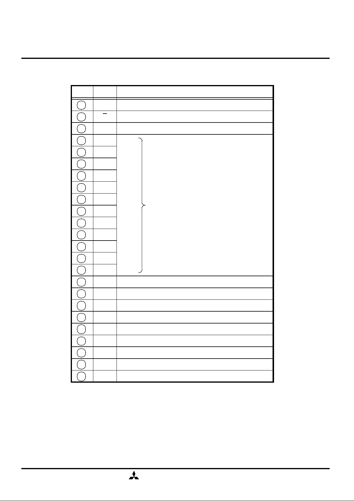
BLOCK DIAGRAM
Vcc
21222324
CHIP SELECT
ADDRESS
DECODER
I2C BUS TRANSCEIVER
20
8bit upper
segment R-2R
8bit Latch
8
8bit Latch
8bit upper
segment R-2R
19
18
8bit upper
segment R-2R
8bit Latch
8bit Latch
8bit upper
segment R-2R
8bit upper
segment R-2R
8bit Latch
8bit Latch
8bit upper
segment R-2R
1617
8bit upper
segment R-2R
8bit Latch
8bit Latch
8bit upper
segment R-2R
15
8bit upper
segment R-2R
8bit Latch
8bit Latch
8bit upper
segment R-2R
14
8bit upper
segment R-2R
8bit Latch
8bit Latch
8bit upper
segment R-2R
VrefU2Ao1Ao2Ao3Ao4Ao5Ao6VDDCS2CS1CS0
GND
12
13
1 4 5 6
R
2 3
SCL SDA VrefLAo7 Ao8 Ao9 Ao10
MITSUBISHI ELECTRIC
7
8 9
Ao11
Ao12
10
11
VrefU1
1997-5-27C.rev
( / 7 )
1
Page 2
8-BIT 12CH I2C BUS D-A CONVERTER WITH BUFFER AMPLIFIERS
EXPLANATION OF TERMINALS
MITSUBISHI <Dig./Ana. INTERFACE>
M62392P,FP
PIN No. Symbol
3
1
2
14
15
16
17
18
19
4
5
6
7
8
SDA
R
SCL
Ao1
Ao2
Ao3
Ao4
Ao5
Ao6
Ao7
Ao8
Ao9
Ao10
Ao11
F u n c t i o n
Serial data input terminal
Reset signal input terminal
Serial clock input terminal
8bit D–A converter output terminal
20
21
12
10
11
13
22
23
24
9
Ao12
VCC
VDD
GND
VrefL
VrefU1
VrefU2
CS2
CS1
CS0
Analog power supply terminal
Digital power supply terminal
Analog and digital common GND
D–A converter low level reference voltage input terminal
D–A converter high level reference voltage input terminal 1
D–A converter high level reference voltage input terminal 2
Chip select data input terminal 2
Chip select data input terminal 1
Chip select data input terminal 0
MITSUBISHI ELECTRIC
1997-5-27C.rev
( / 7 )
2
Page 3
ABSOLUTE MAXIMUM RATING
MITSUBISHI <Dig./Ana. INTERFACE>
M62392P,FP
8-BIT 12CH I2C BUS D-A CONVERTER WITH BUFFER AMPLIFIERS
Symbol
VCC
VDD
VrefU1,2
Vin
Vo
Pd
Topr
Tstg
Supply voltage
Supply voltage
D–A converter HIGH level
reference voltage
Input voltage
Output voltage
Power dissipation
Operating temperature
Storage temperature
Parameter Conditions
Ratings
–0.3 to 7.0
–0.3 to 7.0
–0.3 to 7.0
–0.3 to
–0.3 toVCC+0.3
465(DIP) / 421(FP)
+0.3
V
DD
–20 to 85
–55 to 125
Unit
V
V
V
V
V
mW
°C
°C
ELECTRICAL CHARACTERISTICS
<Digital part> (VCC,VDD,Vref U1,2=+5V±10%,VCC≥Vref U1,2,GND=VrefL=0V,Ta=–20 to 85°C unless otherwise noted)
Symbol
Supply voltage
IDD Supply current mA
Input leak current
IILK
Parameter
Test conditions
CLK=1MHz operation
IAO=0µA
VIN=0~VDD
MIN TYP MAX
–10
Ratings
4.5 5.0 5.5
1.0
10
Unit
VVDD
µA
Input low voltage 0.2VDD VVIL
Input high voltage 0.8VDD
VIH
<Analog part> (VCC,VDD,Vref U1,2=+5V±10%,VCC≥VrefU1,2,GND=VrefL=0V,Ta=–20 to 85°C unless otherwise noted)
Symbol Parameter
VCC Supply voltage
IrefU
VrefU
VrefL
SZERO
SFULL
D-A converter high level
reference voltage input current
D-A converter high level
reference voltage range
D-A converter low level
reference voltage range
Buffer amplifier output
VAO
voltage range
Buffer amplifier output
IAO
drive range
SDL
Differential nonlinearity
SL
Nonlinearity
Zero code error
Full scale error
Test conditions
CLK=1MHz operation IAO=0µAICC Supply current
VrefU=5V,VrefL=0V
Data condition:at maximum current
The output dose not necessarily
be the values within the
reference voltage setting range.
IAO=±100µA
IAO=±500µA
Upper side saturation voltage=0.3V
Lower side saturation voltage=0.2V
VrefU=4.79V
VrefL=0.95V
VCC=5.5V(15mV/LSB)
without load
(IAO=0)
MIN TYP MAX
GND
–1.0 1.0 mA
–1.0 1.0
–1.5 1.5
–2.0 2.0
–2.0 2.0
Ratings
4.5 5.0 5.5 V
1.0 3.0
1.4
3.5 VCC V
0.1 V
0.2
3.0
VCC-3.5
VCC-0.1
VCC-0.2
V
Unit
mA
mA
V
V
LSB
LSB
LSB
LSB
Co
Output capacitive load
Buffer amplifier
Ro
output impedance
MITSUBISHI ELECTRIC
5.0
0.1
1997-5-27C.rev
µF
Ω
( / 7 )
3
Page 4

I2C BUS LINE CHARACTERISTICS
MITSUBISHI <Dig./Ana. INTERFACE>
M62392P,FP
8-BIT 12CH I2C BUS D-A CONVERTER WITH BUFFER AMPLIFIERS
Symbol
fSCL
tBUF
tHD:STA
tLOW
tHIGH
tSU:STA
tHD:DAT
tSU:DAT
tR
tF
tSU:STO
Parameter
SCL clock frequency
Time the bus must be free before a new transmission can start
Hold time START Condition. After this period,the first clock
pulse is generated.
LOW period of the clock
HIGh period of the clock
Set-up time for START condition (Only relevant for a repeated
START condition)
Hold time DATA
Set-up time DATA
Rise time of both SDA and SCL lines
Fall time of both SDA and SCL lines
Set-up time for STOP condition
Normal mode
Min.
0
4.7
4.0
4.7
4.0
4.7
0
250
-
-
4.0
Max.
100
-
-
-
-
-
-
-
1000
300
-
High speed mode
Min.
0
1.3
0.6
1.3
0.6
4.7
0
100
20+
20+
0.6
Max.
400
-
-
-
-
-
0.9
-
300
300
-
units
KHz
µs
µs
µs
µs
µs
µs
ns
ns
ns
µs
*Note that a transmitter must internally provide at least a hold time to bridge the undefined
region (max.300 ns) of the falling edge of SCL.
TIMING CHART
tR, tF
tBUF
VIH
SDA
VIL
tSU:STA
tSU:STO
SCL
tHD:STA
tHD:DATtSU:DAT
VIH
VIL
tLOW
tHIGH
START START STOP START
MITSUBISHI ELECTRIC
1997-5-27C.rev
4
( / 7 )
Page 5

MITSUBISHI <Dig./Ana. INTERFACE>
M62392P,FP
8-BIT 12CH I2C BUS D-A CONVERTER WITH BUFFER AMPLIFIERS
I2C BUS FORMAT
STA SLAVE ADDRESS W A SUB ADDRESS A DAC DATA A STP
DIGITAL DATA FORMAT
•SLAVE ADDRESS
First
0 0
1
1
A2 A1 A0
CHIP SELECT DATA(SLAVE ADDRESS)
Last
•DAC DATA
First
MSB
Last
LSB
D2 D1 D0D3D4D5D6D7
(1)CHIP SELECT DATA
MSB LSB
A2 A1 A0
0
0 0 0 0 0
0 0 0 0 1
1 10 0
0 0
1 1 1 1
Lower 3bits(A0,A1,A2) are a programmable address. This
IC is accessed only when the lower 3 bits data of slave
address coincide with the data of CS0 to CS2.(refer to the
upper table)
CS2 CS1 CS0
1
11
•SUB ADDRESS
First
X X X S2 S1 S0S3X
Don't care
CHANNEL SELECT DATA
(2)CHANNEL SELECT DATA
MSB LSB
S3
0
0
0
1
1
1
1
S2
0
0
0
0
1
1
1
S1
0
0
1
1
0
0
1
S0
0
1
0
1
0
1
1
Channel selection
ch1 selection
ch2 selection
ch11 selection
ch12 selection
Last
Don't care.
Don't care.
Don't care.
(3)DAC DATA
First Last
MSB
LSB
D7 D6 D5 D4 D3 D2 D1 D0
0 0 0 0 0 0 0 0
0 0 0 0 0 0 0 1
0 0 0 0 0 0 1 0
0 0 0 0 0 0 1 1
1 1 1 1 1 1 1 0
1 1 1 1 1 1 1 1
MITSUBISHI ELECTRIC
DAC output
(VrefU-VrefL)/256 x 1+VrefL
(VrefU-VrefL)/256 x 2+VrefL
(VrefU-VrefL)/256 x 3+VrefL
(VrefU-VrefL)/256 x 4+VrefL
(VrefU-VrefL)/256 x 255+VrefL
VrefU
1997-5-27C.rev
( / 7 )
5
Page 6

TIMING CHART (MODEL)
•start condition to slave address bite
MITSUBISHI <Dig./Ana. INTERFACE>
M62392P,FP
8-BIT 12CH I2C BUS D-A CONVERTER WITH BUFFER AMPLIFIERS
SDA
1 2 A
SCL
R
DAC
output
start condition
•sub address bite
SDA
1 2
SCL
R
DAC
output
•DAC data bite to stop condition
3 4
3 4 5
5 6 7 W
6 7 8
A
SDA
1 2 A3 4 5 6 7 8
SCL
R
DAC
output
•Start condition ……… With SCL at HIGH,SDA line goes from HIGH to LOW
•Stop condition ……… With SCL at HIGH,SDA line goes from LOW to HIGH
(*Under normal circumstances,SDA is changed when SCL is LOW)
•Acknowledge bit …… The receiving IC has to pull down SDA line whenever receive slave data.
(The transmitting IC releases the SDA line just then transmit 8bit data.)
stop condition
MITSUBISHI ELECTRIC
1997-5-27C.rev
( / 7 )
6
Page 7

PRECAUTION FOR USE
M62392 have 5 terminals (VDD,VCC,VrefU1,VrefU2,VrefL) for input constant voltage at
use.
IF ripple or spike is input these terminals,accuracy of D-A conversion is down.
So,when use this device,please connect capacitor among each terminal to GND for
stable D-A conversion.
This IC's output amplifier has an advantage to capacitive load.So it's no problem at
device action when connect capacitor (0.1µF MAX) among output to GND for every
noise eliminate.
APPLICATION EXAMPLE
MITSUBISHI <Dig./Ana. INTERFACE>
M62392P,FP
8-BIT 12CH I2C BUS D-A CONVERTER WITH BUFFER AMPLIFIERS
5V
CHIP SELECT
DATA SETTING
RESET SIGNAL
5V
5V
5V
MCU
10µF
10µF
10µF
CS2
CS1
CS0
R
VrefU1
VrefU2
SCL
SDA
VDD VCC
GND VrefL
AO1
AO2
AO3
AO4
AO5
AO6
AO7
AO8
AO9
AO10
AO11
AO12
10µF
ch1
ch2
ch3
ch4
ch5
ch6
ch7
ch8
ch9
ch10
ch11
ch12
5V
ANALOG OUTPUT
TERMINALS
10µF
*Purchase of MITSUBISHI ELECTRIC CORPORATION'S I2C components conveys a license under the Philips I2C Patent Rights to
use these components an I2C system,provided that the system conforms to I2C Standard Specification as defined by Philips.
Mitsubishi Electric Corporation puts the maximum effort into making semiconductor products better and more reliable,
!
but there is always the possibility that trouble may occur with them. Trouble with semiconductors may lead to personal
injury,fire or property damage.Remember to give due consideration to safety when making your circuit design,in order to
prevent fires from spreading,redundancy,malfunction or other mishap.
MITSUBISHI ELECTRIC
1997-5-27C.rev
( / 7 )
7
 Loading...