

Page 1
MITSUBISHI<Dig.Ana.INTERFACE>
to use due to serial data input,and 3-pin(DI,CLK,LD)connection with
microcomputer.
The IC also contains Do pin terminal,enabling cascade
connection.The built-in buffer operational amplifiers are of full-swing
design with a wide operating supply voltage range for input/output
voltage.In addition,this IC provides improved stability against a
capacitive load,and therefore is suitable for application to electronic
volume(VCA)control,substitute for adjustment semi-fixed
resistor,etc.
operational amplifiers.
display.
D0D7123456D8
9
10
-
-
M62366GP
3V TYPE 8-BIT 12CH D-A CONVERTER WITH BUFFER AMPLIFIERS
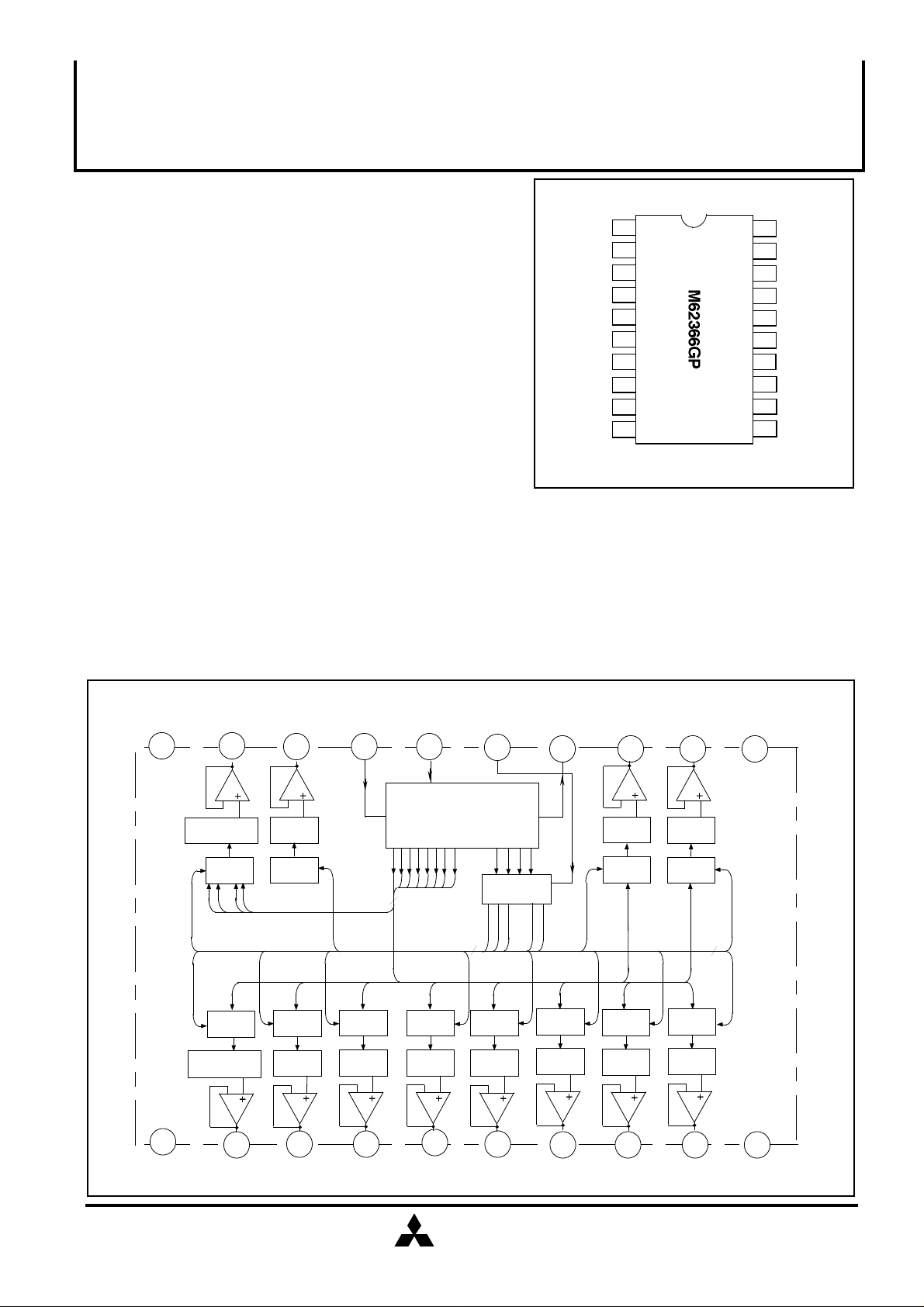
DESCRIPTION
The M62366GP is a CMOS semiconductor IC,containing 12
channels of 8-bit D-A converters,with a high-performance buffer
operational amplifier provided in the output of each channel. It is
operable with a low supply voltage between 2.7~3.6V,and is easy
FEATURES
•Operable with a low voltage between 2.7~3.6V
•12-bit serial data input(connected via 3 pins:DI,CLK,LD)
•12 channels of R-2R and segment type high-performance 8-bit
D-A converters
•12 buffer operational amplifiers with full swing of output voltage
between Vcc and GND.
•High oscillation stability against the capacitive load of buffer
APPLICATION
Adjustment/control of industrial or home-use electric
equipment,such as VTR camera,VTR set,TV,and CRT
PIN CONFIGURATION (TOP VIEW)
VSS
(VrefL)
Ao3
Ao4
Ao5
Ao6
Ao7
Ao8
Ao9
Ao10
VDD
(VrefU)
1
2
3
4
5
6
7
8
9
10
Outline 20P2E-A
20
GND
19
Ao2
18
Ao1
DI
17
16
CLK
15
LD
14
Do
Ao12
13
12
Ao11
Vcc
11
BLOCK DIAGRAM
GND
20 19
BUFFER
OPERATIONAL
AMPLIFIER
1
Vss
(VrefL)
Ao2
-
8-BIT
R-2R + SEGMENT
D-A CONVERTER
Ch2
8-BIT
LATCH
.....
(12)
8-BIT
LATCH
Ch3
8-BIT
R-2R + SEGMENT
D-A CONVERTER
-
2
Ao3
Ao1
DI
18 17 16
12-BIT SHIFT REGISTER
D-A
1
L
L
4
D-A
-
L
5
D-A
-
3 4
Ao4
Ao5
(8)
CLK
LD Do
15
D11
ADDRESS
DECODER
7
.....
L
8
D-A
(12)
L
6
D-A
-
5
6
Ao6 Ao7 Ao8
MITSUBISHI
ELECTRIC
Ao12 Ao11 Vcc
14 13 12
D-A
12 11
L
L
D-A
-
9
L
10
D-A
-
7 8 9
Ao9
-
D-A
L
L
D-A
-
Ao10
(12)
11
10
VDD
(VrefU)
( / 5 )
1
Page 2
3V TYPE 8-BIT 12CH D-A CONVERTER WITH BUFFER AMPLIFIERS
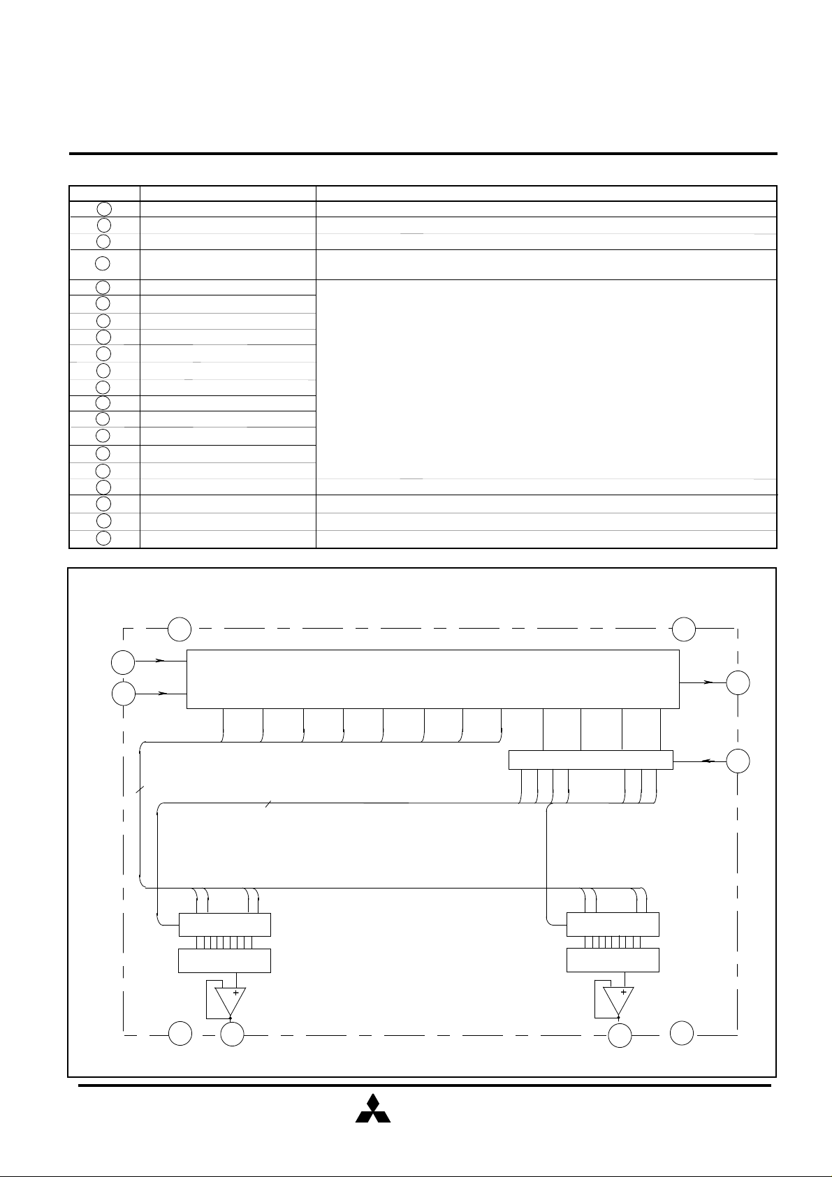
EXPLANATION OF TERMINALS
Pin No. Symbol
17
14
16
15
18
19
2
3
4
5
6
7
8
9
12
13
11
20
10
1
DI
Do
CLK
LD
Ao1
Ao2
Ao3
Ao4
Ao5
Ao6
Ao7
Ao8
Ao9
Ao10
Ao11
Ao12
VCC
GND
VDD
VSS
MITSUBISHI<Dig.Ana.INTERFACE>
M62366GP
Function
Serial data input terminal to input 12-bit long serial data
Terminal to output MSB data of 12-bit shift register
Shift clock input terminal.Input signal at DI pin is input to 12-bit shift register at rise of shift clock pulse
When H-level signal is input to this terminal,the value stored in 12-bit shift register is loaded
in decoder and D-A converter output register
8-bit D-A converter output terminal
Power supply terminal
GND terminal
D-A converter upper reference voltage input terminal
D-A converter lower reference voltage input terminal
BLOCK DIAGRAM FOR EXPLANATION OF TERMINALS
Vcc
11
DI
17
12-BIT SHIFT REGISTER
16
CLK
8
1
D0
8-BIT
R-2R + SEGMENT
D-A CONVERTER
D0
............
8-BIT
LATCH
-
D1
D2
12
D7
..............................................12
..............................................
...................................................................................................
D3
D4
D5
D6 D7
D8
D9
D10 D11
ADDRESS DECODER
...............
3
21
............
D0
8-BIT
LATCH
8-BIT
R-2R + SEGMENT
D-A CONVERTER
-
GND
20
1415Do
LD
124
D7
10
VDD
(VrefU)
18
Ao1
MITSUBISHI
ELECTRIC
13
Ao12
1
Vss
(VrefL)
( / 5 )
2
Page 3

DIGITAL DATA FORMAT
LAST
LSB
MITSUBISHI<Dig.Ana.INTERFACE>
M62366GP
3V TYPE 8-BIT 12CH D-A CONVERTER WITH BUFFER AMPLIFIERS
FIRST
MSB
DAC SELECT DATADAC DATA
D0
0
1
0
1
0
1
D8 D9 D10 D11
0
0
0
0
0
0
0
0
1
1
1
1
1
1
1
1
D1 D2 D3 D4
0
0
1
1
1
1 1 1 1 1 1 1
0
0
0
0
1
1
1
1
0
0
0
0
1
1
1
1
0
0
0
0
1
0
0
1
1
0
0
1
1
0
0
1
1
0
0
1
1
0
1
0
1
0
1
0
1
0
1
0
1
0
1
0
1
0
0
0
0
1
Don‘t care
Ao1 selection
Ao2
Ao3
Ao4
Ao5
Ao6
Ao7
Ao8
Ao9
Ao10
Ao11
Ao12
Don‘t care
Don‘t care
Don‘t care
0
0
0
0
1
DAC selection
D5
D6
0
0
0
0
1
0
0
0
0
1
D7
0
0
0
0
1
VrefU=VDD
*
VrefL=Vss
(VrefU-VrefL) / 256 X 1 +VrefL
(VrefU-VrefL) / 256 X 2 +VrefL
(VrefU-VrefL) / 256 X 3 +VrefL
(VrefU-VrefL) / 256 X 4 +VrefL
(VrefU-VrefL) / 256 X 255 +VrefL
VrefU
D-A output
TIMING CHART (MODEL)
DI
CLK
LD
D-A
OUTPUT
MSB
D11 D10
D9
D8 D0D1
MITSUBISHI
ELECTRIC
D2
LSB
( / 5 )
3
Page 4

MITSUBISHI<Dig.Ana.INTERFACE>
M62366GP
3V TYPE 8-BIT 12CH D-A CONVERTER WITH BUFFER AMPLIFIERS
ABSOLUTE MAXIMUM RATINGS
Symbol Ratings
Vcc
VDD
VIN
Vo
Pd
Topr
Tstg Storage tempareture
Supply voltage
Upper reference voltage of D-A converter
Input voltage
Output voltage
Power dissipation
Operating temperature
Parameter
ELECTRICAL CHARACTERISTICS
Digital part(VCC,VrefU=+3V±10%, VCC≥VrefU,GND,VrefL=0V,Ta=-20 ~ +85°C,unless otherwise noted)
Symbol
VCC
Icc
IILK
VIL
VIH
VOL
VOH
Note:The standard values are obtaind at Ta=25°C
Supply voltage
Circuit current
Input leak current
Input low voltage
Input high voltage
Output low voltage
Output high voltage
Parameter
CLK=1MHz operation,Vcc=3V,IAO=0µA
VIN=0~VCC
IOL=2.5mA
IOH=-400µA
Conditions
Test conditions
-0.3~+7.0
-0.3~+7.0
-0.3~VCC+0.3
-0.3~VCC+0.3
-20~+85
-55~+150
Min.
2.7
-10
0.8VCC
VCC-0.4
150
Limits
Typ.
3.0
Max.
3.6
3.5
10
0.2VCC
0.4
Unit
V
V
V
V
mW
°C
°C
Unit
V
mA
µA
V
V
V
V
Analog part(VCC,VrefU=+3V±10%, VCC≥VrefU,Ta=-20 ~ +85°C,unless otherwise noted)
Symbol
IrefU Current dissipation
VrefU
VrefL
VAO
IAO
SDL
SL
SZERO
SFULL
Co
Ro
D-A converter upper reference
voltage range
D-A converter lower reference
voltage range
Buffer amplifier output driver voltage
range
Buffer amplifier output voltage
range
Differential nonlinearity error
Nonlinearity error
Zero code error
Full scale error
Output capacitative load
Buffer amplifier output impedance
Parameter
VrefU=3V,VrefL=0V
Data condition:maximum current
Reference voltage can not always be set to
any value in this range,because it is restricted
to the buffer amplifier output voltage range
IAO=±100µA
IAO=+500µA
-200µA
Upper saturation voltage=0.4V
Lower saturation voltage=0.4V
Vcc=2.760V
VrefU=2.610V
VrefL=0.050V(10mV/LSB)
Without load(IAO=±0)
Test conditions
Min.
0.7Vcc
GND
0.1
0.2
-0.3
-1.0
-1.5
-2
-2
Limits
Typ.
1.4
5
Max.
2.5
Vcc
0.3Vcc
Vcc-0.1
Vcc-0.2
1
1.0
1.5
2
2
0.1
Unit
mA
V
V
V
mA
LSB
LSB
LSB
LSB
µF
Ω
MITSUBISHI
ELECTRIC
( / 5 )
4
Page 5

MITSUBISHI<Dig.Ana.INTERFACE>
M62366GP
3V TYPE 8-BIT 12CH D-A CONVERTER WITH BUFFER AMPLIFIERS
AC CHARACTERISTICS(VCC,VrefU=+5V±10%, VCC≥VrefU,GND,VrefL=0V,Ta=-20 ~ +85°C,unless otherwise noted)
Symbol
tCKL
tCKH
tCR
tCF
tDCH
tCHD
tCHL
tLDC
tLDH
tDo
tLDD
Parameter
Clock "L"pulse width
Clock "H"pulse width
Clock rise time
Clock fall time
Data set up time
Data hold time
LD set up time
LD hold time
LD "H" pulse duration
Data output delay time
D-A output setting time
Test conditions
CL=100pF
CL≥100pF,VAO:0.1 2.6V
The time until the output becomes
the final value of 1/2 LSB
Min Typ
200
200
30
60
200
100
100
70 350
Limits
Max
200
200
300
Unit
ns
ns
ns
ns
ns
ns
ns
ns
ns
ns
µs
TIMING CHART
CLK
DI
LD
D-A
OUTPUT
Do
OUTPUT
tCR tCF
tCKL
tDCH
tCKH
tCHD
tDo
tLDC
tLDH
tCHL
tLDD
MITSUBISHI
ELECTRIC
( / 5 )
5
 Loading...