

Page 1
MITSUBISHI<Dig.Ana.INTERFACE>
output(0 scale)when power is turned ON or drops.
COMPARATOR
M62361FP
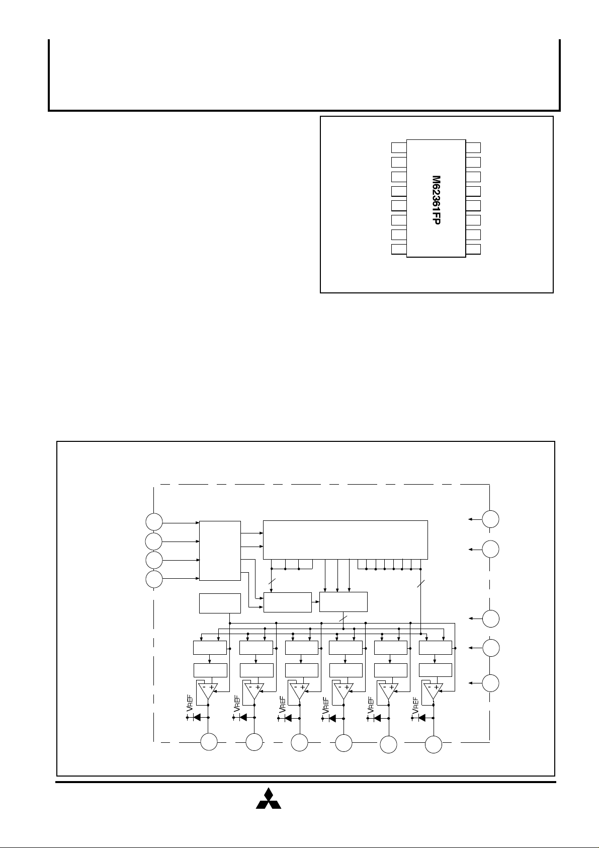
8-BIT 6CH D-A CONVERTER WITH BUFFER AMPLIFIERS
DESCRIPTION
The M62361FP is a Bi-CMOS semiconductor IC,containing 6
channels of 8-bit D-A converters(DAC),with a buffer operational
amplifier provided in the output of each channel.It is easy to use
due to serial data input, and three-pin(DT,CK,ST)connection with
microcomputer.
This IC is designed to be operable when chip select data
contained in the 15-bit data conforms to the state of the CS
terminal.Accordingly,the IC can process data by strobe signals
common with other devices connected to the bus of
microcomputer, and does not involve an microcomputer port to
drive the IC.The inputs are connected to a level shift circuit so
that the input threshold level does not depend on supply
voltage.The IC also contains an initialization function to reset
FEATURES
•Output buffer operational amplifier provided in each channel
•15-bit serial data input
•6 channels of R-2R and segment type 8-bit DAC
•Chip select terminal
•Power-on reset function
APPLICATION
Digital-analog conversion in industrial or home-use electric
equipment.
Automatic control in combination with EEROM and
microcomputer(Substitute for conventional semi-fixed
resistor)
Signal gain setting of display monitor and CTV.
PIN CONFIGURATION (TOP VIEW)
DK
CK
ST
CS
NC
D.G
A.G
Vss
1
2
3
4
Outline 16P2N-A
16
VDD
15
Ao1
14
Ao2
13
Ao3
125
Ao4
Ao5
116
Ao6
107
98
VREF
NC:NO CONNECTION
BLOCK DIAGRAM
DT
CK
ST
CS
VDD
1
2
3
4
LEVEL
SHIFT
RESET
CIRCUIT
8-BIT
LATCH
8-BIT DAC
15
Ao1
15 14 13 12 11 10 9 8 7 6 5 4 3 2 1
8-BIT
LATCH
8-BIT DAC
14
Ao2
15-BIT SHIFT RESISTER
4
DECODER
8-BIT
LATCH
8-BIT DAC
13
Ao3
8-BIT
LATCH
8-BIT DAC
12
Ao4
8
6
8-BIT
LATCH
8-BIT DAC
11
Ao5
8-BIT
LATCH
8-BIT DAC
10
Ao6
16
6
D.G
9
VREF
VSS
8
7
A.G
MITSUBISHI
ELECTRIC
( / 8 )
1
Page 2
EXPLANATION OF TERMINALS
Pin No. Symbol
1
2
3
4
16
6
7
9
8
15
14
13
12
11
10
5
DT
CK
ST
CS
VDD
D•G
A•G
VREF
Vss
Ao1
Ao2
Ao3
Ao4
Ao5
Ao6
NC
MITSUBISHI<Dig.Ana.INTERFACE>
M62361FP
8-BIT 6CH D-A CONVERTER WITH BUFFER AMPLIFIERS
Function
Serial data input terminal
Shift clock input terminal to input data at rise of clock pulse
Strobe input terminal to latch data in the register when H-level signal is input
Chip select terminal
Power supply terminal for input level shift circuit and buffer amplifier
GND terminal for digital line
GND terminal for analog line
8-bit D-A converter power supply terminal
8-bit D-A converter minimum power supply terminal
8-bit D-A converter output terminal
Not used
TIMING CHART (MODEL)
DT
CK
ST
AO
LSB
D01 D02
D03
D04
D02
D03
D04
MITSUBISHI
ELECTRIC
( / 8 )
2
Page 3
MITSUBISHI<Dig.Ana.INTERFACE>
M62361FP
8-BIT 6CH D-A CONVERTER WITH BUFFER AMPLIFIERS
ABSOLUTE MAXIMUM RATINGS(Ta=25°C, unless otherwise noted)
Symbol Ratings
VDD
VREF
VIN
Ao
Pd
K
Topr
Tstg
Supply voltage
Reference voltage
Input voltage
Output voltage
Power dissipation
Thermal derating
Operating temperature
Storage temperature
Parameter
ELECTRICAL CHARACTERISTICS
DC CHARACTERISTICS( Ta=25°C,VDD=8.0V,VREF=5.0V,Vss=0V,RL=2kΩ unless otherwise noted)
Symbol
VDD
IDD
VREF
Vss
IREF
RSL
EZR
EFS
DNL
ECH
VIH
VIL
IIH
IIL
VAO
Isink
Current dissipation
Voltage range at VREF
Voltage range at Vss
Maximum sink current at VREF
Resolution
Zero point error
Full scale error
Differential nonlinearity error
Error between channels
Input voltage
Input current
Output voltage range
Output sink current
H-level
L-level
H-level
L-level
Ta=-25 ~ +85°C
Set at
VREF=VDD-2V
Set at
Vss≥0.3V
Monotony assured
VDD=6.0 ~ 10V
VDD=6.0 ~ 10V
VDD=6.0 ~ 10V
VDD=6.0 ~ 10V
Set at
Conditions
Test conditions
128
for all channels. RL=∞
256
107
for all channels.
256
15
min. for all channels.
256
-0.3~+15
-0.3~+8
-0.3~VDD
-0.3~VDD
-20~+85
-55~+125
Min.
6.0 8.0 14.0
4.0
-0.2
-1.5
-1.5
-1.0
-3
3.5
0
0.3
0
550
5.5
Limits
Typ.
5 10
0.0
1.5
0
-1.5
Max.
7.5
1.0
3
8
1.5
1.5
1
3
VDD
1.0
10
10
VREF
-2LSB
100
Unit
V
V
V
V
mW
mW/°C
°C
°C
Unit Parameter
VOperating supply voltage
mA
V
V
mA
bit
LSB
LSB
LSB
LSB
V
V
µA
µA
V
µA
Isource
SR
VS1
∆VS1
VS2
∆VS2
(*Full scale range = maximum output voltage setting)
Output source current
Output through rate
Reset detection voltage 1
Hysteresis voltage 1
Reset detection voltage 2
Hysteresis voltage 2
For FSR*,Ao≥FSR-2LSB
Detection of VDD power
Detection of VDD power
Detection of VREF power
Detection of VREF power
MITSUBISHI
ELECTRIC
-5
0.3
4.25
0.05
2.85
0.03
4.45
0.1
3.0
0.06
0
4.65
0.2
3.15
0.15
( / 8 )
3
mA
V/µs
V
V
V
V
Page 4

MITSUBISHI<Dig.Ana.INTERFACE>
M62361FP
8-BIT 6CH D-A CONVERTER WITH BUFFER AMPLIFIERS
AC CHARACTERISTICS( Ta=25°C,VDD=8.0V,VREF=5.0V,Vss=0V,RL=2kΩ unless otherwise noted)
Symbol
tCKL
tCKH
tCR Clock rise time
tCF
tDCH
tCHD
tCHS
tSTC
tSTH
tSTD
Clock "L"pulse width
Clock "H"pulse width
Clock fall time
Data set up time
Data hold time
ST set up time
ST hold time
ST "H" pulse width
Ao output setting time
Parameter
0 FSR FSR 0
Test conditions
Min Typ
200
200
300
200
500
500
500
Limits
Max
200
200
20
Unit
ns
ns
ns
ns
ns
ns
ns
ns
ns
µs
TIMING CHART
CK
DT
ST
Ao
tCR tCF
tCKL
tDCH
tCKH
tCHD
tSTC
tSTH
tCHS
tSTD
MITSUBISHI
ELECTRIC
( / 8 )
4
Page 5

8-BIT 6CH D-A CONVERTER WITH BUFFER AMPLIFIERS
01234
DESCRIPTION OF OPERATION
1.Level shift circuit
The logical operation in the IC is controlled by VREF voltage.
Therefore,the logical level of input is shifted to DG(Low)or
VREF(High),regardless of fluctuating VDD.
2.15-bit shift register
Data necessary for setting DAC is serially input.The data is
input at positive edge of CK signal.The register is capable of
retaining 15-bit data consisting of 3 blocks:DAC data.DAC
select data and chip select data.
(1)15 bit serial data
(LSB)
1
DATA
CK
(2)Data allocation
(LSB)
2
(MSB)
8
9
10
11 12 13
(MSB)
:DAC SETTING DATA
14
MITSUBISHI<Dig.Ana.INTERFACE>
M62361FP
3.Decoder(DAC select decoder)
Appropriate one of the 6 DAC channels is selected by the 3bit DAC select data:S01,S02,S03.
S01
15
S02
0
1
0
1
0
1
0
1
S03
0
0
1
1
0
0
1
1
0
0
0
0
1
1
1
1
4.Comparator(Chip select data)
Whether DAC data is effective or not is determined by the
4-bit data(C01 ~ C04)and the logic at CS terminal.Either of
the following data combination is required.
C01
0
0
C02
0 1
0
C03
1
C04
1
0
VOUT
1
2
3
4
5
6
not select
not select
CS
0
1
:DAC SELECT DATA
:CHIP SELECT DATA
6.8-bit DAC + buffer amplifier
Potential difference between VREF and Vss is output with 8bit resolution,using the R-2R system.No resolution is obtained
for bit data lower than the output saturated voltage of the
buffer amplifiers data lower than the output saturated voltage
of the buffer amplifiers of analog output A01 to A06.The
minimum value of 300mA,given for the electrical
2 X D01 + 2 X D02 + 2 X D03 + 2 X D04 + 2 X D05 + 2 X D06 + 2 X D07 + 2 X D08
Ao=
256
5.8-bit latch circuit
When the data input to shift register meets the above
requirement for comparator,D01~D08 data are latched in the
channel selected by decoder.This data latching takes place
when input at ST terminal is HIGH.
characteristic concerning output voltage
range(VAO),indicates that no resolution is secured for
output lower than 300mV.
For all bit data,resolution is secured when Vss is operated
with 300mV or higher voltage.
5
6
7
• (VREF - Vss) + Vss
MITSUBISHI
ELECTRIC
( / 8 )
5
Page 6

DAC SETTING DATA(VREF=5.0V,Vss=0V)
(LSB)
MITSUBISHI<Dig.Ana.INTERFACE>
M62361FP
8-BIT 6CH D-A CONVERTER WITH BUFFER AMPLIFIERS
(MSB)
C01 C02 C03 C04 C05
0 0
0
0
1
1
0
0
0
1
0
1
0
1
1
0
0
0
0
1
1
1
1
1
1
C06 C07 C08
0
1
1
0
0
0
0
1
1
1
1
7.Reset circuit
This circuit monitors VDD and VREF,ensuring
stable analog output when power is turned ON or
OFF.If either input is abnormal,the reset circuit
causes output buffer amplifiers to stop operation
to retain the output in Vsat state,as well as
resetting DAC data(0 scale)of all channels.
RESET TIMING CHART
4.45
VDD
A01~A06
0
0
1
1
0
0
0
0
1
1
1
1
Vsat
VREF
VREF
VREF
VREF
X
X
X
X
If VREF drops earlier than VDD,the analog output
reset operation starts at point A.
4.5 DETECTED
(HYSTERESIS
VOLTAGE:100mV)
0
(15/256)
(16/256)
(17/256)
(254/256)
(255/256)
VREF
AO
3.06
(3.0V)
A
ALLOWABLE RANGE FOR SETTING OUTPUT
MITSUBISHI
ELECTRIC
3.0 DETECTED
(HYSTERESIS VOLTAGE:60mV)
t
( / 8 )
6
Page 7

APPLICATION EXAMPLE
MITSUBISHI<Dig.Ana.INTERFACE>
M62361FP
8-BIT 6CH D-A CONVERTER WITH BUFFER AMPLIFIERS
VREF=
7.5V max
MICRO
COMPUTER
REGULATOR
VDD=14V max
9
VREF
1
DT
2
CK
ST
3
CS
4
16
VDD
Ao1
Ao2
Ao3
Ao4
Ao5
Ao6
10
15
14
13
12
11
ch1
ch2
ch3
ch4
ch5
ch6
D.G
A.G
Vss
76
8
Vss=0.3~1.0V
When 8 pin is GND,Ao output is 0.3~VREF-1 LSB
When 8 pin is Vss,Ao output is Vss~VREF-1 LSB
MITSUBISHI
ELECTRIC
( / 8 )
7
Page 8

MITSUBISHI<Dig.Ana.INTERFACE>
8-BIT 6CH D-A CONVERTER WITH BUFFER AMPLIFIERS
TYPICAL CHARACTERISTICS(Ta=25°C,VDD=8.0V,VREF=5.0V,RL=2kΩ,unless otherwise noted)
M62361FP
CURRENT DISSIPATION VS.
AMBIENT TEMPERATURE
8
7
6
5
4
3
2
-20 0 20 40 60 80 100
AMBIENT TEMPERATURE Ta(°C)
RESET DETECTION VOLTAGE 1 VS.
AMBIENT TEMPERATURE
4.6
4.5
VREF SINK CURRENT VS.
AMBIENT TEMPERATURE
1.8
1.7
1.6
1.5
1.4
1.3
1.2
-20 0 20 40 60 80 100
AMBIENT TEMPERATURE Ta(°C)
RESET DETECTION VOLTAGE 2 VS.
AMBIENT TEMPERATURE
3.1
4.4
4.3
-20 0 20 40 60 80 100
AMBIENT TEMPERATURE Ta(°C)
NONLINEARITY ERROR
0.50
0.40
0.30
0.20
0.10
-0.00
-0.10
-0.20
-0.30
-0.40
-0.50
0 40 80 120 160 200
DATA
240
280
3.0
2.9
-20 0 20 40 60 80 100
AMBIENT TEMPERATURE Ta(°C)
DIFFERENTIAL NONLINEARITY ERROR
0.50
0.40
0.30
0.20
0.10
-0.00
-0.10
-0.20
-0.30
-0.40
-0.50
0 40 80 120 160 200
DATA
240
280
MITSUBISHI
ELECTRIC
( / 8 )
8
 Loading...