

Page 1
MITSUBISHI<Dig.Ana.INTERFACE>
mode to backup mode and vice versa. these output signals are
classified into pulse type(M62001~M62004) and hold type
(M62005~M62008).
equipment,and home-use electronic appliances.
M62001L,FP/M62002L,FP/M62003L,FP/M62004L,FP/
M62005L,FP/M62006L,FP/M62007L,FP/M62008L,FP
LOW POWER 2 OUTPUT SYSTEM RESET IC SERIES
DESCRIPTION
The M62001~8 are semiconductor integrated circuits whose
optimum use is for the detection of the rise and fall in the
power supply to a microcomputer system in order to reset or
release the microcomputer system.
The M62001~8 carry out voltage detection in 2 steps and
have 2 output pins.As Bi-CMOS process and low power
dissipating circuits are employed,they output optimum signals
through each output pin to a system that requires RAM
backup, As output signals,interruption(INT) and compulsive
reset(RESET) signals are available.The interruption
signal(INT) is used to alter the microcomputer from normal
FEATURES
•
Bi-CMOS process realizes a configuration of low current
dissipating circuits.
Circuit current
Icc=5µA(Typ.,normal mode,Vcc=5.0V)
Icc=1µA(Typ.,backup mode,Vcc=2.5V)
•Two-step detection of supply voltage
Detection voltage in normal mode (2 types)
Vs=4.45V/4.25V(Typ.)
Detection voltage in backup mode
VBATT=2.15V(Typ.)
•Two outputs
Reset output (RESET):Output of compulsive reset signal
Interruption output(INT):Output of interruption signal
•Two types of output forms:CMOS and open drain
•Two types of interruption output (INT) signals
Pulse type (M62001~M62004)
Hold type (M62005~M62008)
•Two types of outline packages
5-pin plastic SIP (single in-line package)
8-pin plastic SOP (mini flat package)
•Output based on RAM backup mode (See the timing chart.)
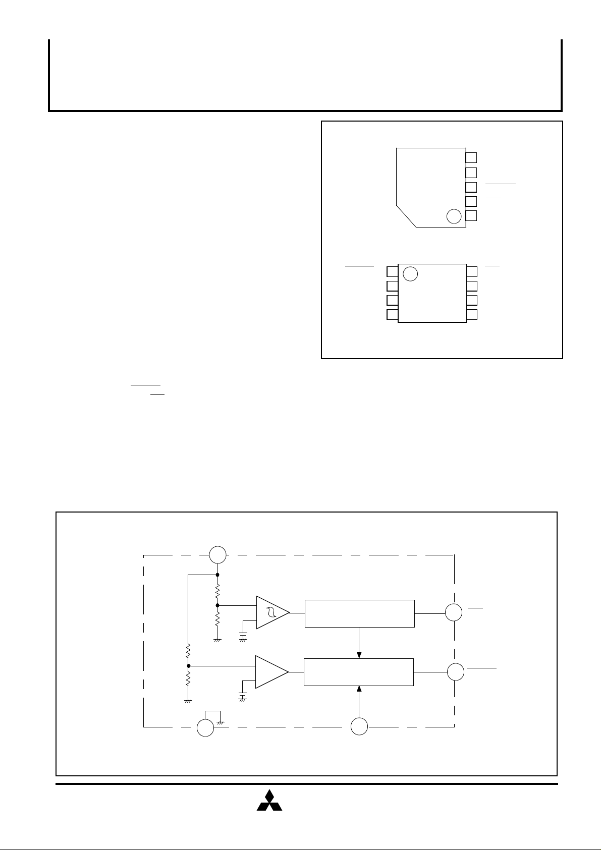
PIN CONFIGURATION (TOP VIEW)
5
Vcc
4
Cd
3
RESET
M62001L
Outline 5P5T(M62001L~8L)
RESET
Vcc
NC
1
2
Cd
3
4
Outline 8P2S-A(M62001FP~8FP)
M62001FP
2
INT
1
GND
8
INT
7
GND
6
NC
5
NC
NC:NO CONNECTION
APPLICATION
Prevention of malfunction of microcomputer systems in
electronic,equipment such as OA equipment, industrial
BLOCK DIAGRAM
Vcc
5
+
-
+
-
1
GND(GROUND PIN)
NOTE:This is an example showing pin Nos.of M62001L~8L.(See PIN CONFIGURATION.)
INTERRUPTION SIGNAL
GENERATION BLOCK
RESET SIGNAL
GENERATION BLOCK
4
Cd(PIN TO DELAY CAPACITANCE)
MITSUBISHI
ELECTRIC
2
3
INT
RESET
1
( / 6 )
Page 2
MITSUBISHI<Dig.Ana.INTERFACE>
Pulse output
Hold output
M62001L,FP/M62002L,FP/M62003L,FP/M62004L,FP/
M62005L,FP/M62006L,FP/M62007L,FP/M62008L,FP
LOW POWER 2 OUTPUT SYSTEM RESET IC SERIES
ABSOLUTE MAXIMUM RATINGS
(Ta=25°C, unless otherwise noted,These ratings commonly apply to the M62001L/FP~M62008L/FP.)
Symbol Ratings
Vcc
ISINK
Pd
K
Topr
Tstg Storage temperature
Supply voltage
Output sink current
Power dissipation
Thermal derating
Operating temperature
Parameter
(Ta≥25°C)
ELECTRICAL CHARACTERISTICS
(Ta=25°C, unless otherwise noted,These ratings commonly apply to the M62001L/8L.)
Symbol
Vs
VBATT Battery voltage
∆Vs
ICC
Vsat1
Vsat2
td
tpw
tRESET
tINT
Supply voltage
Hysteresis voltage
Circuit current
Sink ability
Source ability
Delay time
Pulse width
Reset output response time
Interruption output reset time
Parameter
Interruption level
during Vcc drop
(Equivalent to VSL)
Reset level at backup
∆Vs=VSH-VSL
Vcc=5.0V:In normal mode
Vcc=2.5V:In backup mode
Vcc=4V,Io=4mA
(Output saturation voltage of N-ch transistor)
Vcc=4V,Io=1mA
(Output saturation voltage of P-ch transistor:
[CMOS output] M62001,M62003,
M62005,M62007)
External capacitance Cd=0.33µF
Output pulse width (M62001,M62002,
M62003,M62004)
Time between Vcc(when falling)=VBATT and
output of RESET signal
Time between Vcc(when falling)=VS and
output of INT signal
Conditions
Test conditions
(M62001,M62002,
M62005,M62006)
(M62003,M62004,
M62007,M62008)
440
-20 ~ +75
-40 ~ +125
Limits
Min.
4.30
4.05
2.00
8
5
4.4
Typ.
4.45
4.25
2.15 2.30
5.0 20
1.0
0.2
100
Max.
4.60
4.45
50
7
30
4
0.4
0.40.2
10
Unit
V
mA
mW
mW/°C
°C
°C
Unit
V
V
mV100
µA
V
V
ms
µS
µS
µS
SUMMARY OF M62001L/FP~M62008L/FP
Type Output form
M62001
M62002
M62003
M62004
M62005
M62006
M62007
M62008
Supply voltage detection level Vs(V)
4.45
4.25
4.45
4.25
Battery voltage detection level VBATT(V)
2.15
Open drain
Open drain
Open drain
Open drain
MITSUBISHI
ELECTRIC
CMOS
CMOS
CMOS
CMOS
Interruption signal output mode
2
( / 6 )
Page 3

M62001L,FP/M62002L,FP/M62003L,FP/M62004L,FP/
VBATT
VSH
VSH
VSL
M62005L,FP/M62006L,FP/M62007L,FP/M62008L,FP
TYPICAL CHARACTERISTICS
MITSUBISHI<Dig.Ana.INTERFACE>
LOW POWER 2 OUTPUT SYSTEM RESET IC SERIES
CIRCUIT CURRENT vs.
SUPPLY VOLTAGE
10
8
6
4
2
0
0 2
SUPPLY VOLTAGE Vcc(V)
RESET OUTPUT VOLTAGE vs.
5
4
3
4 6 8 10
SUPPLY VOLTAGE
THERMAL DERATING
(MAXIMUM RATING)
1000
800
600
400
200
0
0
25
50
75
AMBIENT TEMPERATURE Ta(°C)
INTERRUPTION OUTPUT VOLTAGE vs.
5
4
3
SUPPLY VOLTAGE
100
125
2
1
0
0 1
SUPPLY VOLTAGE Vcc(V)
DELAY CAPACITANCE vs. DELAY TIME
10
1.0
0.1
0.01
1
2 3 4 5
10 100
DELAY TIME td(msec)
1000
2.0
1.5
1.0
0.5
2
1
0
0
1 2
SUPPLY VOLTAGE Vcc(V)
LIMIT OPERATING VOLTAGE
(OPEN DRAIN TYPE)
0
0
0.5 1.0
SUPPLY VOLTAGE Vcc(V)
3 4
RL=10kΩ
RL=100kΩ
RL=1MΩ
1.5
5
2.0
MITSUBISHI
ELECTRIC
( / 6 )
3
Page 4

MITSUBISHI<Dig.Ana.INTERFACE>
4
V
RES
V
INT
M62001L,FP/M62002L,FP/M62003L,FP/M62004L,FP/
M62005L,FP/M62006L,FP/M62007L,FP/M62008L,FP
LOW POWER 2 OUTPUT SYSTEM RESET IC SERIES
4.50
4.45
CIRCUIT CURRENT vs.
AMBIENT TEMPERATURE
7
6
5
4
3
2
Vcc=3V
1
0
-40
0
-20
AMBIENT TEMPERATURE Ta(°C)
DETECTION VOLTAGE vs.
AMBIENT TEMPERATURE
(DETECTION AT 4.45V TYPE)
20
Vcc=2V
40 60
Vcc=5V
80 100
DETECTION VOLTAGE vs.
AMBIENT TEMPERATURE
2.20
2.15
2.10
2.05
-40
-20
AMBIENT TEMPERATURE Ta(°C)
INTERRUPTION OUTPUT VOLTAGE vs.
20 40 60
0
SUPPLY VOLTAGE
5
4
3
80 100
4.40
4.35
-40
-20
AMBIENT TEMPERATURE Ta(°C)
Nch OUTPUT SATURATION VOLTAGE vs.
OUTPUT SINK CURRENT
20 40 60
0
80 100
0.5
Vcc
Vcc=4V
0.4
0.3
GND
Isink
Vsat
0.2
0.1
0
0
1
OUTPUT SINK CURRENT Isink(mA)
3 4
2
2
1
0
0
1 2
SUPPLY VOLTAGE Vcc(V)
Pch OUTPUT SATURATION VOLTAGE vs.
OUTPUT SOURCE CURRENT
3 4
5
0.5
Vcc=5 4V
0.4
0.3
Vcc
RES
GND
Vsat
Isource
0.2
0.1
0
0
5
OUTPUT SOURCE CURRENT Isource(mA)
1 2
3 4
5
MITSUBISHI
ELECTRIC
( / 6 )
Page 5

MITSUBISHI<Dig.Ana.INTERFACE>
In general,the memory backup function of
a microcomputer,as shown in figure,uses two diodes to switch
between main power supply and backup power supply.The
M62001~M62008 are ICs that,in such memory backup
operation,monitor in 2 steps each voltage on the VDD line.
hysteresis action of RESET toward normal state at restoration of
supply voltage,as well as 2-step detection in low power
dissipation mode.
output pins (INT and RESET).Although they have 2 comparators
for 2-step detection,they differ significantly from such that are
simply provided with independent detectors,because the RESET
output signal is dependent at power-up and the like upon the
INT output signal.
5
M62001L,FP/M62002L,FP/M62003L,FP/M62004L,FP/
M62005L,FP/M62006L,FP/M62007L,FP/M62008L,FP
LOW POWER 2 OUTPUT SYSTEM RESET IC SERIES
OPERATION PRINCIPLE
DESCRIPTION
Vcc
MAIN POWER
SUPPLY BACKUP
POWER
SUPPLY
The ICs have an intelligent sequence such as substantial
INT
RESET
M62001
VDD
INT
RESET
MICROCOMPUTER
SYSTEM
OPERATION IN DETAIL
1.Two Step Detection
The ICs perform 2-step detection of supply voltage and have 2
3.RESET Output (Detection of 2.15V)
The RESET outputs a signal to prevent the microcomputer from
malfunctioning due to a drop in supply voltage.
When powering up,RESET is kept at low level until the supply
voltage reaches VSH.If the supply voltage rises to VSH,RESET
is set to high level.By inserting a capacitor between the Cd pin
and GND,it is possible to produce a desired delay time (td).To
set a delay time,equation below is used.
Once the supply voltage has exceeded VSH and the RESET
output is set to high level,RESET maintains the high level until
the supply voltage drops to VBATT.When the supply voltage
drops to VBATT,RESET goes low thereby resetting and
initializing the microcomputer.
The RESET output has a large hysteresis voltage of
approximately 2V between the rise in supply voltage at powerup and its fall.
.
td=1.52X10 XCd(sec)
.
RESET OUTPUT VOLTAGE VS.
SUPPLY VOLTAGE
5
4
3
2.INT output (Detection of 4.45V and 4.25V)
The INT output at the power-up of supply voltage detects VSH
(4.45V/4.25V)to inform the microcomputer system of the fact
that the supply voltage has reached its normal level.When the
supply voltage drops from its normal level to
VSL(4.45V/4.25V)an interruption signal is output to alter the
microcomputer system into RAM backup mode. The
microcomputer at this point enters sleep state and secures
memory by a stop command issued by the interruption
signal.These detection voltage ,VSH the rise,and VSL the fall,of
supply voltage,have a 100-mV hysteresis voltage between
themselves.
VSH-VSL=100(mV)
INT OUTPUT VOLTAGE VS.
.
.
SUPPLY VOLTAGE
5
4
3
VSL VSH
2
2
1
0
VBATT
2
3
SUPPLY VOLTAGE Vcc
VSH
4
5
1
0
4.2 4.4 4.6
4.0
SUPPLY VOLTAGE Vcc(V)
4.8 5.0
MITSUBISHI
ELECTRIC
( / 6 )
5
Page 6

M62001L,FP/M62002L,FP/M62003L,FP/M62004L,FP/
,the INT output is set to high level.
(2.15V),the RESET
output is set to low thereby resetting the microcomputer
and initializing system.
7 Same as 1 .
8 Same as 2 .
9 Same as 3 and 5 .
7
M62005L,FP/M62006L,FP/M62007L,FP/M62008L,FP
OPERATION DESCRIPTION
MITSUBISHI<Dig.Ana.INTERFACE>
LOW POWER 2 OUTPUT SYSTEM RESET IC SERIES
VSH
VSL
Vcc
GND
INT
(HOLD OUTPUT TYPE)
GND
INT
(PULSE OUTPUT TYPE)
GND
RESET
GND
VSH
1
2
PULSE WIDTH
7µsec
td
VSL
3
VSH
td
VSL VBATT
UNCERTAIN AREA
UNCERTAIN AREA
UNCERTAIN AREA
10
9
VSL
VBATT
4
5 6
VSH
8
1 If Vcc rises to VSH(4.55V/4.35V),the INT output it set to
high level.
*1.A pulse is output if INT is of pulse output type.
2 RESET goes high td(s) after VSH
*td=1.52X10⁵XC(sec)
3 If Vcc drops to VSH(4.55V/4.25V),INT goes low.
*1.A pulse is output if INT is of pulse output type.
*2.The RESET output continues to be held high.
4 If Vcc returns to VSH
APPLICATION EXAMPLE
POWER SUPPLY
Vcc(+5V)
SMOOTHING
BACKUP POWER
SUPPLY
VBATT(+3V)
DELAY CAPACITOR
CAPACITOR
Cd
0.33µF
+
100µF
+
-
+
-
MICROCOMPUTER
SYSTEM RESET IC
5 Same as 3 .
6 If Vcc becomes lower than VBATT
10 Same as 6 .
Vcc
INT
RESET
M6200X
INT
(INTERRUPTION
RESET SIGNAL)
RESET
(COMPULSIVE
RESET SIGNAL)
OSCILLATOR
VDD
POWER SUPPLY PIN
INT
INTERRUPTION INPUT
RESET
RESET INPUT
CLOCK OUTPUT
MICROCOMPUTER
SYSTEM
MITSUBISHI
ELECTRIC
( / 6 )
6
 Loading...