

Page 1
128 Kbit (8 Kbit x 16) SRAM WITH OUTPUT ENABLE
FEATURES SUMMARY
■ OPERATION VOLTAGE: 2.34V to 3.6V
■ 8 Kbit x 16 SRAM
■ EQUAL CYCLE and ACCESS TIMES: AS
FAST AS 20ns
■ TRI-STATE COMMON I/O
■ TWO WRITEENABLE PINSALLOWWRITING
TO UPPER AND LOWER BYTES
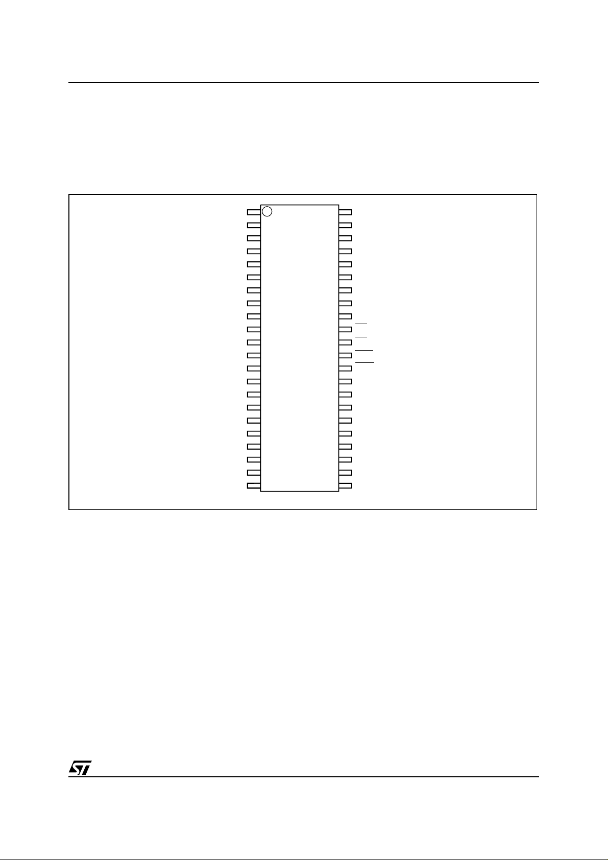
Figure 2. Logic Diagram Table 1. Signal Names
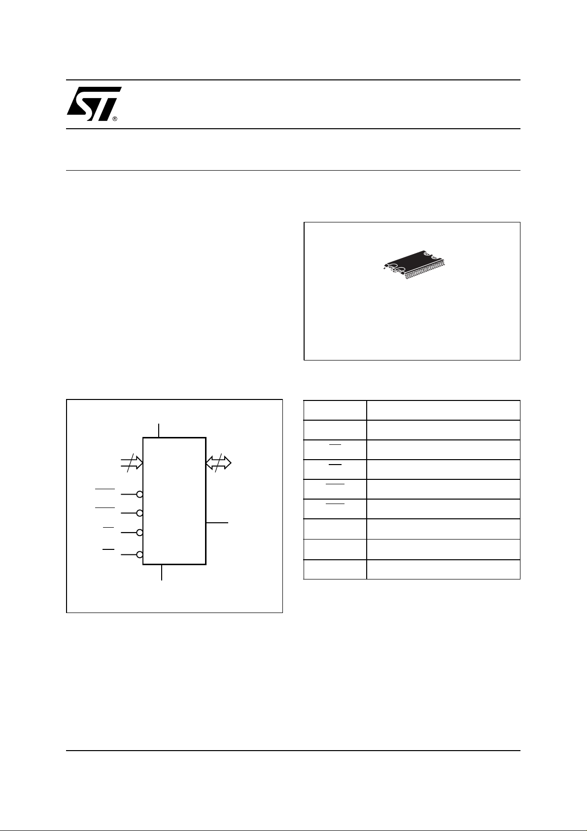
Figure 1. 44-pin, Hatless SOIC Package
44
SO44 (MH)
M616Z08
1
A0-A12
WE0
WE1
CE
OE
13
V
CC
M616Z08
V
SS
16
DQ0-DQ15
TO
AI04213
A0-A12 Address Inputs
DQ0-DQ15 Data Input/Output
CE
OE
WE0
WE1
V
CC
V
SS
TO Time-Out Pin
Note: TO Pin should be connected to VCC.
Chip Enable
Output Enable
WRITE Enable DQ 0-7
WRITE Enable DQ 8-15
Supply Voltage
Ground
1/14July 2002
Page 2

M616Z08
TABLE OF CONTENTS
DESCRIPTION ....................................................................3
44-pin Connec t ions (Figure 3.) . . . ..................................................3
MAXIMUMRATING.................................................................4
AbsoluteMaximumRatings(Table2.) ...............................................4
DC AND AC PARAM ETERS. . ........................................................5
DC and AC Measurement Conditions (Table 3.). . . .....................................5
AC Test ing Load Circuit (Figure 4.)..................................................5
Capacitance (Table 4.) . . . ........................................................5
DCCharacteristics(Table5.)......................................................6
OPERATION......................................................................6
READMode....................................................................6
AddressControlled,READModeACWaveforms(Figure5.)..............................6
Chip Enable or Output Enable Controlled, READ Mode AC Waveforms (Figure 6.). . ...........7
READModeACCharacteristics(Table6.)............................................7
WRITEMode...................................................................8
WRITE Enable Controlled, WRITE Mode AC W av eforms ( Figure 7.)........................8
ChipEnableControlled,WRITEModeACWaveforms(Figure8.)..........................8
WRITEModeACCharacteristics(Table7.)...........................................9
“Operational” Mode .............................................................10
NoiseImmunity................................................................10
WE(0,1)StatesduringAccess(Table8.)............................................10
Operating Modes (Table 9.).......................................................10
PARTNUMBERING...............................................................11
PACKAGE MECHANICAL INFORMATION . . . ..........................................12
REVISIONHISTORY...............................................................13
2/14
Page 3
DESCRIPTION
The M616Z08 is a 128 Kbit (131,072 bit) CMOS
SRAM, organized by 16 bits. The device features
fullystatic operation requiring noexterna l clocks or
timing strobes, with equal address access and cycle times. It requires a single 2.6V ± 10% or
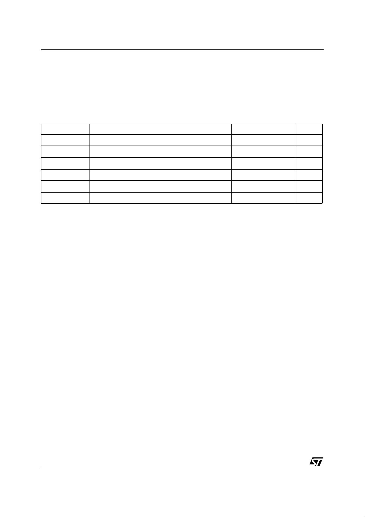
Figure 3. 44-pin Connections
M616Z08
3.3V ± 10% supply, and all inputs and outputs are
TTL compat ible.
The M616Z08 is available in a 44-lead SOIC package.
DQ0
DQ1
DQ2
DQ3
V
CC
V
SS
DQ4
DQ5
DQ6
DQ7
V
CC
V
SS
DQ8
DQ9
DQ10
DQ11
V
SS
V
CC
DQ12
DQ13
DQ14
DQ15
1
2
3
4
5
6
7
8
9
10
11
12
13
14
15
16
17
18
19
20
21
22
M616Z08
44
43
42
41
40
39
38
37
36
35
34
33
32
31
30
29
28
27
26
25
24
23
A12
A11
A10
A9
V
CC
V
SS
A08
A07
TO
CE
OE
WE1
WE0
A06
A05
A04
V
SS
V
CC
A03
A02
A01
A00
AI04212
Note: TO Pin should be connected to VCC.
3/14
Page 4
M616Z08
MAXIMUM RATING
Stressingthedeviceabovetheratinglistedinthe
“Absolute Maximum Ratings” table may caus e
permanent damage to the device. These are
stress ratings only and operation of the device at
these or any other conditions above those indicated in the Ope ra ting sections of this specification is
Table 2. Absolute Maximum Ratings
Symbol Parameter Value Unit
T
A
(1)
T
STG
(2,3)
V
IO
V
CC
(4)
I
O
P
D
Note: 1. Reflow at peak temperature of 215°C to 225°C for < 60 seconds (total thermal budget not to exceed 180°C for between 90 and 120
seconds).
2. Upto a maximum operating V
(min)= VSS–2.0VAC(pulsewidth≤10% t
3. V
IL
V
(max)= VCC+ 2.0V AC (pulse width ≤ 10% t
IH
4. Oneoutput at a time, not to exceed 1 second duration.
Ambient Operating Temperature –40 to 125 °C
Storage Temperature –65 to 150 °C
Input or Output Voltage
Supply Voltage –0.3 to 4.0 V
Output Current 10 mA
Power Dissipation 270 mW
of 3.6V only.
CC
AVAV
AVAV
(min))
(min))
not implied. Exposure to Absolute Maximum Rating conditions for extended periods may affec t device reliability. Refer also to the
STMicroelectronics SURE Program and other relevant quality documents.
–0.3 to V
CC
+ 0.3
V
4/14
Page 5
DC AND AC PARAM ETERS
This section summarizes the operating and measurement conditions, as well as the DC and AC
characteristics of the device. The parameters in
the following DC and AC Characteristic tables are
ment Conditions listed in the relevant tables. Designers should check that the operating conditions
in their projects match the measure ment conditions when using the quoted parameters.
derived from tests performed under the Measure-
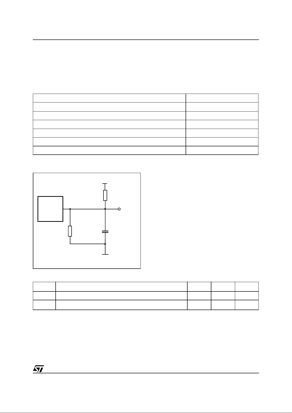
Table 3. DC and AC Measurement Conditions
Parameter M616Z08
Supply Voltage
V
CC
Ambient Operating Temperature –40 to 125°C
2.34 to 3.0V or 3.0 to 3.6V
M616Z08
Load Capacitance (C
Input Rise and Fall Times ≤ 5ns
Input Pulse Voltages 0to3V
Input and Output Timing Ref. Voltages 1.5V
Note: Output High Z is defined as the point where data is no longer driven.
)
L
50pF
Figure 4. AC Testing Load Circuit
3.0V
2.6 KΩ
DEVICE
UNDER
TEST
2.6 KΩ
OUT
CL = 50 pF
or 5pF
AI05650
Table 4. Capacitance
Symbol
C
C
OUT
Note: 1. Effective capacitance measured with power supply at 3.3V; sampled only, not 100% tested.
Input Capacitance on all pins (except DQ) 10 pF
IN
(3)
Output Capacitance 10 pF
2. A t 25°C; f = 1MHz.
3. Outputs deselected.
Parameter
(1,2)
Min Max Unit
5/14
Page 6

M616Z08
Table 5. DC Characteristics
Sym Parameter
I
Input Leakage Current
LI
I
Output Leakage Current
LO
(3)
I
CC1
I
CC3
Supply Current
Supply Current (Standby)
(4)
CMOS
Test Condition
0V ≤ VIN ≤ V
0V ≤ V
V
V
CC
CC
OUT
CC
= 3.6V,
CE ≥ VCC– 0.2V, f = 0
(1)
TO Pin
(2)
Min Typ Max Unit
65 125 µA
All other inputs ±1 µA
≤ V
=3.6V
CC
±1 µA
75 mA
1mA
V
Input Low Voltage –0.3
IL
V
V
0.7V
CC
CC
CC
–0.2V
–0.3V
V
Input High Voltage
IH
I
V
Output Low Voltage
OL
OL
= 1mA
2.34 to 3.0V
I
V
Note: 1. Valid for AmbientOperating Temperature:TA= –40 to 125°C; VCC= 3.0 to 3.6V or 2.34 to 3.0V (except where noted).
Output High Voltage
OH
2. I nput leakage on TO Pin due to internal pull-down to V
3. A verage AC current, Outputs open, cycling at t
4. A ll other Inputs at V
≤ 0.2V or VIH≥ VCC–0.2V.
IL
OH
= –1mA
minimum.
AVAV
3.0 to 3.6V
.
SS
0.3V
CC
VCC+ 0.3
0.2 V
OPERATION
READ Mode
The M616Z08 is in the READ Mode whenever
WRITE Enable (WE0
Enable (OE
) Low, and Chip Enable (CE) is assert-
or WE1) is High with Output
ed. This provides access to data from sixteen of
the 131,072 locations in the static memory array,
specified by the 13 address inputs. Valid data will
be available at the sixteen output pins wit hin t
AVQV
after the last stable address, providi ng OE is Low
and C
E is Low. If Chip Enable or Output Enable
access times are not met, data access wi ll be
measured from the limiting parameter (t
t
) rather than the address. Data out may be
GLQV
indeterminate at t
will always be valid at t
ELQX
and t
AVQV
, but data lines
GLQX
.
Figure 5. Address Controlled, READ Mode AC Waveforms
tAVAV
ELQV
V
V
V
or
A0-A12
DQ0-DQ15
Note: CE =Low,OE= Low, WE(0,1) =High.
6/14
VALID
tAVQV tAXQX
DATA VALID
AI04210
Page 7

Figure 6. Chip Enable or Output Enable Controlled, READ Mode AC Waveforms
tAVAV
M616Z08
A0-A12
tAVQV tAXQX
tELQV
CE
tELQX
tGLQV
OE
tGLQX
DQ0-DQ15
VALID
VALID
Table 6. READ Mode AC Characteristics
Symbol
t
AVAV
t
AVQV
t
ELQV
t
GLQV
t
ELQX
t
GLQX
t
EHQZ
t
GHQZ
t
AXQX
Note: 1. Valid for AmbientOperating Temperature:TA= –40 to 125°C (except where noted).
2. C
READ Cycle Time 36 20 ns
Address Valid to Output Valid 36 20 ns
Chip Enable Low to Output Valid 36 20 ns
Output Enable Low to Output Valid 20 10 ns
Chip Enable Low to Output Transition 0 0 ns
Output Enable Low to Output Transition 0 0 ns
(2)
Chip Enable High to Output Hi-Z 10 10 ns
(2)
Output Enable High to Output Hi-Z 10 10 ns
Address Transition to Output Transition 0 0 ns
= 5pF.
L
Parameter
(1)
2.34 to 3.0V 3.0 to 3.6V
Min Max Min Max
tGHQZ
M616Z08
–20
tEHQZ
AI05638
Unit
7/14
Page 8

M616Z08
WRITE Mode
TheM 616Z08 is in the WRITE mode whenever the
(low memory addresses) or WE1 (high mem-
WE0
ory addresses) and C
page 10). Either the Chip Enable input (C
WRITE Enable input (WE0
E pins are low (see Table 8,
E)orthe
or WE1) must be deasserted during Address transitions for subsequent WRIT E cycles. WRITE begins with the concurrence of Chip Enable being active with WE0
WE1
low. There fore, address setup t im e is referenced toWRITE Enable and Chip Enable ast
and t
respectively, and is determined by the
AVEH
or
AVWL
latter occurring edge.
Figure 7. WRITE Enable Controlled, WRITE Mode AC Waveforms
The WRITE cycle can be terminated by the e arlier
rising edge of C
if theOutput is enabled (C
then WE0
or WE1 will return the outputs to high
impedance within t
must be taken to avoid bus c ontention in this type
of operation. Dat a input must be v ali d for t
before the rising edge of WRITE Enable, or for t
before the rising edge of CE, whichever oc-
VEH
curs first, and remain valid f or t
Note: When using MCP555 with TO Pin high, re-
laxedWRITEtiming(CSNT=1inthechipselect
configuration register) should be selected.
tAVAV
E,orWE0/WE1.
E = Low and OE =Low),
of its falling edge. Care
WLQZ
WHDX
or t
EHDX
DVWH
D-
.
A0-A12
tAVEL
CE
tAVWL
WE (0,1)
tWLQZ
DQ0-DQ15
VALID
tAVWH
tWLWH
DATA INPUT
tDVWH
Figure 8. Chip Enable Controlled, WRITE Mode AC Waveforms
tAVAV
A0-A12
tAVEL
VALID
tAVEH
tELEH
tWHAX
tWHQX
tWHDX
AI04211
tEHAX
CE
WE (0,1)
DQ0-DQ15
Note: 1. Output Enable (OE) = High.
8/14
goes High with WE0 or WE1 high, the output remains in a high-impedance state.
2. I f CE
tAVWL
tEHDX
DATA INPUT
tDVEH
AI05639
Page 9

Table 7. WRITE Mode AC Characteristics
M616Z08
M616Z08
Symbol
Parameter
(1)
2.34 to 3.0V 3.0 to 3.6V
Min Max Min Max
t
AVAV
t
AVWL
t
AVWH
t
AVEH
t
WLWH
t
WHAX
t
WHDX
t
WHQX
t
WLQZ
t
AVEL
t
ELEH
t
EHAX
t
EHDX
t
DVWH
t
DVEH
Note: 1. Valid for AmbientOperating Temperature:TA= –40 to 125°C (except where noted).
2. C
3. A t any given temperature and voltage condition, t
WRITE Cycle Time 36 20 ns
Address Valid to WRITE Enable Low 2 2 ns
Address Valid to WRITE Enable High 34 18 ns
Address Valid to Chip Enable High 34 18 ns
WRITE Enable Pulse Width 25 11 ns
WRITE Enable High to Address Transition 2 2 ns
WRITE Enable High to Input Transition 2 2 ns
(3)
WRITE Enable High to Output Transition 0 0 ns
(2,3)
WRITE Enable Low to Output Hi-Z 10 10 ns
Address Valid to Chip Enable Low 2 2 ns
Chip Enable Low to Chip Enable High 25 11 ns
Chip Enable High to Address Transition 2 2 ns
Chip Enable High to Input Transition 2 2 ns
Input Valid to WRITE Enable High 20 8 ns
Input Valid to Chip Enable High 20 8 ns
= 5pF
L
WLQZ
is less than t
for any given device.
WHQX
–20
Unit
9/14
Page 10

M616Z08
“Operational” Mode
The M616Z08 has a Chip Enable power down feature which invokes an automatic standby mode
whenever Chip Enableis de-asserted (C
An Output Enable (OE
) signal provides a high
E =High).
speed tri-state control,allowing fast READ/WRITE
cycles to be achieved with the common I /O data
bus. Operational modes are determined by device
control inputs WE0
or WE1 and CE as summa-
rized in “ Operating Modes” (see Table 8 and Table
9).
Table 8. WE(0,1)
WRITE Enable Used during 16-bit Port Access
States during Access
WE0
WE1
WRITE Enable for DQ (0-7)
WRITE Enable for DQ (8-15)
Noise Immunity
When designing with high speed mem ory , proper
power trace layout and capacitive decoupling
must bemaintained toensure proper system operation.Power and ground line inductance s hould be
reduced by providing separate power planes. The
impedance of the decoupling path from t he power
pin through the decoupling capacitor should also
be kept to a minimum. Sm all decoupling capacitors (10nF) should be located as close to the device pins as possible to limit the high frequency
noise. Larger capacitor values (10uF and 1uF) are
recommended to reduce low frequency noise and
should be placed next to t he power entry point of
the board. Proper line termination should al s o be
employed to minimize signal reflection.
See Motorola Semiconductor Application Note
AN2127/D for additional Electromagnetic Compa tibility (EMC) system design guidelines.
Table 9. Operating Modes
Operation CE
Deselect
Word WRITE
Byte 0 WRITE
Byte 1 WRITE
Byte 0 WRITE, Byte 1 READ
Byte 1 WRITE, Byte 0 READ
Word READ
Note: 1. X = '1' or '0'
OE WE0 WE1 DQ0–DQ7 DQ8–15
V
IH
V
IL
V
IL
V
IL
V
IL
V
IL
V
IL
(1)
X
V
IH
V
IH
V
IH
V
IL
V
IL
V
IL
(1)
X
V
IL
V
IL
V
IH
V
IL
V
IH
V
IH
(1)
X
V
IL
V
IH
V
IL
V
IH
V
IL
V
IH
Hi-Z Hi-Z
Hi-Z Hi-Z
Hi-Z Hi-Z
Hi-Z Hi-Z
Hi-Z Data
Data Hi-Z
Data Data
10/14
Page 11

M616Z08
PART NUMBERING
Table 10. Ordering Information Example
Example: M6 16Z08 –20 MH 3 TR
Device Type
M6
Device Function
16Z08 = 128Kbit (8 x16)
Speed
–20 = 20ns (3.0 to 3.6V)
Package
MH = 44-lead, Hatless SOIC
Temperature Range
3 = –40 to 125°C
Shipping Method for SOIC
blank = Tubes
TR = Tape & Reel
For a list of available options (e.g., Speed, Package) or for further information on any as pec t of this device,
please contact the ST Sales Office nearest to you.
11/14
Page 12

M616Z08
PACKAGE MECHANICAL INFORMATION
Figure 9. SO44 – 44-Lead, Plastic, Hatless, Small Package Outline
A2
A
Be
CP
D
N
E
H
1
SOH-C
Note: Drawing is not to scale.
Table 11. SO44 – 44-lead, Plastic, Hatless, Small Package Mechanical Data
Symb
Min Typ Max Min Typ Max
mm inches
C
LA1 α
A 3.05 0.120
A1 0.05 0.36 0.002 0.014
A2 2.34 2.69 0.092 0.106
B 0.36 0.46 0.014 0.018
C 0.15 0.32 0.006 0.012
D 17.71 18.49 0.697 0.728
E 8.23 8.89 0.324 0.350
e 0.81 – – 0.032 – –
H 11.51 12.70 0.453 0.500
L 0.41 1.27 0.016 0.050
a0°8°0°8°
N44 44
CP 0.10 0.004
12/14
Page 13

REVISION HISTORY
Table 12. Document Revision History
Date Rev. # Revision Details
September 2001 1.0 First Issue
11/1901 2.0
02/12/02 2.1 Add TO Pin (Figure 2, 3, Table 1); change WRITE Mode AC Characteristics (Table 7)
02/21/02 2.2 Changes for TO Pin (Table 5) and change characteristics (Table 6, 7)
05/13/02 2.3 Add reflow time and temperature footnote (Table 2)
07/22/02 2.4 Add “Hatless” to package description (Figure 1, 9 and Table 10, 11)
Correction of Operating Modes text (Table 9); document status changed to “Data Sheet;”
add text for Noise Immunity (page 10)
M616Z08
13/14
Page 14

M616Z08
Automotive, Automotive, Automotive, Aut omotive, Automotive, Automot ive, Autom otive, Automot ive, Automotive, Automotive, Automotive, Automotive, Automotive, Automotive, Automotive, Low, Power, Low,
Power, Low, Power, Low, P ower, Low, Power, Low, Power, Low, Power, Low, Power, Low, Power, Low,
Power, Low, Power, Low, Power, Low, Power, Low, Power, Low, Power, SRAM, SRAM, SRAM, SRAM,
SRAM, SRAM, SRAM, SRAM, SRAM, SRAM, SRAM, SRAM, SRAM, SRAM, SRAM, LPSRAM,
LPSRAM,LPSRAM, LPSRAM,LPSRAM,LPSRAM, LPSRAM,LPSRAM, LPSRAM, LPSRAM,LPSRAM,
LPSRAM, LPSRAM, LPSRAM, LPSRAM, Auto, Auto, Auto, Auto, Auto, Auto, Auto, Auto, Auto, Auto, Auto, Auto, A uto, Auto, Auto, Auto, Auto, Auto,Aut o, Aut o, High, Temperature,Temp, Range, High, Temperature, T emp, Range, High, Temperature, Temp, Range, High, Temperature, Temp, Range, High,
Temperature, Temp, Range, High , Temperature, T emp, Range, High, Temperature, Tem p, Range, High,
Temperature, Temp, Range, High, Temperature, Temp, Range, High, Temperature, Temp, Range
Information furnished is believed to be accurate and reliable. However, STMicroelectronics assumes no responsibility for the consequences
of use ofsuch information nor for any infringement of patents or other rightsof third parties which may result from its use. No licenseis granted
by implication or otherwise under any patent or patent rights of STMicroelectronics. Specifications mentioned in this publication are subject
to change without notice. This publication supersedes and replaces all information previously supplied. STMicroelectronics products are not
authorized for use as critical components in life support devices or systems without express written approval of STMicroelectronics.
The ST logo is registered trademark of STMicroelectronics
All other names are the property of their respective owners.
© 2002 STMicroelectronics - All Rights Reserved
Australia - Brazil - Canada - China - Finland - France - Germany - Hong Kong - India - Israel - Italy - Japan - Malaysia -
Malta - Morocco - Singapore - Spain - Sweden - Switzerland - United Kingdom - U.S.A.
14/14
STMicroelectronics GROUP OF COMPANIES
www.st.com
 Loading...