

Page 1
MITSUBISHI ICs (TV)
M61203CFP
NTSC TV SIGNAL PROCESSOR
DESCRIPTION
The M61203CFP is desinged to provide a solution to NTSC color television system. It is an I2C bus
controlled NTSC 1 chip.
It consists of various processing blocks such as power supply, video IF, sound IF, luminance,
chrominance, OSD display, interface, H and V deflection.
At each block, I2C control is possible and a total of 62 parameters can be controlled by I2C bus.
FEATURES
Various signal output for Intelligent Monitoring function
Alignment-free sound demodulator
Built-in H OSC resonator
Built-in sync sep.(auto-slicer type)
Built-in black peak hold capacitor
ACL / ABCL
Vertical count-down circuit
Built-in vertical saw tooth generator
Mute filter integrated
PLL-SPLIT SIF system with FM recieving function
H&V pulse output for OSD
Built-in MCU reset circuit
fsc output
Built-in 5V(MCU,1CHIP) & 8V regulator
RECOMMENDED OPERATING CONDITIONS
Supply voltage 4.75V to 5.25V (pins 2, 3 , 23 and 24)
7.6V to 8.4V (pins 18, 19, 44, and 45)
8.3V to 9.1V (pin 55)
Rated supply voltage 5.0V (pins 2, 3, 23 and 24)
8.0V (pins 18, 19, 44 and 45)
8.7V (pin 55)
Maximum output current 4.0mA (pin 7)
APPLICATION
NTSC type color TV, projecter
MITSUBISHI
ELECTRIC
1
Page 2
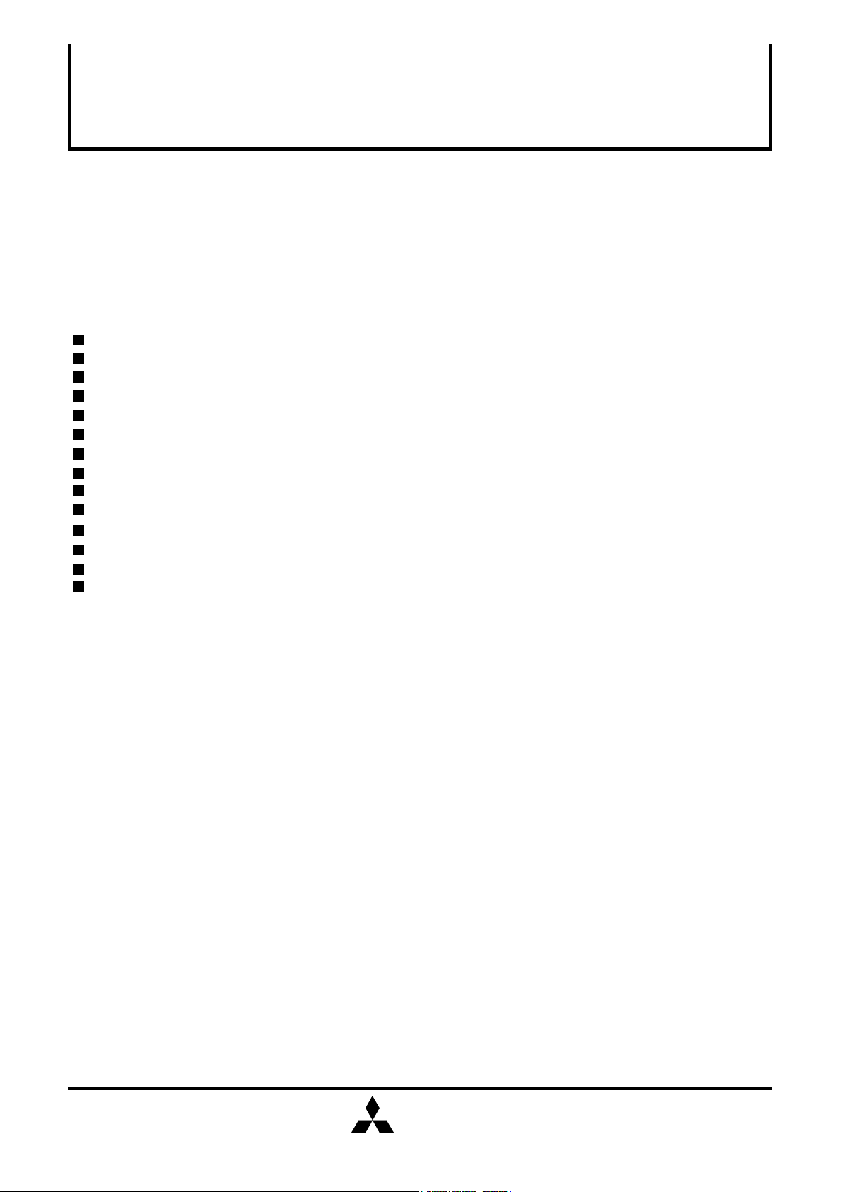
PIN CONFIGURATION (TOP VIEW)
MITSUBISHI ICs (TV)
M61203CFP
NTSC TV SIGNAL PROCESSOR
VIF IN(2)
VIF VCC(1)
VIF VCC(2)
H.VCO FEED BACK
SCL
FBP IN
H OUT
DEF GND(1)
DEF GND(2)
SDA
AFC FILTER
INV FBP OUT
POWER ON CONTROL IN
R OUT
G OUT
B OUT
10
11
12
13
14
15
16
IF AGC FILTER 2
1
2
3
4
5
6
7
8
9
M61203CFP
48
LIMTER IN
47
SWTCHING REG CONTROL
46
Hi VCC(2)
45
Hi VCC(1)
44
INTELLIGENT MONITOR
43
MCU RESET
42
MCU 5.7VREG OUT
41
Y SW OUT
40
5.7VREGOUT
39
VIDEO/CHROMA GND(2)
38
VIDEO/CHROMA GND(1)
37
TV/Y IN
36
CHROMA APC FILTER
35
EXT/C IN
34
8.7VREG OUT
33
MITSUBISHI
ELECTRIC
2
Page 3
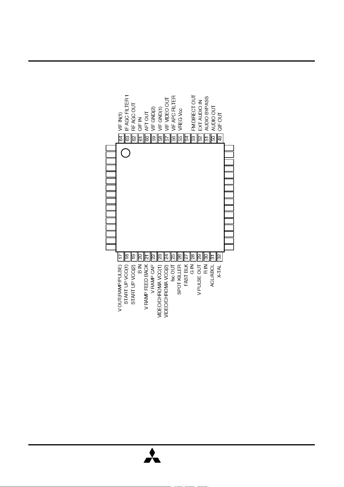
BLOCK DIAGRAM
MITSUBISHI ICs (TV)
M61203CFP
NTSC TV SIGNAL PROCESSOR
MITSUBISHI
ELECTRIC
3
Page 4
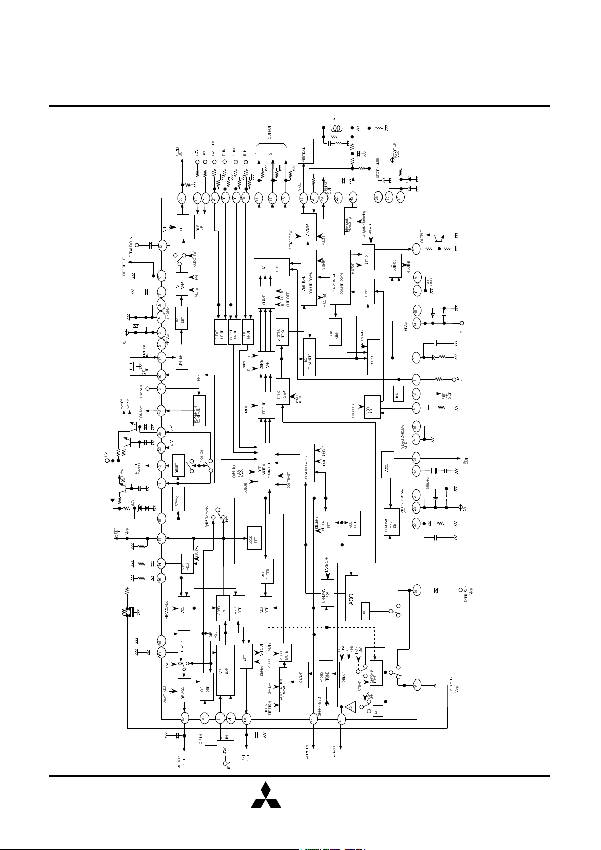
ABSOLUTE MAXIMUM RATINGS
MITSUBISHI ICs (TV)
M61203CFP
NTSC TV SIGNAL PROCESSOR
Symbol
Vcc
Pd
Kt
Topr
Tstg
Supply voltage
Power dissipation
Thermal derating
Operating temperature
Storage temperature
Parameter
TYPICAL CHARACTERISTICS
THERMAL DERATING (MAXIMUM RATING)
2.0
1.5
1.33
1.0
0.90
0.5
Ratings
6.0, 10.0
1325
10.6
-20 to 65
-40 to 150
Unit
V
mW
mW/oC
o
C
o
C
0 25 50 75 100 125 150
AMBIENT TEMPERATURE Ta (oC)
65
MITSUBISHI
ELECTRIC
4
Page 5
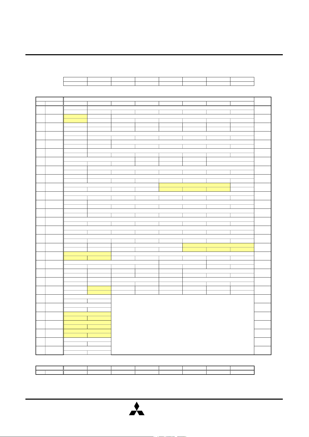
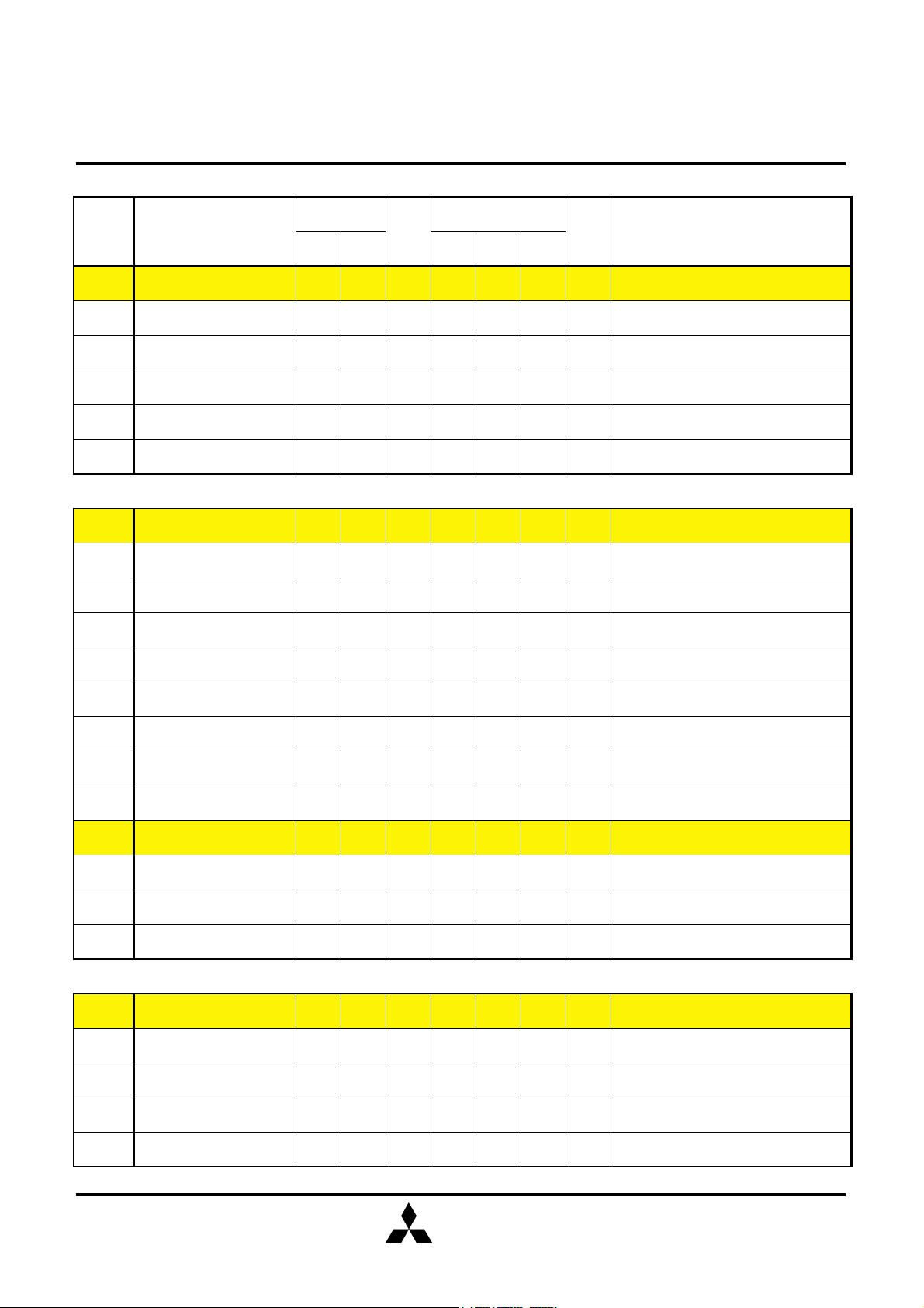
I2C Bus Table
MITSUBISHI ICs (TV)
M61203CFP
NTSC TV SIGNAL PROCESSOR
(1) SLAVE ADDRESS= BAH(WRITE), BBH(READ)
A6 A5 A4 A3 A2 A1 A0 R/W
1 0 1 1 1 0 1 1/0
(2) WRITE TABLE(input bytes)
SUB ADDRESS
HEX BIN D7 D6 D5 D4 D3 D2 D1 D0 INITIAL
00H 00000000 0 1 0 0 0 0 0 0 40H
01H 00000001 0 0 1 0 0 0 0 0 20H
02H 00000010 0 0 0 0 0 0 0 0 00H
03H 00000011 0 0 0 0 0 0 0 0 00H
04H 00000100 0 0 V1 V0 V0 V0 V0 V0 20H
05H 00000101 V0 V1 V0 V0 V0 V0 V0 V0 40H
06H 00000110 1 0 0 V0 0 V0 0 0 80H
07H 00000111 0 V1 V0 V0 V0 V0 V0 V0 40H
08H 00001000 V0 V1 V0 V0 V0 V0 V0 V0 40H
09H 00001001 1 1 1 1 1 0 0 0 F8H
0AH 00001010 V1 V0 V0 V0 V0 V0 V0 V0 80H
0BH 00001011 0 1 0 0 0 0 0 0 40H
0CH 00001100 0 1 0 0 0 0 0 0 40H
0DH 00001101 1 0 0 0 0 0 0 0 80H
0EH 00001110 1 0 0 0 0 0 0 0 80H
0FH 00001111 1 0 0 0 0 0 0 0 80H
10H 00010000 0 0 1 0 0 1 0 0 24H
11H 00010001 0 0 1 0 0 0 0 0 20H
12H 00010010 0 0 0 0 0 0 0 0 00H
13H 00010011 0 0 0 0 0 0 0 0 00H
14H 00010100 0 0 0 0 0 1 0 0 04H
15H 00010101 0 1 0 0 0 0 0 0 40H
16H 00010110 0 0 00H
17H 00010111 0 0 00H
18H 00011000 0 0 00H
19H 00011001 0 0 00H
1AH 00011010 0 0 00H
1BH 00011011 0 0 00H
1CH 00011100 0 0 00H
DATA
SPLIT RF Delay Adj
(not asigned) VIFFreq5875 VIF VCO ADJ
Video Mute Audio EXT Force S.Killer TRAP Off Video T Soft ABCL Y DL Fine Adj Take Off
Audio Mute Audio ATT
ABCL Gain AFT Defeat Video Tone
EXTRGB C. Clip
VIF Video Out Gain Y/C
VIF Defeat Tint Control
Blue Back Color Control
AFC2 H Phase (not asigned) AFC2 Gain
V-free Drive(R)
FM Radio Drive(B)
White Back
H-free V.1Window AFC Gain H Start Service SW V Shift
FBP Vth L YSW LPF Black Strech Charge
H Phase MSB (not asigned) fsc free Analog OSD Force MONO Force COLOR C.Angle 95 Killer level
Black Strech Discharge
S.Slice Down1
(inhibited) V-Size
Monitoring Gamma Control TRAP Fine Adj
Test
Test
(not asigned)
(not asigned)
(not asigned)
Test
H VCO Adj (not asigned)
Contrast Control
Black Stretch Off
Brightness Control
Cut Off(R)
Cut Off(G)
Cut Off(B)
S.Slice Down2
EXT Y DL Time Adj
FM Station Level
NOTE: V0 / V1 ==> V- LATCH BIT
(3) READ TABLE (output bytes)
SUB ADDRESS
00H 00000000 KILLERB FM STDETB VCOINB STDETB AFT0 AFT1 HCOINB (not asigned)
D7 D6 D5 D4 D3 D2 D1 D0
MITSUBISHI
ELECTRIC
5
Page 6
MITSUBISHI ICs (TV)
M61203CFP
NTSC TV SIGNAL PROCESSOR
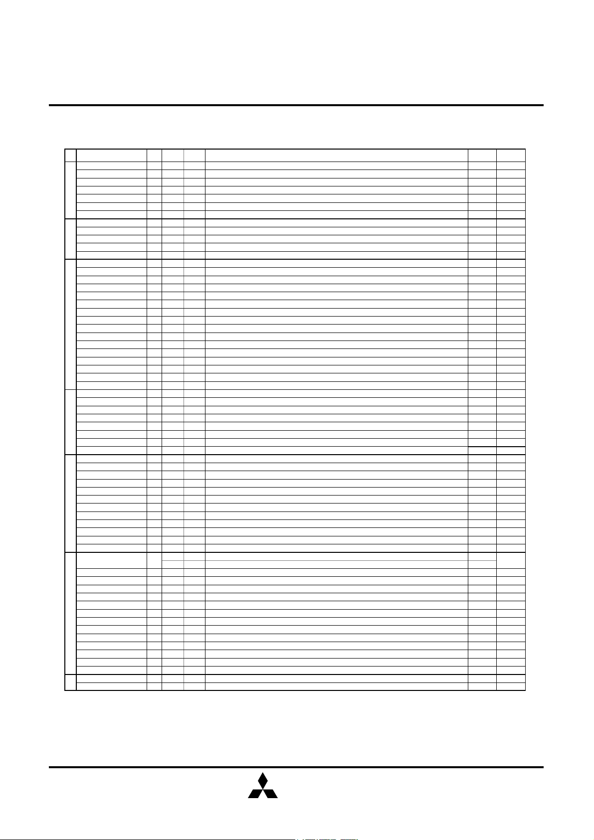
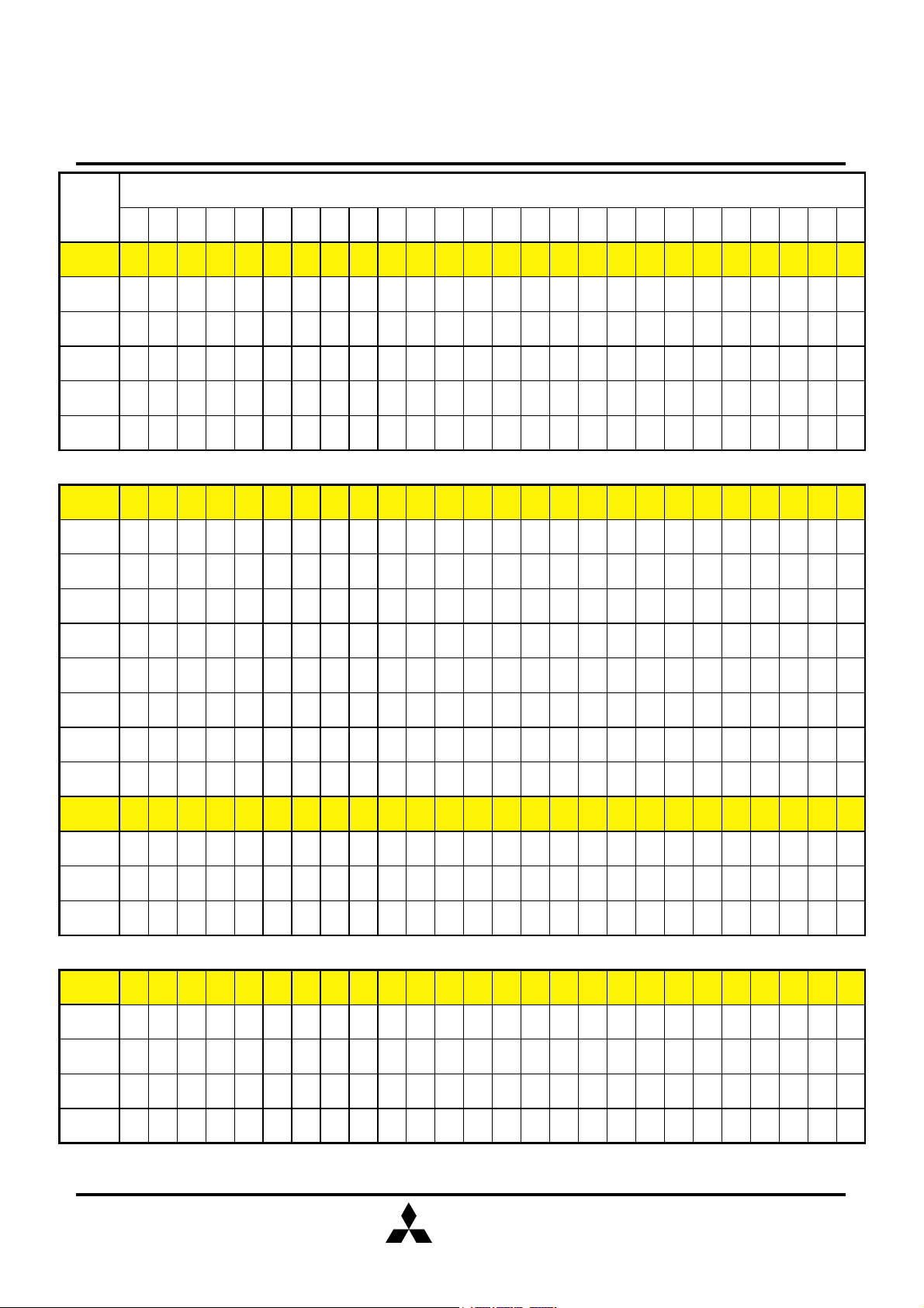
(4) Bus function
WRITE
FUNCTION BIT SUB ADD DATA DISCRIPTION INITIAL NOTE
RF Delay Adj 7 00H D0-D6 RF AGC Delay Point Adjustment by 7bit DAC 1000000
VIF VCO Adj 6 10H D0-D5 VIF VCO Free-running Frequency Adjustment by 5bit DAC 100000
VIF Freq 58.75 1 01H D6 VIF Frequency Selector 0: 45.75MHz, 1: 58.75MHz 000
VIF Video Out Gain 3 06H D5-D7 VIF Video det output Amplitude Adjustment by 3bit DAC 100
AFT Defeat 1 04H D6 AFT OUT ON/OFF(Defeat) switch 0: AFT ON (Non Defeat), 1: Defeat 0
VIF Defeat 1 07H D7 VIF AGC Gain Normal/Minimum switch 0: AGC Function, 1: Defeat(Minimum Gain) 0
SPLIT 1 00H D7 Inter Carrier/Split Carrier Switch 0: Inter Carrier, 1: Split Carrier 0
Audio ATT 7 03H D0-D6 Audio Out Level Attenuation by 7bit DAC MAX gain=0dB 0
Audio EXT 1 02H D6 AF Direct out/External Audio input signal switch 0: AF amp out, 1: External 0
SIF VIFDEF RGB VIDEOCHROMA
Audio Mute 1 03H D7 AF Direct out ON/OFF(Mute) switch 0: Sound ON (Non Mute), 1: Mute 0
FM Radio 1 0CH D7 TV / FM Radio switch 0: TV mode, 1: FM Radio mode 0
FM Station Level 3 14H D0-D2 FM Radio station detection level 100
Video Tone 6 04H D0-D5 Delay line type Aperture Control 100000 V Latch
Contrast Control 7 05H D0-D6 Contrast Control by 7bit DAC 1000000 V Latch
EXTRGB Contrast Clip 1 05H D7 Contrast Control Clip Switch when OSD mode 0: Clip ON, 1: Clip OFF 0 V Latch
Y DL Time Adj 2 06H D0-D1 Luminance Signal Delay time Adjustment 0
Y DL Fine Adj 1 02H D1 Luminance Signal Delay time Fine pitch Adjustment 0
EXT 1 06H D2 AV Switch Selector 0: TV mode, 1: EXT mode 0 V Latch
Y/C 1 06H D4 AV Switch Selector 0: Composit video input, 1: Y/C input mode 0 V Latch
Y SW LPF 1 14H D6 Y SW OUT frequency switch 0: FLAT, 1: LPF(fc=700KHz) 0
Video Tone Sharp 1 02H D3 Video Tone Gain (Hi/Normal) switch 0: normal, 1: high(sharp) 0
Video Mute 1 02H D7 Luminance signal Mute ON/OFF switch 0: OUT, 1: Mute 0
TRAP Off 1 02H D4 Chroma Trap ON/OFF switch 0:Chroma Trap ON, 1: Chroma Trap Off 0
TRAP Fine Adj 2 12H D0-D1 Chroma Trap fo Adjustment 00
Black Stretch Off 1 06H D3 Black Stretch function ON/OFF switch 0: ON, 1: OFF 0
Black Stretch Charge 2 14H D4-D5 Charge Time Constant Adjustment for Black Stretch 00
Black Stretch Discharge 2 1CH D6-D7 Discharge Time Constant Adjustment for Black Stretch 00
Gamma Control 2 12H D2-D3 Luminance Gamma Threshold Control 0:Gamma OFF 00
Tint Control 7 07H D0-D6 Tint Control by 7bit DAC. 1000000 V Latch
Color Control 7 08H D0-D6 Color Saturation Control by 7bit DAC. 1000000 V Latch
Take Off 1 02H D0 Chroma BPF/Take Off Switch 0 :BPF, 1: Take Off 0
C Angle95 1 15H D1 Chroma Demodulation Angle Switch 0: 103deg, 1: 95deg 0
Killer Level 1 15H D0 Color Killer Sensitivity Threshold Switch 0: 43dB, 1: 45dB 0
Force Color 1 15H D2 Forced Color mode switch 0:OFF, 1: Forced Color 0
Force Mono 1 15H D3 Forced B/W mode 0: OFF, 1: Forced Black&White 0
Fsc Free 1 15H D5 Free-running mode of crystal oscillator 0: OFF, 1: Free-running 0
Brightness Control 8 0AH D0-D7 Brightness Control by 8bit DAC 10000000 V Latch
Drive(R) 7 0BH D0-D6 R OUT Amplitude Adjustment by 7bit DAC 1000000
Drive(B) 7 0CH D0-D6 B OUT amplitude Adjustment by 7bit DAC 1000000
Cut Off(R) 8 0DH D0-D7 R OUT Pedestal Level Adjustment by 8bit DAC 10000000
Cut Off(G) 8 0EH D0-D7 G OUT Pedestal Level Adjustment by 8bit DAC 10000000
Cut Off(B) 8 0FH D0-D7 B OUT Pedestal Level Adjustment by 8bit DAC 10000000
Blue Back 1 08H D7 Blue Back mode ON/OFF switch 0: OFF, 1: Blue Back 0
White Back 1 10H D7 White Raster mode ON/OFF switch 0: OFF, 1: White Back 0
ABCL 1 02H D2 ABCL ON/OFF switch 0: OFF(ACL), 1: ABCL ON 0
ABCL Gain 1 04H D7 ABCL Gain Low/High switch 0: Low, 1: Hi 0
Force S.Killer 1 02H D5 Forced Spot Killer under Power on condition 1: OFF, 0: Forced S.Killer 0
Analog OSD 1 15H D4 OSD Input Digital/Analog switch 0: Digital, 1: Analog 0
AFC2 H Phase 5 09H D4-D7 Horizontal Phase Adjustment by 5bit DAC 1111
(H Phase MSB) 15H D7 (AFC2 H Phase MSB bit) 0
Service SW 1 13H D3 0: Vertical output ON/ Contrast Control Normal, 1: Vertical output OFF/Contrast Control Minimum 0
H Stop 1 13H D4 Horizontal output switch 0: H OUT, 1: H STOP 0
AFC Gain 1 13H D5 Horizontal AFC Gain switch 0: Low, 1: High 0
AFC2 Gain 1 09H D1 Horizontal AFC2 Gain switch 0: High, 1: Low 0
H VCO Adj 3 10H D3-D5 H VCO free-running frequency Adjustment 100
V Shift 3 13H D0-D2 V RAMP Sart timing Adjustment 2Line/Step 0
V-Size 6 11H D0-D5 V RAMP Amplitude Adjustment by 6bit DAC. 100000
H-free 1 13H D7 Horizontal Forced free-running mode switch 0: OFF, 1: Forced Free-running 0
V-free 1 0BH D7 Vertical Forced free-running mode switch 0: OFF, 1: Forced Free-running 0
S Slice Down 1 1 14H D3 Sync Det Slice Level (50%/30%) 0: 50%, 1: 30% 0
S Slice Down 2 1 10H D6 Sync Det Slice Level (50%/40%) 0: 50%, 1: 40% 0
FBP Vth L 1 14H D7 Pin6 FBP slice level switch 0:Vth=2V(narrow), 1:Vth=1V(wide) 0
1 Window 1 13H D6 Vertical Sync. Det mode (1 Window/2 Window) 0: 2 Window/Vsyncdet=9µs , 1: 1Window/Vsyncdet=11µ s 0
Monitoring 4 12H D4-D7 Intelligent Monitor mode selector 0000
Test - - NO USE for CUSTOMER (TEST MODE ) 0
MITSUBISHI
ELECTRIC
6
Page 7
READ
KILLERB 1 00H D7 Killer off for manual mode.
AFT0 1 00H D3 AFT output
AFT1 1 00H D2 AFT output
HCOINB 1 00H D1 Horizontal mute det output. 0: H coincident
FM STDETB 1 01H D4 Station det for FM Radio mode. 0: Station det.
VCOINB 1 01H D3 Vertical Sync det output. 0:V coincident
STDETB 1 01H D2 Station det for TV mode. 0: Station det.
<READ BYTE: AFT OUTPUT>
AFT0
AFT1
1
1
fo
0
1
+100KHz-100KHz
0
0
1
0
MITSUBISHI ICs (TV)
M61203CFP
NTSC TV SIGNAL PROCESSOR
IF
MITSUBISHI
ELECTRIC
7
Page 8
P14
P15
P16
P11
P12
P10P5P6
P7
P4
P17
P31
P29
P26
P22
P21
P25
P33
P39
P40
P35
P41
P42
P40
P50
P49
P63
P52
P51
P53
P54
P57
P60
P62
P5750AAA
P27
P46
A
Measurement circuit
MITSUBISHI ICs (TV)
M61203CFP
NTSC TV SIGNAL PROCESSOR
SIF IN
EXT R IN
75
0.1µ
0.015µ
33
34
35
8.2K
1µ
0.1µ
75
4.7K
36
37
38
39
40
41
10K
50
47µ
0.01µ
4.7K
0.01µ
0.01µ
+
42
43
44
45
46
47
48
EXT G IN
FASTBLK IN
M61203CFP
17181920212223242526272829303132
16
15
14
13
12
11
10
9
2.2K
2.2K
2.2K
SW11
SW13
0.01µ
1µ6.8K
100
8
7
6
5
4
3
0.01µ
10K
SCL
100
2K
0.1µ
2
1
47µ
64636261605958575655545352515049
VR 20K
1162153144135126117108
M74LS221P
9
4700p
MITSUBISHI
ELECTRIC
8
Page 9
INPUT SIGNALS
(1) For VIF/SIF block
MITSUBISHI ICs (TV)
M61203CFP
NTSC TV SIGNAL PROCESSOR
SG No.
SG 1
SG 2
SG 3
SG 4
SG 5
SG 6
SG 7
SG 8
SG 9
SG 10
SG 11
SG 12
SG 13
SG 14
Input signal (value at pin terminal is 50ohm)
fo=45.75MHz, 90dBµ, fm=20kHz, AM77.8%
fo=58.75MHz, 90dBµ, fm=20kHz, AM77.8%
fo=45.75MHz, 90dBµ, CW
f1=45.75MHz, 90dBµ, CW
f2=45.75 +/-4.5MHz, 70dBµ, CW
fo=45.75MHz, amplitude can be varied, fm=20kHz, AM77.8%
fo=45.75MHz, amplitude can be varied, fm=20kHz, AM16%
fo=45.75MHz, 80dBµ, fm=20kHz, CW
fo=45.75MHz, 110dBµ, fm=20kHz, CW
fo=40.75 to 50.75MHz (frequency can be varied), 90dBµ, CW
fo=44.75MHz, 90dBµ, CW
fo=46.75MHz, 90dBµ, CW
fo=53.75 to 63.75MHz(frequency can be varied), 90dBµ, CW
f1=45.75MHz, 90dBµ, Red raster signal, AM=87.5% video modulation,
f2=4.5MHz, CW, P/S=20dB
fo=45.75MHz, Standard 10-step signal, Sync ratio 28.6%
AM=87.5% video modulation, Sync tip-Sync tip level 90dBµ
SG 15
SG 16
SG 17
SG 18
SG 19
SG 20
SG 21
SG 22
SG 23
fo=45.75MHz, 93dBµ, CW
fo=45.75MHz, 73dBµ, CW
fo=4.5MHz, 100dBµ, fm=400Hz, FM +/-25kHz dev.
fo=4.5MHz, 100dBµ, fm=400Hz, AM 30%
fo=4.5MHz, 100dBµ, CW
fo=400Hz, 500mVrms, CW
fo=0.5 to 8.5MHz, 100dBµ, fm=400Hz, FM +/-25kHz dev.
fo=41.25MHz, amplitude can be varied, CW
fo=41.25MHz, 85dBµ, fm=400Hz, FM +/-75kHz dev.
MITSUBISHI
ELECTRIC
9
Page 10
NTSC TV SIGNAL PROCESSOR
standard
video signal.
The vertical signal should be
interlaced at 60Hz.
by
signal SG. A. The typical amplitude
is 0.714mVp-p.
The frequency of Luminance, ( f )
as stated in test.
(2) VIDEO/CHROMA/RGB/DEF block
SG No. Input signal (value at pin terminal is 50ohm)
NTSC system APL100%
MITSUBISHI ICs (TV)
M61203CFP
SG. A
SG. B
SG. C
The amplitude and frequency of
Luminance signal can be varied
NTSC system standard monochroma video signal.
The vertical signal should be
interlaced at 60Hz.
0.286V
4.7µs
1.5µs 5.8µs
4.7µs
1.5µs 5.8µs
4.7µs
0.286V
0.714V
1Vp-p
0.286V
f
0.572V
NTSC system video signal. APL
can be varied.
The vertical signal should be
SG. D
interlaced at 60Hz.
4.0µs
1.5µs 5.8µs
MITSUBISHI
ELECTRIC
4.7µs
1.5µs5.8µs
Vy
0.286V
10
Page 11
MITSUBISHI ICs (TV)
M61203CFP
NTSC TV SIGNAL PROCESSOR
SG No. Input signal (value at pin terminal is 50ohm)
NTSC system mono-chroma video signal. The
SG. E
SG. F
amplitude and frequency of burst part and
chroma part can be varied.
The vertical signal should be interlaced at
60Hz.
typical condition:
Veb=0.286V, Vec=0.572V
feb=fec=3.579545MHz
Fast blanking signal.
It should be synchronized with input video
signal.
External RGB (OSD) signals.
They should be synchronized with input
video signal and fast blanking signal.
Veb
0.286V
0V
0V
4.7µs
feb fec
20µs 24µs
20µs 24µs
Vec
1.5µs5.8µs
2.0V
Vosd
SG. G
SG. H
SG. I
SG. J
NTSC system rainbow color bar video signal.
The vertical signal should be interlaced at 60Hz.
Duty cycle 90%, frequency can be varied, level can be varied (typ. 1Vp-p)
1Vp-p
Duty cycle can be varied (typ. 95%), frequency can be varied, level can be
varied (typ. 1Vp-p)
1Vp-p
NTSC system standard color bar
video signal.
4.7µs
0.714V
The vertical signal should be
interlaced at 60Hz.
SG. K
1.5µs 5.8µs
NTSC system standard 8-steps signal.
The vertical signal should be interlaced at 60Hz.
MITSUBISHI
ELECTRIC
0.286V
11
Page 12
MITSUBISHI ICs (TV)
M61203CFP
NTSC TV SIGNAL PROCESSOR
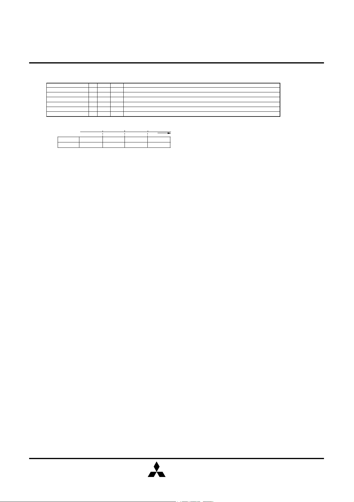
Setup instruction for evaluation PCB
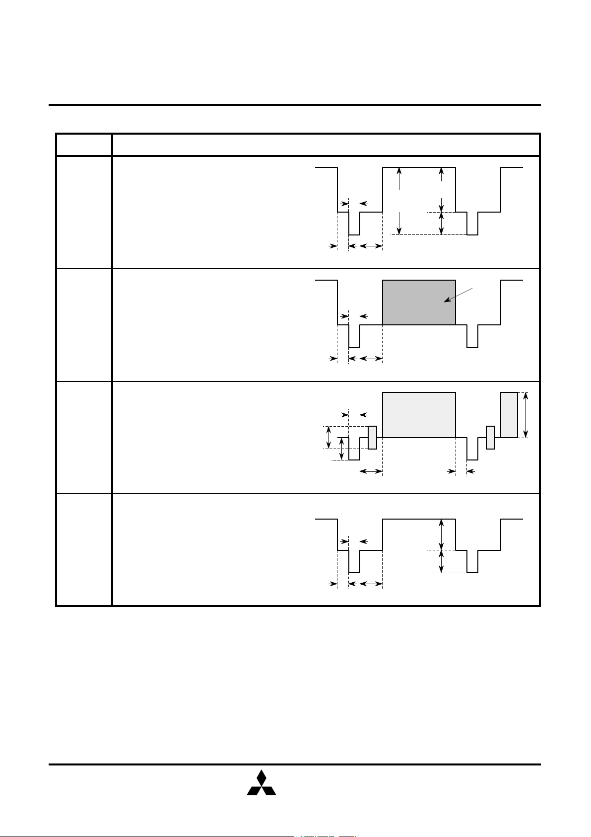
(1) Horizontal blanking pulse adjustment
The timing and pulse width of the horizontal blanking pulse should be as shown in the following figure by
adjusting the variable resistor of the single shot multi vibrator.
pin 7 (H OUT)
8µs
Horizontal blanking
pulse
12µs
The variable resistor at pin 15 of TTL IC 'M74LS221P' is used to fix the timing at 8µs and that at pin 7 is used to
fix the pulse width at 12µs.
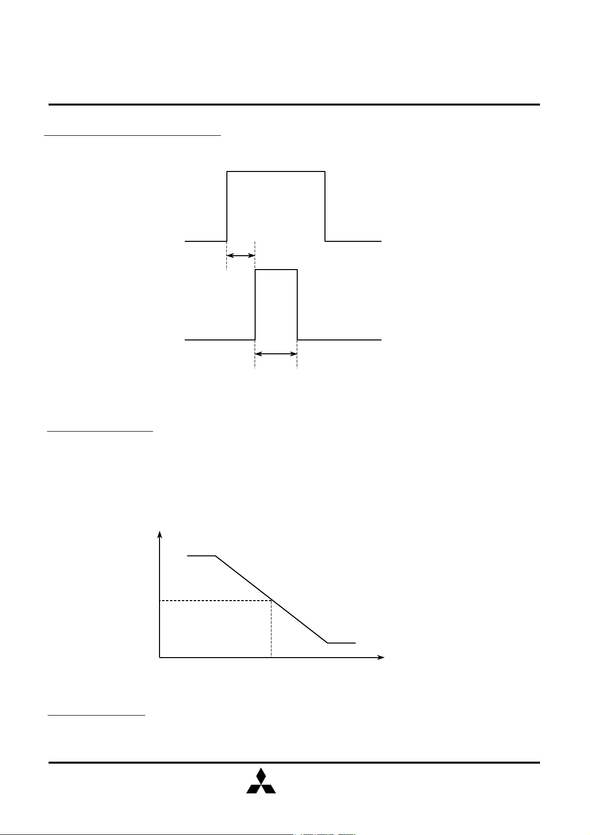
(2) VIF VCO adjustment
Before measurement of M61203CFP, VIF VCO must be adjusted by the following procedure.
(1) Input I2C bus data of VIF Freq (01H D6), according as IF frequency.
(45.75MHz : 0, 58.75MHz : 1)
(2) Input I2C bus data of VIF Defeat ON (07H D7 = 1).
(3) Set the DC voltage at pin 60 (AFT OUT) to 2.5V by adjusting I2C bus data of VCO control (01H D0-D5).
(4) Input I2C bus data of VIF Defeat OFF (07H D7 = 0).
Voltage
2.5V
45.75MHz
(or 58.75MHz)
(3) H VCO adjustment
Before measurement of M61203CFP, H VCO must be adjusted by the following procedure.
(a) Set the frequency at pin 7 (H OUT) to about 15.734kHz by adjusting I2C bus data of H VCO control
(10H D3-D5).
Frequency
MITSUBISHI
ELECTRIC
12
Page 13
MITSUBISHI ICs (TV)
M61203CFP
NTSC TV SIGNAL PROCESSOR
Electrical characteristics (Ta=25°C)
Symbol Parameter
ICC Standard conditions pin13=5V, pin27=0V
ICC23 Pins 2 and 3 supply current - - 2,3 33 41 45 mA VIF/SIF supply
Input signal
Pins SG Min. Typ. Max.
Test
point
Limits
Unit Remarks
ICC1819
ICC2324
ICC4445
ICC55 Pin 55 supply current - - 55 6 7 8 mA 8.7 VREG supply
Power
Vth13
V33H 8.7 VREG output voltage 1 - - 33 8.3 8.7 8.8 V pin13=5V
V33L 8.7 VREG output voltage 2 - - 33 - 0 0.3 V pin13=0V
V39 5.7 VREG output voltage 1 - - 39 5.45 5.6 5.85 V pin13=5V
V41H1
V41H2
V46H
V46L
Reset
Pins 18 and 19 supply
current
Pins 23 and 24 supply
current
Pins 44 and 45 supply
current
Standard conditions of
Power supply parameter
Power ON Control
threshold voltage
MCU 5.7 VREG output
voltage 1
MCU 5.7 VREG output
voltage 2
SW REG Control output
voltage 1
SW REG Control output
voltage 2
Standard conditions of
Reset parameter
- - 18,19 15 20 23 mA Start up supply Deflection
- - 23,24 35 45 50 mA VIDEO/Chroma supply
- - 44,45 10 13 15 mA RGB Drive 8V supply
pin13=5V, pin27=0V
- - 13 2.6 3 3.4 V
- - 41 5.35 5.6 5.85 V pin13=5V
- - 41 5.35 5.6 5.85 V pin13=0V
- - 46 0 0.3 1 V pin13=5V
- - 46 4.5 5 - V pin13=0V
pin13=5V
V42H Reset output high voltage - - 42 4.5 5 5.5 V
V42L Reset output low voltage - - 42 - 0 0.5 V
TH42 Reset threshold voltage - - 41 4 4.2 4.4 V
IIC
IACK ACK current - - - 1 - mA
VIL SCL/SDA input low voltage - - 5,10 0.0 0.75 1.5 V
VIH
FSCL Clock frequency - - 5 - - 100 kHz
Standard conditions of IIC
parameter
SCL/SDA input high
voltage
- - - - - - -
- - 5,10 3.5 4.25 5.0 V
MITSUBISHI
ELECTRIC
13
Page 14
MITSUBISHI ICs (TV)
M61203CFP
NTSC TV SIGNAL PROCESSOR
Symbol
ICC
ICC23
ICC1819
ICC2324
ICC4445
ICC55
Power
Vth13
V33H
V33L
V39
SUB ADDRESS
00H 01H 02H 03H 04H 05H 06H 07H 08H 09H 0AH 0BH 0CH 0DH 0EH 0FH 10H 11H 12H 13H 14H 15H 16H 17H 1BH 1CH
40 20 00 00 20 40 88 40 40 F0 80 40 40 80 80 80 24 20 00 10 00 00 00 00 00 00
40 adj 00 00 20 40 88 40 40 F0 80 40 40 80 80 80 24 20 00 10 00 00 00 00 00 00
V41H1
V41H2
V46H
V46L
Reset
V42H
V42L
TH42
IIC
IACK
VIL
VIH
40 adj 00 00 20 40 88 40 40 F0 80 40 40 80 80 80 24 20 00 10 00 00 00 00 00 00
40 adj 00 00 20 40 88 40 40 F0 80 40 40 80 80 80 24 20 00 10 00 00 00 00 00 00
FSCL
MITSUBISHI
ELECTRIC
14
Page 15
MITSUBISHI ICs (TV)
M61203CFP
NTSC TV SIGNAL PROCESSOR
Symbol Parameter
VIF
Vdc
Vo4575
Vo5875
P/N Video S/N 1,64 SG3 57 43 50 - dB
Vf
Vin min Input sensitivity 1,64 SG5 57 - 45 50 dBu
Vin max
GR AGC control range - - - 50 - - dB Vo max - Vo min
V63H Maximum IF AGC voltage - - 63 3.8 4.3 4.8 V
V63T IF AGC voltage (80dBu) 1,64 SG7 63 2.3 2.8 3.3 V
V63L Minimum IF AGC voltage 1,64 SG8 63 1.7 2.2 2.7 V
Vdefeat VIF DEFEAT function 1,64 SG1 57 0 0.1 0.2 Vpp
Standard conditions of IF
parameter
Video detector output DC
voltage
Video detector output
(45.75MHz)
Video detector output
(58.75MHz)
Video frequency
characteristics
Maximum permissible
input
Input signal
Pins SG Min. Typ. Max.
- - 57 2.2 2.7 3.2 V pin63=0V
1,64 SG1 57 0.7 1.0 1.4 Vpp
1,64 SG2 57 0.7 1.0 1.4 Vpp
1,64 SG4 57 4 5.4 - MHz
1,64 SG6 57 100 108 - dBu
Test
point
Limits
Unit Remarks
pin13=5V, pin27=0V
uAFT AFT detector sensitivity 1,64 SG9 60 7 10 13
V60H Maximum AFT voltage 1,64 SG10 60 4.2 4.7 - V
V60L Minimum AFT voltage 1,64 SG11 60 - 0.3 0.8 V
V60D AFT DEFEAT voltage - - 60 2.0 2.5 3.0 V
VCU45
VCL45
VCT45
VCU58
VCL58
VCT58
IM Intermodulation 1,64 SG13 57 - 42 - dB Reference data
DG Differential gain 1,64 SG14 57 - 3 - % Reference data
DP Differential phase 1,64 SG14 57 - 3 - deg Reference data
V62H Maximum RF AGC voltage 1,64 SG15 62 4.3 4.8 - V
V62L Minimum RF AGC voltage 1,64 SG16 62 - 0.2 0.7 V
DLPH
DLPL
Capture range (45.75MHz
upper)
Capture range (45.75MHz
lower)
Capture range (45.75MHz
total)
Capture range (58.75MHz
upper)
Capture range (58.75MHz
lower)
Capture range (58.75MHz
total)
Maximum RF AGC delay
point
Minimum RF AGC delay
point
1,64 SG9 57 1.5 2.2 - MHz Center frequency=45.75MHz
1,64 SG9 57 - -1.8 -1.1 MHz Center frequency=45.75MHz
- - 57 2.6 4.0 - MHz VCU45-VCL45
1,64 SG12 57 1.5 2.2 - MHz Center frequency=58.75MHz
1,64 SG12 57 - -1.8 -1.1 MHz Center frequency=58.75MHz
- - 57 2.6 4.0 - MHz VCU58-VCL58
1,64 SG5 62 95 108 - dBu
1,64 SG5 62 - 58 71 dBu
mV/kHz
MITSUBISHI
ELECTRIC
15
Page 16
MITSUBISHI ICs (TV)
M61203CFP
NTSC TV SIGNAL PROCESSOR
Symbol
VIF
Vdc
Vo4575
Vo5875
P/N
Vf
Vin min
Vin max
GR
V63H
V63T
V63L
Vdefeat
SUB ADDRESS
00H 01H 02H 03H 04H 05H 06H 07H 08H 09H 0AH 0BH 0CH 0DH 0EH 0FH 10H 11H 12H 13H 14H 15H 16H 17H 1BH 1CH
40 adj 00 00 20 40 88 40 40 F0 80 40 40 80 80 80 24 20 00 10 00 00 00 00 00 00
+40
uAFT
V60H
V60L
V60D
VCU45
VCL45
VCT45
VCU58
VCL58
VCT58
IM
DG
DP
V62H
V62L
DLPH
DLPL
00
7F
MITSUBISHI
ELECTRIC
16
Page 17

MITSUBISHI ICs (TV)
M61203CFP
NTSC TV SIGNAL PROCESSOR
Symbol Parameter
DLP
SPN Sync ratio 1,64 SG14 57 25 28 33 %
Symbol
DLP
SPN
RF AGC delay point
adjustment range
00H 01H 02H 03H 04H 05H 06H 07H 08H 09H 0AH 0BH 0CH 0DH 0EH 0FH 10H 11H 12H 13H 14H 15H 16H 17H 1BH 1CH
00-
7F
Input signal
Pins SG Min. Typ. Max.
- - - 33 43 - dBu DLPH-DLPL
Test
point
SUB ADDRESS
Limits
Unit Remarks
MITSUBISHI
ELECTRIC
17
Page 18

MITSUBISHI ICs (TV)
M61203CFP
NTSC TV SIGNAL PROCESSOR
Symbol Parameter
SIF
VAF
VoAF AF direct output voltage 47 SG17 53 330 590 850 mVrms
THD AF AF output distortion 47 SG17 53 - 0.5 3 %
LIM Input limiting sensitivity 47 SG17 53 - 46 55 dBu
AMR AM rejection 47 SG18 53 48 54 - dB
AFSN AF S/N 47 SG19 50 49 55 - dB
GEAu EXT Audio gain 52 SG20 50 -4.1 -2.1 -0.1 dB
SCFU
SCFL
VOL-max
VOL-min
QIF/FM
Standard conditions of SIF
parameter
AF direct output DC
voltage
SIF capture frequency
(upper)
SIF capture frequency
(lower)
Audio output maximum
amplitude
Audio ATT maximum
attenuation
Standard conditions of QIF
parameter
Input signal
Pins SG Min. Typ. Max.
- - 53 2.2 3.0 3.8 V
47 SG21 53 5.5 7.5 - MHz Vary frequency of input signal.
47 SG21 53 - 3 4.0 MHz Vary frequency of input signal.
47 SG17 50 350 620 890 mVrms
47 SG17 50 - -80 -69 dB
Test
point
Limits
Unit Remarks
pin13=5V, pin27=0V
pin13=5V, pin27=0V
QIF1 QIF detector output 1 61 SG22 49 91 97 103 dBu vi=90dBu
QIF2 QIF detector output 2 61 SG22 49 91 97 103 dBu vi=75dBu
FM-VoAF
FM-S/N FM mode S/N 61 SG22 53 38 42 - dB
FM-OUT
FM-
RFAGC1
FM-
RFAGC2
FM-
RFAGC3
FM mode AF direct output
voltage
FM mode video detector
output
FM mode RF AGC delay 1 61 SG23 62 5 23 41 data vi=100dBu
FM mode RF AGC delay 2 61 SG23 62 73 84 95 data vi=85dBu
FM mode RF AGC delay 3 61 SG23 62 100 107 114 data vi=75dBu
61 SG23 53 330 590 850
61 SG23 57 2.2 2.7 3.2 V
mVrms
MITSUBISHI
ELECTRIC
18
Page 19

MITSUBISHI ICs (TV)
M61203CFP
NTSC TV SIGNAL PROCESSOR
Symbol
SIF
VAF
VoAF
THD AF
LIM
AMR
AFSN
GEAu
SCFU
SCFL
VOL-max
VOL-min
SUB ADDRESS
00H 01H 02H 03H 04H 05H 06H 07H 08H 09H 0AH 0BH 0CH 0DH 0EH 0FH 10H 11H 12H 13H 14H 15H 16H 17H 1BH 1CH
40 adj 00 00 20 40 88 40 40 F0 80 40 40 80 80 80 24 20 00 10 00 00 00 00 00 00
80
7F
40 7F
7F
QIF/FM
QIF1
QIF2
FM-VoAF
FM-S/N
FM-OUT
FM-
RFAGC1
FM-
RFAGC2
FM-
RFAGC3
40 adj 00 00 20 40 88 40 40 F0 80 40 40 80 80 80 24 20 00 10 00 00 00 00 00 00
C0 C0
C0 C0
C0 C0
C0 C0
C0 C0
C0 C0
C0 C0
C0 C0
MITSUBISHI
ELECTRIC
19
Page 20

MITSUBISHI ICs (TV)
M61203CFP
NTSC TV SIGNAL PROCESSOR
Symbol Parameter
VIDEO
2AGTV
2AGEV
Ymax Video maximum output 34 SG.A
GY Video gain 34 SG.A
FBY
CRF Chroma trap attenuation 34 SG.C
TRF
YDL1 Y delay time 1 34 SG.A
YDL2 Y delay time 2 34 SG.A
YDL3 Y delay time 3 34 SG.A
YDL4 Y delay time 4 34 SG.A
GTnor
GTmax
GTmin
GT2M
GT5M
BLS Black stretch characteristic 34 SG.K
VMF Video mute function 34 SG.A
Standard conditions of
video character
Video SW output level (TV
input)
Video SW output level
(External input)
Video frequency
characteristics
Chroma trap maximum
attenuation
Video tone control
characteristic 1
Video tone control
characteristic 2
Video tone control
characteristic 3
Video tone control
characteristic 4
Video tone control
characteristic 5
Input signal
Pins SG Min. Typ. Max.
- - - - - - - pin13=5V,pin27=0V
36 SG.A 40 1.6 2.0 2.6 Vpp
34 SG.A 40 1.6 2.0 2.6 Vpp
34 SG.B
34 SG.C
34 SG.B
34 SG.B
34 SG.B
34 SG.B
34 SG.B
Test
point
14,15,
16
14,15,
16
14,15,
16
14,15,
16
14,15,
16
14,15,
16
14,15,
16
14,15,
16
14,15,
16
14,15,
16
14,15,
16
14,15,
16
14,15,
16
14,15,
16
14,15,
16
14,15,
16
Limits
2.9 4.2 5.6 V
12 15 18 dB
-4 -1 - dB f=5MHz, C-trap : OFF
- - -18 dB
- - -20 dB After Trap fine adj. is adjusted.
190 260 330 nS
120 200 280 nS YDL2=measure - YDL1
120 200 280 nS YDL3=measure - YDL2
120 200 280 nS YDL4=measure - YDL3
1.0 1.4 1.8 V f=2.5MHz
7 10 14 dB f=2.5MHz
-6 -2 2 dB f=2.5MHz
-1 2 5 dB f=2MHz
-9 -5 -1 dB f=5MHz
0.01 0.03 0.05 V
- -45 -35 dB
Unit Remarks
MITSUBISHI
ELECTRIC
20
Page 21

MITSUBISHI ICs (TV)
M61203CFP
NTSC TV SIGNAL PROCESSOR
Symbol
VIDEO
2AGTV
2AGEV
Ymax
GY
FBY
CRF
TRF
YDL1
YDL2
YDL3
YDL4
SUB ADDRESS
00H 01H 02H 03H 04H 05H 06H 07H 08H 09H 0AH 0BH 0CH 0DH 0EH 0FH 10H 11H 12H 13H 14H 15H 16H 17H 1BH 1CH
40 adj 00 00 20 40 88 40 40 F0 80 40 40 80 80 80 24 20 00 10 00 00 00 00 00 00
8C
7F 8C 00
7F 8C 00
10 7F 8C 00
8C 00 02
8C 00
8C 00
8D 00
8E 00
8F 00
00-
03
GTnor
GTmax
GTmin
GT2M
GT5M
BLS
VMF
8C 00
3F 8C 00
00 8C 00
8C 00
8C 00
adj 8C 00 adj 30 C0
80 7F 8C 00
MITSUBISHI
ELECTRIC
21
Page 22

MITSUBISHI ICs (TV)
M61203CFP
NTSC TV SIGNAL PROCESSOR
Symbol Parameter
CHROMAStandard condition of
chroma parameter
CnorR
CnorB
ACC1 ACC characteristic 1 34 SG.E 62 -3 0 3 dB Veb, Vec : +6dB of typical input level
ACC2 ACC characteristic 2 34 SG.E 62 -4.5 0 1.5 dB Veb, Vec : -20dB of typical input level
OV
VikN Killer operation input level 34 SG.E 62 - -43 -35 dB Veb, Vec : variable
KillP Color residual at Killer on 34 SG.E 62 - -45 -30 dB Veb = 0mV
APCU APC pull-in range (upper) 34 SG.E 62 - -600 -300 Hz feb=fec : variable
APCL APC pull-in range (lower) 34 SG.E 62 300 600 - Hz feb=fec : variable
R/BN Demodulated output ratio 34 SG.E 62 0.40 0.57 0.80 - fec=feb+50kHz
R-YN1
R-YN2
TC1
TC2
Ffsc fsc output frequency 34 SG.C 25
Chroma standard output
(R-Y)
Chroma standard output
(B-Y)
Chroma overload
characteristic
Demodulation phase angle
1
Demodulation phase angle
2
TINT control characteristic
1
TINT control characteristic
2
Input signal
Pins SG Min. Typ. Max.
- - - - - - - pin13=5V, pin27=0V
34 SG.C 62 390 560 790 mV
34 SG.C 62 640 920 1290 mV
34 SG.E 62 -3 2 5 dB Vec = 800mV
34 SG.E 62 86 103 120 deg fec=feb+50kHz
34 SG.E 62 78 95 112 deg fec=feb+50kHz
34 SG.E 62 30 45 60 deg feb=fec+50kHz
34 SG.E 62 30 45 60 deg feb=fec+50kHz
Test
point
3.5793 3.5796 3.5799
Limits
Unit Remarks
MHz
Vfsc fsc output amplitude 34 SG.C 25 550 950 1350 mVpp
Ffscfree
Vfsc
fsc output frequency at fsc
free mode
fsc output amplitude at fsc
free mode
34 SG.C 25
34 SG.C 25 550 950 1350 mVpp
3.5790 3.5795 3.5810
MHz
MITSUBISHI
ELECTRIC
22
Page 23

MITSUBISHI ICs (TV)
M61203CFP
NTSC TV SIGNAL PROCESSOR
Symbol
CHROM
A
CnorR
CnorB
ACC1
ACC2
OV
VikN
KillP
APCU
APCL
R/BN
R-YN1
R-YN2
SUB ADDRESS
00H 01H 02H 03H 04H 05H 06H 07H 08H 09H 0AH 0BH 0CH 0DH 0EH 0FH 10H 11H 12H 13H 14H 15H 16H 17H 1BH 1CH
40 adj 00 00 20 40 88 40 40 F0 80 40 40 80 80 80 24 20 00 10 00 00 00 00 00 00
8C C0 40
8C 80 40
8C 80 40
8C 80 40
8C 80 40
8C 80 40
8C 80 40
8C 80 40
8C 80 40
8C
8C
8C 02
C0/
80
C0/
80
C0/
80
40
40
40
TC1
TC2
Ffsc
Vfsc
Ffscfree
Vfsc
8C 7F 80 40
8C 00 80 40
8C
8C
8C 20
8C 20
MITSUBISHI
ELECTRIC
23
Page 24

MITSUBISHI ICs (TV)
M61203CFP
NTSC TV SIGNAL PROCESSOR
Symbol Parameter
RGB
VBLK Output Blanking voltage 34 SG.A
GYtyp
GYmin
GYEnor
GYEmin
GYEclip
Lum nor
Lum max
Lum min
D(R)1
D(B)1
D(R)2
D(B)2
EXD(R)
EXD(G)
EXD(B)
EXD(R-G)
EXD(G-B)
EXD(B-R)
EXA(R)
EXA(G)
EXA(B)
EXA(R-G)
EXA(G-B)
EXA(B-R)
OFRG
OFBG
C(R)1
C(G)1
Standard condition of RGB
parameter
Contrast control
characteristic 1
Contrast control
characteristic 2
Contrast control
characteristic 3
Contrast control
characteristic 4
Contrast control
characteristic 5
Brightness control
characteristic 1
Brightness control
characteristic 2
Brightness control
characteristic 3
R Drive control
characteristic 1
B Drive control
characteristic 1
R Drive control
characteristic 2
B Drive control
characteristic 2
Digital OSD (R) I/O
characteristic
Digital OSD (G) I/O
characteristic
Digital OSD (B) I/O
characteristic
Digital OSD level
difference R and G
Digital OSD level
difference G and B
Digital OSD level
difference B and R
Analog OSD (R) I/O
characteristic
Analog OSD (G) I/O
characteristic
Analog OSD (B) I/O
characteristic
Analog OSD level
difference R and G
Analog OSD level
difference G and B
Analog OSD level
difference B and R
Offset voltage between R
and G
Offset voltage between B
and G
R Cut off control
characteristic 1
G Cut off control
characteristic 1
Input signal
Pins SG Min. Typ. Max.
- - - - - - - pin13=5V, pin27=0V
34 SG.B
34 SG.B
34 SG.A
34 SG.A
28,30 SG.F
34 SG.D
34 SG.D
34 SG.D
34 SG.A 14 2.0 4.0 6.0 dB
34 SG.A 14 2.0 4.0 6.0 dB
34 SG.A 16 -5.0 -3.0 -1.0 dB
34 SG.A 16 -5.0 -3.0 -1.0 dB
20,27,34SG.F,
SG.A
27,28,34SG.F,
SG.A
27,30,34SG.F,
SG.A
- - - -350 0 350 mV
- - - -350 0 350 mV
- - - -350 0 350 mV
20,27,34SG.F,
SG.A
27,28,34SG.F,
SG.A
27,30,34SG.F,
SG.A
_ _ _ -350 0 350 mV
_ _ _ -350 0 350 mV
_ _ _ -350 0 350 mV
34 SG.D 14,15 -150 0 150 mV Vy = 0.0V
34 SG.D 15,16 -150 0 150 mV Vy = 0.0V
34 SG.D 14 2.6 2.9 3.2 V Vy = 0.0V
34 SG.D 15 2.6 2.9 3.2 V Vy = 0.0V
Test
point
14,15,
16
14,15,
16
14,15,
16
14,15,
16
14,15,
16
14,15,
16
14,15,
16
14,15,
16
14,15,
16
14 1.0 1.5 2.0 Vpp Vosd = 1.0V, SW30=ON
15 1.0 1.5 2.0 Vpp Vosd = 1.0V, SW28=ON
16 1.0 1.5 2.0 Vpp Vosd = 1.0V, SW20=ON
14 1.2 2.1 3.0 Vpp Vosd = 0.7V
15 1.2 2.1 3.0 Vpp Vosd = 0.7V
16 1.2 2.1 3.0 Vpp Vosd = 0.7V
Limits
0 0.1 0.3 V
1.6 2.1 2.7 Vpp f=100kHz
- 200 300 mV f=100kHz
1.6 2.1 2.7 V pin31=2.9V
- 100 200 mV pin31=0.0V
0.50 0.65 0.80 V pin27=2.5V
1.7 2.1 2.5 V Vy = 0.0V
0.6 0.9 - V Vy = 0.0V
- -0.8 -0.5 V Vy = 0.0V
Unit Remarks
MITSUBISHI
ELECTRIC
24
Page 25

MITSUBISHI ICs (TV)
M61203CFP
NTSC TV SIGNAL PROCESSOR
Symbol
RGB
VBLK
GYtyp
GYmin
GYEnor
GYEmin
GYEclip
Lum nor
Lum max
Lum min
D(R)1
D(B)1
D(R)2
SUB ADDRESS
00H 01H 02H 03H 04H 05H 06H 07H 08H 09H 0AH 0BH 0CH 0DH 0EH 0FH 10H 11H 12H 13H 14H 15H 16H 17H 1BH 1CH
40 adj 00 00 20 40 88 40 40 F0 80 40 40 80 80 80 24 20 00 10 00 00 00 00 00 00
8C 00
8C 00
00 8C 00
8C 00
8C 00
00 8C 00
8C 00
8C 00 FF
8C 00 00
8C 00 00 7F
8C 00 00 7F
8C 00 00 00
D(B)2
EXD(R)
EXD(G)
EXD(B)
EXD(R-G)
EXD(G-B)
EXD(B-R)
EXA(R)
EXA(G)
EXA(B)
EXA(R-G)
EXA(G-B)
EXA(B-R)
OFRG
OFBG
8C 00 00 00
8C 00
8C 00
8C 00
8C
8C
8C
40 8C 00 10
40 8C 00 10
40 8C 00 10
8C 10
8C 10
8C 10
8C 00
8C 00
C(R)1
C(G)1
8C 00 FF
8C 00 FF
MITSUBISHI
ELECTRIC
25
Page 26

MITSUBISHI ICs (TV)
M61203CFP
NTSC TV SIGNAL PROCESSOR
Symbol Parameter
C(B)1
C(R)2
C(G)2
C(B)2
Ccon 1
Ccon 2
Ccon 3
MTXRB Matrix ratio R/B 34 SG.G 14,16 0.81 0.98 1.08 -
MTXGB Matrix ratio G/B 34 SG.G 15,16 0.29 0.37 0.45 -
DOSD1
DOSD2
AOSD1
AOSD2
B Cut off control
characteristic 1
R Cut off control
characteristic 2
G Cut off control
characteristic 2
B Cut off control
characteristic 2
Color control characteristic
1
Color control characteristic
2
Color control characteristic
3
Digital OSD speed
characteristic 1
Digital OSD speed
characteristic 2
Analog OSD speed
characteristic 1
Analog OSD speed
characteristic 2
Input signal
Pins SG Min. Typ. Max.
34 SG.D 16 2.6 2.9 3.2 V Vy = 0.0V
34 SG.D 14 1.1 1.4 1.7 V Vy = 0.0V
34 SG.D 15 1.1 1.4 1.7 V Vy = 0.0V
34 SG.D 16 1.1 1.4 1.7 V Vy = 0.0V
34 SG.C 15 2 5 8 dB
34 SG.C 15 - -15 -10 dB
34 SG.C 15 - -40 -35 dB
27,30,34SG.F,
SG.A
27,30,34SG.F,
SG.A
27,30,34SG.F,
SG.A
27,30,34SG.F,
SG.A
Test
point
14 - 0.05 0.13 us Vosd = 1.0V, SW30=ON
14 - 0.05 0.13 us Vosd = 1.0V, SW30=ON
14 - 0.05 0.13 us Vosd = 1.0V
14 - 0.05 0.13 us Vosd = 1.0V
Limits
Unit Remarks
BB(R) Blue back function (R) 34 SG.A 14 1.7 2.1 2.5 V
BB(G) Blue back function (G) 34 SG.A 15 1.7 2.1 2.5 V
BB(B) Blue back function (B) 34 SG.A 16 2.7 3.7 4.7 V
WB White raster function 34 SG.A
14,15,
16
2.7 3.7 4.7 V
MITSUBISHI
ELECTRIC
26
Page 27

MITSUBISHI ICs (TV)
M61203CFP
NTSC TV SIGNAL PROCESSOR
Symbol
C(B)1
C(R)2
C(G)2
C(B)2
Ccon 1
Ccon 2
Ccon 3
MTXRB
MTXGB
DOSD1
DOSD2
AOSD1
SUB ADDRESS
00H 01H 02H 03H 04H 05H 06H 07H 08H 09H 0AH 0BH 0CH 0DH 0EH 0FH 10H 11H 12H 13H 14H 15H 16H 17H 1BH 1CH
8C 00 FF
8C 00 00
8C 00 00
8C 00 00
80 8C 7F
80 8C 01
80 8C 00
8C
8C
7F 8C
7F 8C
7F 8C 10
AOSD2
BB(R)
BB(G)
BB(B)
WB
7F 8C 10
8C 80
8C 80
8C 80
8C A0
MITSUBISHI
ELECTRIC
27
Page 28

MITSUBISHI ICs (TV)
M61203CFP
NTSC TV SIGNAL PROCESSOR
Symbol Parameter
DEF
fH1
fH2
fH3
Hfree
FPHU
FPHL
HPT1 Horizontal pulse timing 1 34 SG.A 7 9.5 11.0 12.5 us
HPT2 Horizontal pulse timing 2 34 SG.A 7 4.5 6.0 7.5 us
HPTW Horizontal pulse width - - 7 21 25 29 us
VH Horizontal pulse amplitude - - 7 4.7 5.4 - V
HSTO
Standard condition of
defrection parameter
Horizontal free-running
frequency 1
Horizontal free-running
frequency 2
Horizontal free-running
frequency 3
Forced horizontal freerunning function
Horizontal pull-in range
(upper)
Horizontal pull-in range
(lower)
Horizontal pulse stop
function
Input signal
Pins SG Min. Typ. Max.
- - - - - - - pin13=5V, pin27=0V
- - 7 15.3 15.7 16.1 kHz
- - 7 14.7 15.1 15.5 kHz
- - 7 15.8 16.2 16.6 kHz
34 SG.A 7 15.3 15.7 16.1 kHz
34 SG.H 7 250 500 - Hz Vary frequency of input signal.
34 SG.H 7 - -500 -250 Hz Vary frequency of input signal.
- - 7 - 0.0 0.5 V
Test
point
Limits
Unit Remarks
AFCG AFC gain operation 34 SG.A 11 2.0 3.0 10.0 dB
fV
Vfree
SVC Service mode function - - 17 4.2 4.7 5.2 V
FPVU
FPVL
VRsi 1 Vertical ramp size 34 SG.A 17 1.6 2.0 2.4 Vpp
VRsc 1
VRsc 2
VRpo 1
VRpo 2
VW Vertical pulse width 34 SG.A 29 0.35 0.53 0.65 ms
VBLKW Vertical blanking width 34 SG.A
WVSS
Vertical free-running
frequency
Forced Vertical free-run
function
Vertical pull-in frequency
(upper)
Vertical pull-in frequency
(lower)
Vertical ramp size control
range 1
Vertical ramp size control
range 2
Vertical ramp position
control range 1
Vertical ramp position
control range 2
Minimum vertical sync
detection width
- - 17 55 60 65 Hz
34 SG.A 17 55 60 65 Hz
34 SG.H 17 63 67 - Hz Vary frequency of input signal.
34 SG.H 17 - 55 57 Hz Vary frequency of input signal.
34 SG.A 17 2.0 2.4 2.8 Vpp
34 SG.A 17 0.8 1.2 1.6 Vpp
34 SG.A 17 18 38 58 us
34 SG.A 17 840 860 880 us (Measured value) - (Vrpo 1)
14,15,
34 SG.I 17 13 - - us Vary duty cycle of input signal.
1.32 1.47 1.62 ms
16
MITSUBISHI
ELECTRIC
28
Page 29

MITSUBISHI ICs (TV)
M61203CFP
NTSC TV SIGNAL PROCESSOR
Symbol
DEF
fH1
fH2
fH3
Hfree
FPHU
FPHL
HPT1
HPT2
HPTW
VH
HSTO
SUB ADDRESS
00H 01H 02H 03H 04H 05H 06H 07H 08H 09H 0AH 0BH 0CH 0DH 0EH 0FH 10H 11H 12H 13H 14H 15H 16H 17H 1BH 1CH
40 adj 00 00 20 40 88 40 40 F0 80 40 40 80 80 80 24 20 00 10 00 00 00 00 00 00
04
34
8C 90
8C
8C
8C 08 30
8C F8 30
AFCG
fV
Vfree
SVC
FPVU
FPVL
VRsi 1
VRsc 1
VRsc 2
VRpo 1
VRpo 2
VW
VBLKW
8C 30
8C C0
18
8C
8C
8C
8C 30
8C 00
8C
8C 17
8C
8C 00
WVSS
8C
MITSUBISHI
ELECTRIC
29
Page 30

MITSUBISHI ICs (TV)
MONIT
ORING
M61203CFP
NTSC TV SIGNAL PROCESSOR
Symbol Parameter
Standard condition of
Intelligent monitor
MONI1
MONI2-1
MONI2-2
MONI3
MONI4
MONI5
MONI6
MONI7
MONI8
MONI9
MONI10
MONI11
MONI12
MONI13
MONI14
MONI15
Intelligent monitoring 1
(AFT)
Intelligent monitoring 2-1
(RF AGC1)
Intelligent monitoring 2-2
(RF AGC2)
Intelligent monitoring 3
(Audio direct out)
Intelligent monitoring 4
(Audio bypass)
Intelligent monitoring 5
(Video SW output)
Intelligent monitoring 6
(G out)
Intelligent monitoring 7
(R out)
Intelligent monitoring 8
(B out)
Intelligent monitoring 9
(ACL)
Intelligent monitoring 10
(Composit sync)
Intelligent monitoring 11
(H out)
Intelligent monitoring 12
(VIF Vcc)
Intelligent monitoring 13
(Start-up Vcc)
Intelligent monitoring 14
(Video/chroma Vcc)
Intelligent monitoring 15
(Hi Vcc)
Input signal
Pins SG Min. Typ. Max.
- - - - - - - pin13=5V, pin27=0V
64,1 SG.7 43 2.0 2.5 3.0 V At which AFT voltage is 2.5V
- - 43 3.75 3.95 4.15 V At which RF AGC voltage is High
64,1 SG.7 43 0.9 0.95 1.00 - pin43 voltage / pin62 voltage
47 SG.16 43 280 460 740 mVrms
47 SG.16 43 2.05 2.45 2.85 V
36 SG.A 43 0.76 0.95 1.24 Vpp
36 SG.A 43 1.5 2.0 2.5 Vpp Measure amplitude from blanking level.
36 SG.A 43 1.5 2.0 2.5 Vpp Measure amplitude from blanking level.
36 SG.A 43 1.5 2.0 2.5 Vpp Measure amplitude from blanking level.
- - 43 3.6 4.0 4.4 V
36 SG.A 43 3.2 3.6 4.0 Vpp
36 SG.A 43 2.4 2.8 3.2 Vpp
- - 43 2.35 2.50 2.65 V
- - 43 2.55 2.70 2.85 V
- - 43 2.35 2.50 2.65 V
- - 43 2.55 2.70 2.85 V
Test
point
Limits
Unit Remarks
MITSUBISHI
ELECTRIC
30
Page 31

MITSUBISHI ICs (TV)
MONIT
ORING
M61203CFP
NTSC TV SIGNAL PROCESSOR
Symbol
MONI1
MONI2-1
MONI2-2
MONI3
MONI4
MONI5
MONI6
MONI7
MONI8
MONI9
MONI10
SUB ADDRESS
00H 01H 02H 03H 04H 05H 06H 07H 08H 09H 0AH 0BH 0CH 0DH 0EH 0FH 10H 11H 12H 13H 14H 15H 16H 17H 1BH 1CH
40 adj 00 00 20 40 88 40 40 F0 80 40 40 80 80 80 24 20 00 10 00 00 00 00 00 00
10
20
20
30
40
50
00 60
00 70
00 80
90
A0
MONI11
MONI12
MONI13
MONI14
MONI15
B0
C0
D0
E0
F0
MITSUBISHI
ELECTRIC
31
Page 32

Electrical characteristics test method
VIF BLOCK
P/N : Video S/N
1. Input SG3 and measure the rms value of output signal at
pin 57.
2. P/N is defined as follows:
P/N = 20 log
Vf : Video frequency characteristics
1. Input SG4 and set the frequency f2 to 44.75MHz so that
the beat element of 1MHz is output to pin 57.
2. Then set the applied voltage at pin 63 so that the beat
element of 1MHz at pin 64 may be 100dBµ.
3. Decrease f2 to the level at which the beat element
becomes 3dB smaller than the element of 1MHz, and read
the value at that level.
pin 57
1MHz
Vin min : Input sensitivity
1. Decrease SG5 level until the video detector output is 3dB
smaller than the measured value of Parameter Vo "Video
detector output".
Vin max : Maximum permissible input
1. Input 90dBµ SG6.
2. VA is the output level at pin 57. Increase amplitude of SG6
until the output at pin 57 becomes 3dB smaller than VA. The
input level at that time is the maximum permissible input.
Vo measured value(Vp-p) X 103 X 0.7
Noise measured value(mVrms)
100dBµ
3dB
Vf
(dB)
freq
MITSUBISHI ICs (TV)
M61203CFP
NTSC TV SIGNAL PROCESSOR
SIF, QIF BLOCK
LIM : Input limiting sensitivity
Decrease the input level of SG19. Measure the input level
when the element of 400Hz at pin 57 is 3dB smaller than
VoAF P (Maximum AF output (5.5M)).
AMR : AM Rejection
1. Vam is the element of 400Hz at pin 53.
2. AMR is defined as follows:
AMR = 20 log (dB)
AFSN : AF S/N
1. Measure the noise (20Hz to 100KHz) of output at pin 50.
2. AFSN is defined as follows:
FM-SM : FM mode S/N
1. Set FM Radio and SPLIT control data to 'ON'.
2. Input SG22 (vi=85dBµ) to pins 64 and 1.
3. Measure the noise (20Hz to 100kHz) of output at pin 53.
4. FM-SN is defined as follows:
FM-SN = 20 log
FM-OUT : FM mode video detector output
1. Set FM Radio and SPLIT control data to 'ON'.
2. Input SG23 to pins 64 and 1.
3. Measure the DC voltage of output at pin 57.
VoAF P(mVrms)
Vam(mVrms)
VoAF max
Measured value
FM-VoAF
Measured value
(dB)AF S/N = 20 log
(dB)
µAFT : AFT detector sensitivity
V2H : Maximum AFT voltage
V2L : Minimum AFT voltage
See the following figure.
pin 60
V60H
3.0V
1.0V
44.75MHz 46.75MHzf0
µAFT is defined as follows:
(3.0-1.0) X 103mV
df KHz
df
V60L
(mV/KHz)µAFT =
IM : Intermodulation
1. Input SG13 to pins 64 and 1.
2. Measure elements of 0.92MHz and 3.58MHz of output at
pin 57.
3. IM is defined as follows:
Element of 0.92MHz
Element of 3.58MHz
(dB)IM = 20 log
DLPH : Maximum RF AGC delay point
DLPL : Minimum RF AGC delay point
1. Input SG5 to pins 64 and 1.
2. Change amplitude of SG5 to the level at which voltage of
pin 62 becomes 2.5V, and read the value at that level.
freq
MITSUBISHI
ELECTRIC
32
Page 33

MITSUBISHI ICs (TV)
M61203CFP
NTSC TV SIGNAL PROCESSOR
VIDEO BLOCK
2AGTV :Video SW output level (TV input)
2AGEV :Video SW output level (External input)
1. Input SG.A to pin 36 (2AGTV) or pin 34 (2AGEV).
2. Measure the amplitude (peak to peak) at pin 40.
Note : use sub address 06H to select TV or external video
input.
Ymax : Maximum video output
1. Input SG.A to pin 34.
2. Measure the amplitude (peak to peak) except measure
from blanking part of output at pins 14, 15 and 16.
M
FBY : Video frequency characteristics
1. Input SG.B (5MHz, 0.4Vp-p) to pin 34.
2. Measure the amplitude (peak to peak) except measure
from blanking part of the output at pins 14, 15 and 16. The
amplitude is defined as YB.
3. FBY is defined as follows:
FBY = 20 log
CRF : Chroma trap attenuation (common to R/G/B output)
TRF : Chroma trap maximum attenuation
1. Input SG.C to pin 34. Measure the frequency level of
3.58MHz at trap on/off (02H D4) data 1. The level is defined
as N0.
2. Then, measure the level at trap on/off data 1 (trap active).
3. CRF is defined as follows.
CRF = 20 log
4. TRF is minimum value of CRF at which I2C bus data of
Trap fine adj. (12H D0/D1) is adjusted.
YDL1 : Y delay time 1
1. Input SGA to pin 34.
2. Measure the delay time from signal input to output at pins
14, 15 and 16.
YB Vp-p
GY Vp-p
Measured value (mVp-p)
(dB)
N0 (mVp-p)
(dB)
SGA Output signal
M
GTmax : Video tone control characteristic 1
1. Input SG.B (f=2.5MHz) to pin 34.
2. The output amplitude at pins 14, 15 and 16 when video
tone data is center (20H) are defined as GTnor.
3. Measure output amplitude at pins 14, 15 and 16 at video
tone data maximum.
4. GTmax is defined as follows:
GTmax = 20 log
Measured value (mVp-p)
GTnor (mVp-p)
(dB)
GTmin : Video tone control characteristic 2
1. Input SG.B (f=2.5MHz) to pin 34.
2. The output amplitude at pins 14, 15 and 16 when video
tone data is center (20H) are defined as GTnor.
3. Measure output amplitude at pins 14, 15 and 16 at video
tone data minimum.
4. GTmin is defined as follows:
GTmin = 20 log
Measured value (mVp-p)
GTnor (mVp-p)
(dB)
GT1M : Video tone control characteristic 3
1. The output amplitude at pins 14, 15 and 16 when
frequency of input signal is 2.5MHz are defined as GTnor.
2. Input SG.B (f=2MHz) to pin 34.
3. Measure output amplitude at pins 14, 15 and 16.
4. GT2M is defined as follows:
GT2M = 20 log
Measured value (mVp-p)
GTnor (mVp-p)
(dB)
GT5M : Video tone control characteristic 4
1. The output amplitude at pins 14, 15 and 16 when
frequency of input signal is 2.5MHz are defined as GTnor.
2. Input SG.B (f=5MHz) to pin 34.
3. Measure output amplitude at pins 14, 15 and 16.
4. GT5M is defined as follows:
GT5M = 20 log
Measured value (mVp-p)
GTnor (mVp-p)
(dB)
BLS Black stretch characteristics
1. Input SG.K to pin 34.
2. At condition of Black stretch OFF (06H D3=1), set output
level of the first step (the lowest step) to 2.0V and eighth step
(the highest step) to 4.6V at pins 14, 15 and 16 by adjusting
Contrast (05H) and Brightness (0AH).
3. Change to Black stretch ON (06H D3=0), and measure the
output level of the first step at pins 14, 15 and 16.
4. BLS is defined as follows:
BLS = 2.0 - Measured value (V)
4.6V
Black stretch OFF
Measure the delay time at the center point of rise.
YDL2, 3 and 4 : Y delay time 2, 3 and 4
1. Input SGA to pin 34.
2. Measure the delay time from signal input to output at pins
14, 15 and 16.
3. YDL2, YDL3 and YDL4 are defined as follows:
YDL2=Measured value (nsec) - YDL1
YDL3=Measured value (nsec) - YDL2
YDL4=Measured value (nsec) - YDL3
VMF Video mute characteristics
1. Input SG.A to pin 34.
2. Measure output amplitude when mute switch (02H D7) is
on "VMFon" and off "VMFoff".
3. VMF is defined as follows:
VMF = 20 log
MITSUBISHI
ELECTRIC
2.0V
Black stretch ON
M
VMFon (Vp-p)
VMFoff (Vp-p)
0V
(dB)
33
Page 34

MITSUBISHI ICs (TV)
-
1
-
1 (B/A)
M61203CFP
NTSC TV SIGNAL PROCESSOR
CHROMA BLOCK
CnorR : Standard chroma output (R-Y)
CnorB : Standard chroma output (B-Y)
1. Input SG.C to pin 34.
2. CnorR and CnorB are output amplitude measured at pin 62
when I2C data of 'test mode' 16H D6=1, D7=1 and D6=0,
D7=1 respectively.
ACC1: ACC characteristics 1
1. Input SG.E (eb=570mV:level+6dB) to pin 34.
2. Measure the output amplitude at pin 62.
3. ACC1 is defined as follows:
ACC1 = 20 log
ACC2 : ACC characteristics 2
1. Input SG.E (input level:-20dB) to pin 34.
2. Measure the output amplitude at pin 62.
3. ACC2 is defined as follows:
ACC2 = 20 log
OV : Chroma overload characteristics
1. Input SG.E (ec=800mVp-p:chroma+3dB) to pin 34.
2. Measure the output amplitude at pin 62.
3. OV is defined as follows:
OV = 20 log
VikN1 : Killer operating input level 1
VikN2 : Killer operating input level 2
1. Input SG.E (level:variable) to pin 34 at input level 0dB.
2. Lower the input level while monitoring the output amplitude
at pin 62, and measure the input level when output amplitude
is not found.
Measured value (mVp-p)
Cnor1 (mVp-p)
Measured value (mVp-p)
Cnor1 (mVp-p)
Measured value (mVp-p)
Cnor1 (mVp-p)
(dB)
(dB)
(dB)
R-YN : Demodulated phase angle
1. Input SG.E (eb=single chroma=ec+50KHz) to pin 34.
2. VRY is the output amplitude at pin 62 when I2C bus data of
'test mode' 16H D6=1, D7=1 .
3. VBY is the output amplitude at pin 62 when I2C bus data of
'test mode' 16H D6=0, D7=1 .
4. R-YN is defined as follows:
R-YN = Tan
Note: Vector should be found with taking the gain ratio of a
demodulator into consideration.
VRY X 3.8
(VBY X 1.9)+45
(deg)
TC1 : Tint control characteristics 1
TC2 : Tint control characteristics 2
1. Input SG.C (see the following figure) to pin 34. Based on
the output voltage at pin 62, find the absolute angle as shown
in the above figure.
-180deg 0deg 90deg
A
B
GND
2. Tint data center (07H data 40H) is defined as the reference
angle "TC". Find angles at tint data maximum and tint data
minimum. TC1 and TC2 are differences in angle between
TCmax and TC and between TCmin and TC and defined as
follows.
TC1 = TCmax - TC (deg)
TC2 = TC - TCmin (deg)
90deg
q
B
q =Tan
A
0deg
KillP : Killer color residual
1. Input SG.E (level:-40dB) to pin 34.
2. Measure the output amplitude at pin 62.
APCU : APC pull-in range (Upper)
APCL : APC pull-in range (Lower)
1. Input SG.E (feb=fec=3.579545MHz) to pin 34.
2. Increase the frequency until the output from pin 62
disappears. Decrease the frequency and note the point at
which the output reappears; fU.
3. Decrease the frequency until the output from pin 62
dissappears. Increase the frequency and note the point at
which the output reappears; fL.
4. APCU and APCL are defined as follows:
APCU = fU - 357954500 (Hz)
APCL = fL - 357954500 (Hz)
R/BN : Demodulation output ratio
1. Input SG.E (eb=single chroma=ec+50KHz) to pin 34.
2. VRY is the output amplitude at pin 62 when I2C bus data of
'test mode' 16H D6=1, D7=1 .
3. VBY is the output amplitude at pin 62 when I2C bus data of
'test mode' 16H D6=0, D7=1 .
4. R/BN is defined as follows:
R/BN =
VRY (mVp-p)
VBY (mVp-p)
MITSUBISHI
ELECTRIC
34
Page 35

RGB INTERFACE BLOCK
MITSUBISHI ICs (TV)
M61203CFP
NTSC TV SIGNAL PROCESSOR
VBLK : Output blanking voltage
1. Input SG.A to pin 34.
2. Measure the voltage of pedestal part and blanking part at
pins 14, 15 and 16.
Output waveform
VBLK
GND
GYmax : Contrast control characteristic 1
GYmin : Contrast control characteristic 2
1. Input SG.B (f=100KHz) to pin 34.
2. Measure output amplitude at pins 14, 15 and 16.
GYEnor : Contrast control characteristic 3
GYEmin : Contrast control characteristic 4
1. Input SG.A to pin 34.
2. Measure output amplitude at pins 14, 15 and 16 when 2.9V
and 0V are externally applied to pin 31.
GYEcrip : Contrast control characteristic 5
1. Input SG.F to pins 20, 27, 28 and 30.
2. Set contrast control data to minimum and measure the
output amplitude which is higher than the pedestal level at
pins 14, 15 and 16. The amplitude at blanking part should not
be measured.
Lum nor : Brightness control characteristic 1
Lum max : Brightness control characteristic 2
Lum min : Brightness control characteristic 3
1. Input SG.D (Vy=0V) to pin 34.
2. Measure DC voltage of output at pins 14, 15 and 16 except
that at blanking part.
Output waveform
M
D(R)2 : Drive control characteristic 2 (R)
1. Input SG.A to pin 34.
2. Measure DRnor and DRmin which are output amplitude at
pin 14 at Drive(R) data center and Drive(R) data minimum
respectively.
3. D(R)2 is defined as follows:
D(R)2 = 20 log
DRmin (Vp-p)
DRnor (Vp-p)
(dB)
D(B)2 : Drive control characteristic 2 (B)
1. Input SG.A to pin 34.
2. Measure DBnor and DBmin which are output amplitude at
pin 16 at Drive(B) data center and Drive(B) data minimum
respectively.
3. D(B)2 is defined as follows:
D(B)2 = 20 log
DBmin (Vp-p)
DBnor (Vp-p)
(dB)
EXD(R) : Digital OSD (R) I/O characteristic
EXD(G) : Digital OSD (G) I/O characteristic
EXD(B) : Digital OSD (B) I/O characteristic
1. Input SG.F (Vosd=1.0V) to pins 20, 27, 28 and 30.
2. Measure output amplitude which is higher than the
pedestal level at pins 14, 15 and 16. The amplitude at
blanking part should not be measured.
M
EXD(R-G) : Digital OSD level difference R and G
EXD(G-B) : Digital OSD level difference G and B
EXD(B-R) : Digital OSD level difference B and R
1. EXD(R-G), EXD(G-B) and EXD (B-R) are defined as
follows:
EXD(R-G) = EXD(R) - EXD(G)
EXD(G-B) = EXD(G) - EXD(B)
EXD(B-R) = EXD(B) - EXD(R)
GND
D(R)1 : Drive control characteristic 1 (R)
1. Input SG.A to pin 34.
2. Measure DRnor and DRmax which are output amplitude at
pin 14 at Drive (R) data center and Drive (R) data maximum
respectively.
3. D(R)1 is defined as follows:
D(R)1 = 20 log
DRmax (Vp-p)
DRnor (Vp-p)
(dB)
D(B)1 : Drive control characteristic 1 (B)
1. Input SG.A to pin 34.
2. Measure DBnor and DBmax which are output amplitude at
pin 16 at Drive(B) data center and Drive(B) data maximum
respectively.
3. D(B)1 is defined as follows:
D(B)1 = 20 log
DBmax (Vp-p)
DBnor (Vp-p)
(dB)
EXA(R) : Analog OSD (R) I/O characteristic
EXA(G) : Analog OSD (G) I/O characteristic
EXA(B) : Analog OSD (B) I/O characteristic
1. Input SG.F (Vosd=0.7V) to pins 20, 27, 28 and 30.
2. Measure output amplitude which is higher than the
pedestal level at pins 14, 15 and 16. The amplitude at
blanking part should not be measured.
EXA(R-G) : Analog OSD level difference R and G
EXA(G-B) : Analog OSD level difference G and B
EXA(B-R) : Analog OSD level difference B and R
1. EXA(R-G), EXA(G-B) and EXA (B-R) are defined as
follows:
EXA(R-G) = EXA(R) - EXA(G)
EXA(G-B) = EXA(G) - EXA(B)
EXA(B-R) = EXA(B) - EXA(R)
MITSUBISHI
ELECTRIC
M
35
Page 36

MITSUBISHI ICs (TV)
M61203CFP
NTSC TV SIGNAL PROCESSOR
OFEXR : Offset voltage between R and EXT(R)
OFEXG : Offset voltage between G and EXT(G)
OFEXB : Offset voltage between B and EXT(B)
1. Input SG.D (Vy=0V) to pin 34.
2. Measure DC voltage of output at pins 14, 15 and 16 except
that at blanking part.
3. The voltage when RGB output is defined as VR, VG and VB,
and the voltage when OSD output is defined as VEXR, VEXG
and VEXB.
4.OFEXR, OFEXG and OFEXB are defined as follows:
OFEXR = VR - VEXR (V)
OFEXG = VG - VEXG (V)
OFEXB = VB - VEXB (V)
Output waveform
M
GND
C(R)1 : R cutoff characteristic 1
C(G)1 : G cutoff characteristic 1
C(B)1 : B cutoff characteristic 1
C(R)2 : R cutoff characteristic 2
C(G)2 : G cutoff characteristic 2
C(B)2 : B cutoff characteristic 2
1. Input SG.D (Vy=0V) to pin 34.
2. Measure DC voltage of output at pins 14, 15 and 16 except
that at blanking part.
DOSD1 : Digital OSD speed characteristic 1
DOSD2 : Digital OSD speed characteristic 2
1. Input SG.F (Vosd=1.0V) to pins 20, 27, 28, 30.
2. Measure rise time and fall time of the signal of output at
pins 14, 15 and 16. Measurement points should be higher
than the pedestal level and blanking part should not be
measured.
M M
OSD1 OSD2
90%
10%
Output waveform at
pins 14, 15 and 16.
AOSD1 : Analog OSD speed characteristic 1
AOSD2 : Analog OSD speed characteristic 2
1. Input SG.F (Vosd=0.7V) to pins 20, 27, 28, 30.
2. Measure rise time and fall time of the signal of output at
pins 14, 15 and 16. Measurement points should be higher
than the pedestal level and blanking part should not be
measured.
M M
OSD1 OSD2
90%
10%
Output waveform at
pins 14, 15 and 16.
Ccon1 : Color control characteristic 1
Ccon2 : Color control characteristic 2
Ccon3 : Color control characteristic 3
1. Input SG.C to pin 34.
2. Measure output amplitude at pins 14, 15 and 16 when IIC
data 08H=40h, and define as Ccon0
2. Measure output amplitude at pins 14, 15 and 16 under
each condition.
3. Ccon1, Ccon2 and Ccon3 are defined as follows:
Ccon1, Ccon2 and Ccon3
= 20 log
Measured value (Vp-p)
Ccon0 (Vp-p)
(dB)
MTXRB : Matrix ratio R/B
MTXGB : Matrix ratio G/B
1. Input SG.G (rainbow color bar) to pin 34.
2. Measure output amplitude VR, VG and VB at pins 14, 15
and 16 respectively.
3. MTXRB and MTXGB are defined as follows:
MTXRB =
MTXGB =
VR (Vp-p)
VB (Vp-p)
VG (Vp-p)
VB (Vp-p)
M
BB(R) : Blue back function (R)
BB(G) : Blue back function (G)
BB(B) : Blue back function (B)
1. Input SG.A to pin 34.
2. Measure the amplitude (peak to peak) except measure
from blanking part of output at pins 14, 15 and 16.
M
WB : White raster function
1. Input SG.A to pin 34.
2. Measure the amplitude (peak to peak) except measure
from blanking part of output at pins 14, 15 and 16.
M
MITSUBISHI
ELECTRIC
36
Page 37

DEFLECTION BLOCK
MITSUBISHI ICs (TV)
M61203CFP
NTSC TV SIGNAL PROCESSOR
fH1 : Horizontal free-running frequency 1
fH2 : Horizontal free-running frequency 2
fH3 : Horizontal free-running frequency 3
Measure the output frequency at pin 7 when no signal is
input.
Hfree : Forced horizontal free-running frequency
1. Input SG.A to pin 34.
2. Set H-free control data to 'ON', and measure the output
frequency at pin 7.
FPHU : Horizontal pull-in range (upper)
FPHL : Horizontal pull-in range (lower)
1. Input SG.H to pin 34.
2. Change the frequency of SG.H, and measure the
frequency at the moment when the output signal at pin 7 and
the input signal at pin 34 are pulled in. The horizontal pull-in
range is measured by comparing with the horizontal
frequencyof video signal.
HPT1 : Horizontal pulse timing 1
pin 34 : H-sync
HPT1, HPT2, HPT3
pin 15 : H OUT
HPT2 : Horizontal pulse timing 2
HPT3 : Horizontal pulse timing 3
1. Measure the timing of horizontal pulse as same method in
HPT1.
2. HPT2 and HPT3 are defined as follows:
HPT2, HPT3 = (Measured value) - HPT1
HPTW : Horizontal pulse width
VH : Horizontal pulse amplitude
HPTW
pin 15 : H OUT
VH
Vfree : Forced vertical free-running frequency
1. Input SG.A to pin 34.
2. Set V-free control data to 'ON', and measure the output
frequency at pin 17.
SVC : Service mode function
Measure the output DC voltage at pin 17 when the service
switch is on.
FPVU : Vertical pull-in frequency (upper)
FPVL : Vertical pull-in frequency (lower)
Change the vertical frequency of SG.H and measure the
frequency when output waveform at pin 17 is pulled in.
VRsi : Vertical ramp size
VRsc1: Vertical ramp size control range 1
VRsc2 : Vertical ramp size control range 2
M
pin 17 : V-ramp
VRpo1 : Vertical ramp position control range 1
pin 34 : V-sync
VRpo1
pin 17 : V-ramp
VRpo2 : Vertical ramp position control range 2
1. Measure the timing of vertical ramp as same method in
VRpo1
2. VRpo2 is defined as follows:
VRpo2 = (Measured value) - VRpo1
VW : Vertical pulse width
pin 17 : V. PULSE
M
HSTO : Horizontal stop operation
Confirm that the horizontal output is high when the horizontal
stop switch is on.
AFCG : AFC gain operation
1. Measure AFCon which is the output amplitude of pin 19
when AFC switch is on and AFCoff which is that when the
switch is off.
2. AFCG is defined as follows:
AFCG = 20 log
AFCon (Vp-p)
AFCoff (Vp-p)
(dB)
fV : Vertical free run frequency
Measure the output frequency at pin 17 when no signal is
input.
VBLKW : Vertical BLK width
WVSS : Minimum sync detection width
Reduce the width of signal SG.I and measure the width of
input signal when the output waveform at pin 17 loses lock
with SG.I.
MITSUBISHI
ELECTRIC
GND
Output waveform at
pins 14, 15 and 16
M
GND
37
Page 38

25
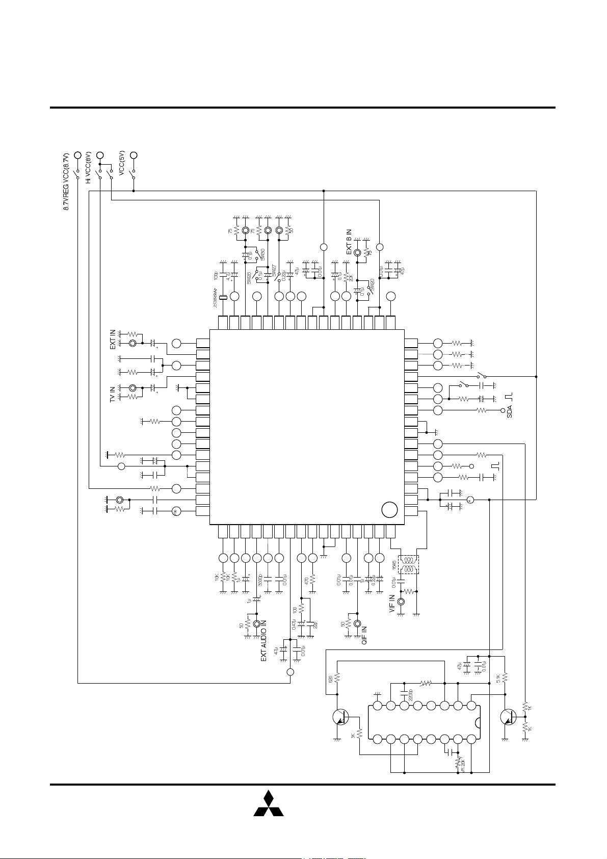
APPLICATION CIRCUIT (EVALUATION BOARD CIRCUIT)
MITSUBISHI ICs (TV)
M61203CFP
NTSC TV SIGNAL PROCESSOR
Vcc= 8V
Vcc= 5V
6.8K
2.7K
Vcc= 11V
10K
3300p
+
47u
470
0.01u
1u
0.22u
0.01u
330
SOUND TRAP
NON POLAR
1u
10K
0.47u
0.01u
49
50
OUT
AUDIO
51
BYPASS
1u
EXT AUDIO IN
52
+
FM DIRECT OUT
53
VIF VCO F/B
54
VREG Vcc
55
VIF APC FILTER
56
+
57
58
59
60
61
62
63
VIF VIDEO OUT
VIF GND(1)
VIF GND(2)
AFT OUT
QIF IN
RF AGC OUT
IF AGC FILTER 1
M61203CFP
64PIN QFP
(64P6N)
64
10K
1u
+
0.01u
2.2u
+
+
Y SW OUT
SPOT
KILLER
fsc OUT
V RAMP
FEEDBACK
100
32
31
30
3.58M X'TAL
100u
22K
100p
0.1u
29
28
27
26
24
23
22
0.22u
47u
1u
0.01u
20K
21
20
19
18
17
0.01u
47u
15u
4.5MHz
0.01u
47u
1K
1K
1u
22K
0.01u
47u
68u
0.01u
47u
MITSUBISHI
ELECTRIC
38
Page 39

MITSUBISHI ICs (TV)
5V
33K
190
190
3
5V2K2K8V8V45V6V5V
12K
8V
M61203CFP
NTSC TV SIGNAL PROCESSOR
PIN DESCRIPTION
Pin No. Name Peripheral circuit of pins DC Voltage (V)
641VIF IN (1)
VIF IN (2)
2
VIF Vcc (1)
VIF Vcc (2)
64
1.6V
1
5.0V
4
H VCO
FEEDBACK
5 SCL
3.0V
VIL : 0.75V
5
VIH : 4.25V
MITSUBISHI
ELECTRIC
39
Page 40

MITSUBISHI ICs (TV)
1008V8V
8V
8V8V8V
9
5V
5V
33K
190
100
M61203CFP
NTSC TV SIGNAL PROCESSOR
Pin No. Name Peripheral circuit of pins DC Voltage (V)
VTH : 2.0V
6 FBP IN
6
(FBP Vth L=OFF)
VTH : 1.0V
(FBP Vth L=ON)
7 H OUT
8
DEF GND (1)
DEF GND (2)
10 SDA
VOL : 0.0V
7
VOH : 5.4V
VIL : 0.75V
10
VIH : 4.25V
MITSUBISHI
ELECTRIC
40
Page 41

MITSUBISHI ICs (TV)
11
8V6V8V8V6K6K5V125V5V8V
BLK266K
8V8V8V8V8V138.7V
150K
8.7V
M61203CFP
NTSC TV SIGNAL PROCESSOR
Pin No. Name Peripheral circuit of pins DC Voltage (V)
AFC FILTER
12 FBP INV OUT
13
POWER ON
CONTROL
11
3.5V
VOL : 0.0V
VOH : 5.0V
VTH : 3.0V
14
15
16
R OUT
G OUT
B OUT
MITSUBISHI
ELECTRIC
14
15
16
41
Page 42

MITSUBISHI ICs (TV)
19
20
8V5V5V5V5V5V5V
5V178V
100
8V
8V8V8V8V8V8V8V8V8V
8V
M61203CFP
NTSC TV SIGNAL PROCESSOR
Pin No. Name Peripheral circuit of pins DC Voltage (V)
17 V OUT
START UP
18
Vcc (1)
START UP
Vcc (2)
B IN
20
4.6V
(1)Digital OSD
VIL : 0.0V
VIH : 1.0V
(2)Analog OSD
0.7Vpp
21
22
V RAMP
FEED BACK
V RAMP
CAP
MITSUBISHI
ELECTRIC
22
21
42
Page 43

MITSUBISHI ICs (TV)
24
8V8V8V
1008V5V5V8V15BLK266K
8V8V8V
8V
M61203CFP
NTSC TV SIGNAL PROCESSOR
Pin No. Name Peripheral circuit of pins DC Voltage (V)
23
Vcc (1)
Video/Chroma
Vcc (2)
25 fsc OUT
Video/Chroma
25
5.0V
3.0V
26
SPOT KILLER
27 FAST BLK
MITSUBISHI
ELECTRIC
27
14
16
7.1V
0.0-0.5V: INT RGB
1.5-3.0V: EXT RGB
4.0-5.0V: BLK
43
Page 44

MITSUBISHI ICs (TV)
8V5V5V
5V288V5V5V5V5V5V5V
5V
8V5V5V5V5V5V5V
5V
5V5V8V
M61203CFP
NTSC TV SIGNAL PROCESSOR
Pin No. Name Peripheral circuit of pins DC Voltage (V)
(1)Digital OSD
VIL : 0.0V
28 R IN
VIH : 1.0V
(2)Analog OSD
0.7Vpp
29
V PULSE
OUT
30 R IN
31
ACL/ABCL
30
29
VOL : 0.0V
VOH : 5.0V
(1)Digital OSD
VIL : 0.0V
VIH : 1.0V
(2)Analog OSD
0.7Vpp
31
MITSUBISHI
ELECTRIC
44
Page 45

MITSUBISHI ICs (TV)
970
1008V5V
5V
34
1005V5V5V5V5V8V354.3K8V5V5V5V5V5V
M61203CFP
NTSC TV SIGNAL PROCESSOR
Pin No. Name Peripheral circuit of pins DC Voltage (V)
32
32
X-TAL
3.3V
55
33
35
8.7 VREG
OUT
EXT /C IN
CHROMA
APC FILTER
33
8.7V
1.7V
34
3.2V
MITSUBISHI
ELECTRIC
45
Page 46

MITSUBISHI ICs (TV)
38
100
5V5V5V5V5V
8V
5.7V8V8V8V
8.7
V4028KVDD5V8V8V8V
M61203CFP
NTSC TV SIGNAL PROCESSOR
Pin No. Name Peripheral circuit of pins DC Voltage (V)
36
37
39
TV/Y IN
Video/Chroma
GND(1)
Video/Chroma
GND (2)
5.7 VREG
OUT
39
1.7V
36
0.0V
5.7V
40
Y SW OUT
MITSUBISHI
ELECTRIC
1.7V
46
Page 47

MITSUBISHI ICs (TV)
1.25V
8.7V8.7V8.7V8.7
V425.7V5.7V5.7
V
8.7
V
5V5V8V
M61203CFP
NTSC TV SIGNAL PROCESSOR
Pin No. Name Peripheral circuit of pins DC Voltage (V)
41
42
43
MCU 5.7VREG
OUT
MCU RESET
INTELLIGENT
MONITOR
43
41
5.7V
H: 5.0V
L: 0.0V
4445Hi Vcc (1)
Hi Vcc (2)
MITSUBISHI
ELECTRIC
8V
47
Page 48

MITSUBISHI ICs (TV)
46
49
10K
10K468.7V8.7
V
8.7
V4020p
5K5K5V5V8V
2.5K
5V5V5V5V5V5V5V8V8V
14K
5V5V8V
M61203CFP
NTSC TV SIGNAL PROCESSOR
Pin No. Name Peripheral circuit of pins DC Voltage (V)
SWITCHING
47
48
REG
CONTROL
LIMITER IN
IF AGC
FILTER 2
47
Open Collector
2.5V
48
2.3V
QIF OUT
MITSUBISHI
ELECTRIC
63
2.3V
49
48
Page 49

MITSUBISHI ICs (TV)
52
28K
8V8V8V8V8V
8V
8V5153.7K
53.7K
10.5K
10.5K
1005V5V5V8V5325K
200
5V8V8V5233K8V8V8V8V
M61203CFP
NTSC TV SIGNAL PROCESSOR
Pin No. Name Peripheral circuit of pins DC Voltage (V)
50
51
AUDIO OUT
AUDIO
BYPASS
EXT AUDIO
IN
2.3V
50
2.3V
2.3V
53
FM DIRECT
OUT
MITSUBISHI
ELECTRIC
2.3V
49
Page 50

MITSUBISHI ICs (TV)
54
5V5V5V
5V
10K
5V5V8V
55
56
12K5V5V5V8V
5V575V5V8V
M61203CFP
NTSC TV SIGNAL PROCESSOR
Pin No. Name Peripheral circuit of pins DC Voltage (V)
VIF VCO
FEEDBACK
VREG Vcc
VIF APC
FILTER
3.0V
54
8.7V
3.0V
56
57 VIDEO OUT
MITSUBISHI
ELECTRIC
2.7V
50
Page 51

MITSUBISHI ICs (TV)
1K5V5V5V5V
8V
1.5K
1.5K5V5V5V8V8V625V5V5V
8V
2.5K
5V5V5V5V5V5V5V8V8V
M61203CFP
NTSC TV SIGNAL PROCESSOR
Pin No. Name Peripheral circuit of pins DC Voltage (V)
5859VIF GND (1)
VIF GND (2)
60
61
62
AFT OUT
QIF IN
RF AGC OUT
61
60
0.3 ~ 4.7V
2.7V
0.3 ~ 4.7V
63
IF AGC
FILTER 1
MITSUBISHI
ELECTRIC
48
2.3V
63
51
 Loading...