

Page 1
MITSUBISHI <LINEAR ICS>
M61083FP
PREAMPLIFIER WITH PHOTODETECTOR FOR OPTICAL PICKUP
MITSUBISHI
ELECTRIC
( / 5 )
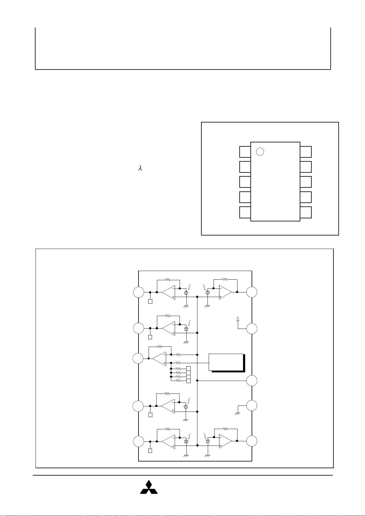
DESCRIPTION
1
12345109876DOUT
AOUT
BOUT
COUT
FOUT
VccVcGND
EOUT
Outline 10C2F
RFOUT
7
Vcc98
Vc
3
RFOUT
DOUT
1
D
2
A
5
C
4
B
F
6
EOUT
E
1.4V
power supply
The M61083FP is a semiconductor integrated circuit developed for CD-ROM (48 times speed) .
The IC is housed in a 10-pin clear molded plastic package and contains 6 preamplifiers with
divided photodetectors.
FEATURES
• Built-in 6 divided photodetectors and RF amplifiers
PIN CONFIGURATION
• Using small package (5.0 X 4.0 X 1.5mm)
• For three beam technique
• High Band preamplifier circuit (DC-65MHz)
• For infrared laser diode (ex. =780 nm)
APPLIICATION
CD-ROM etc.
RECOMMENDED OPERATING CONDITIONS
Supply voltage range • • • • • • • • • • 4.5V to 5.5V
Rated supply voltage • • • • • • • • • • 5.0V
BLOCK DIAGRAM
AOUT
BOUT
10
FOUT
D
A
A
B
C
D
GND
B
COUT
C
Page 2
MITSUBISHI <LINEAR ICS>
M61083FP
PREAMPLIFIER WITH PHOTODETECTOR FOR OPTICAL PICKUP
MITSUBISHI
ELECTRIC
( / 5 )
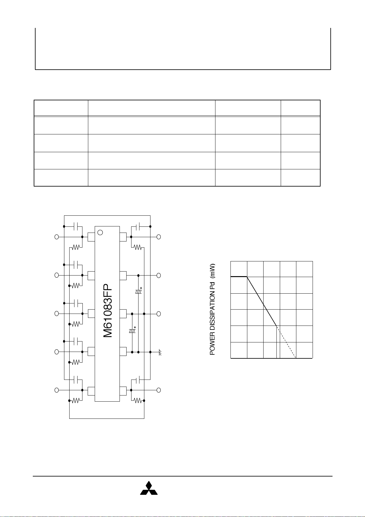
(MAXIMUM RATINGS)
AMBIENT TEMPERATURE Ta (°C)
ABSOLUTE MAXIMUM RATINGS (Ta=25°C , unless otherwise noted)
Symbol
Vcc
Pd
Topr
Tstg
Supply voltage
Power dissipation (Ta ≤ 25°C)
Operating temperature
Storage temperature
Parameter
Rating
Unit
6.0
250
-20 to +70
-40 to +100
V
mW
°C
0.22µ
0.22µ
AOUT
RFOUT
BOUT
COUT
FOUT
Vc
EOUT
Vcc
GND
10K1p10K1p10K1p10K1p10K1p10K
1p
050100
150
200
250255075100
125
70
1p
10K
10
2938475
6
°C
DOUT
1
THERMAL DERATING
300
0
Units Resistance : Ω
Capacitance : F
*Please set the condenser connected to Vcc and Vc near the pin. (Within 10mm)
2
Page 3

MITSUBISHI <LINEAR ICS>
M61083FP
PREAMPLIFIER WITH PHOTODETECTOR FOR OPTICAL PICKUP
MITSUBISHI
ELECTRIC
( / 5 )
ELECTRICAL CHARACTERISTIC (Vcc=5.0V , Vc=2.5V , Ta=25°C , unless otherwise noted)
Parameter
Symbol
Test condition
Min
Typ
Max
Output voltage
Vo
Po=10µW =780nm Output A to D
Po=10µW =780nm Output E to F
412
534
Limits
mAmVmV
offset voltage
characteristic
In the dark (A+C) - (B+D)
In the dark E-F
output A to D (at f=30MHz)
0
+15
-200+20
-200+20
-150+15–1.0
3.5
––-83
-77mVMHz
NOVOFF
6.8
9.0
11.2
2.08
times
176
292
1.51mVtimes
50
65
OFF
Output offset voltage 1
In the dark output RF
OFF
characteristic
Output A to D (f=1 to 30MHz)
42nS
-550+55
1.70
1.85
1.55
1.25
1.40
1.55
DR
OFF
The ratio of output E to F toward output
A to D
0
+20
3dB down Output E to F
50
65
5
2
-74
-66
Unit
Circuit current
Output voltage ratio 1
Output voltage ratio 2
Output offset voltage 2
Output offset
total voltage
Delta output
Icc
In the dark
232
303
VOE/VOA 1.77
VOE/VOA
The ratio of output RF toward output A to D
V
In the dark output A to F
V
In the dark total output A to D
In the dark A-B
In the dark C-D
-15
-20
∆V
V
mV
Po=10µW =780nm
3dB down Output A to D
Frequency
Group delay
Output noise voltage
fc
G
V
Po=10µW =780nm
3dB down Output RF
Po=10µW =780nm
Po=10µW =780nm
Po=10µW =780nm
Output RF (f=1 to 30MHz)
output RF (at f=30MHz)
–
–
–
3
–
dBm
Page 4

MITSUBISHI <LINEAR ICS>
M61083FP
PREAMPLIFIER WITH PHOTODETECTOR FOR OPTICAL PICKUP
MITSUBISHI
ELECTRIC
( / 5 )
PD SIZE (TYPICAL)
2345679108
ABD
C
2288124
124
56°5
ABCDF
E
66
X
3 degree
6°
22
Unit : µm
Note ) A public difference from the SPD
center and the flame
A public difference from the center of
the flame of molded package
F
1
E
A public difference from the center of
SPD and the center of molded package
The rotation deviation of SPD toward
the flame
4
+
+
+
+
0.2mm
0.2mm
0.4mm
Page 5

MITSUBISHI <LINEAR ICS>
M61083FP
PREAMPLIFIER WITH PHOTODETECTOR FOR OPTICAL PICKUP
MITSUBISHI
ELECTRIC
( / 5 )
• These materials are intended as reference to assist our customers in the selection of the Mitsubishi
Note regarding these materials
5
semiconductor product best suited to the customer's application; they do not convey any license
under any intellectual property rights, or any other rights, belonging to Mitsubishi Electric
Corporation or a third party.
• Mitsubishi Electric Corporation assumes no responsibility for any damage, or infringement of any
third-party's right,originating in the use of any product data, diagrams, charts of circuit application
examples contained in these materials.
• All information contained in these materials, including product data, diagrams and charts, represent
information on products at the time of publication of these materials, and are subject to change by
Mitsubishi Electric Corporation without notice due to product improvements or other reasons.
It is therefore recommended that customers contact Mitsubishi Electric Corporation or an
authorized Mitsubishi Semiconductor product distributor for the latest product information before
purchasing a product listed herein.
• Mitsubishi Electric Corporation semiconductors are not designed or manufactured for use in a
device or system that is used under circumstances in which human life is potentially at stake.
Please contact Mitsubishi Electric Corporation or an authorized Mitsubishi Semiconductor product
distributor when considering the use of a product contained herein for special applications, such as
apparatus or systems for transportation, vehicular, medical, aerospace, nuclear repeater use.
• The prior written approval of Mitsubishi Electric Corporation is necessary to reprint or reproduce in
whole or in part these materials.
• If these products or technologies are subject to the Japanese export control restrictions, they must
be exported under license from the Japanese government and cannot be imported into a country
other than the approved destination.
Any diversion or reexport contrary to the export control laws and regulations of Japan and/or the
country of destination is prohibited.
• Please contact Mitsubishi Electric Corporation or an authorized Mitsubishi Semiconductor product
distributor for further details on these materials or the products contained therein.
 Loading...