

Datasheet M5M5V208KR-10LL, M5M5V208KR-10L, M5M5V208FP-85LL, M5M5V208FP-85L, M5M5V208FP-70LL Datasheet (Mitsubishi)
...Page 1
'97.3.21
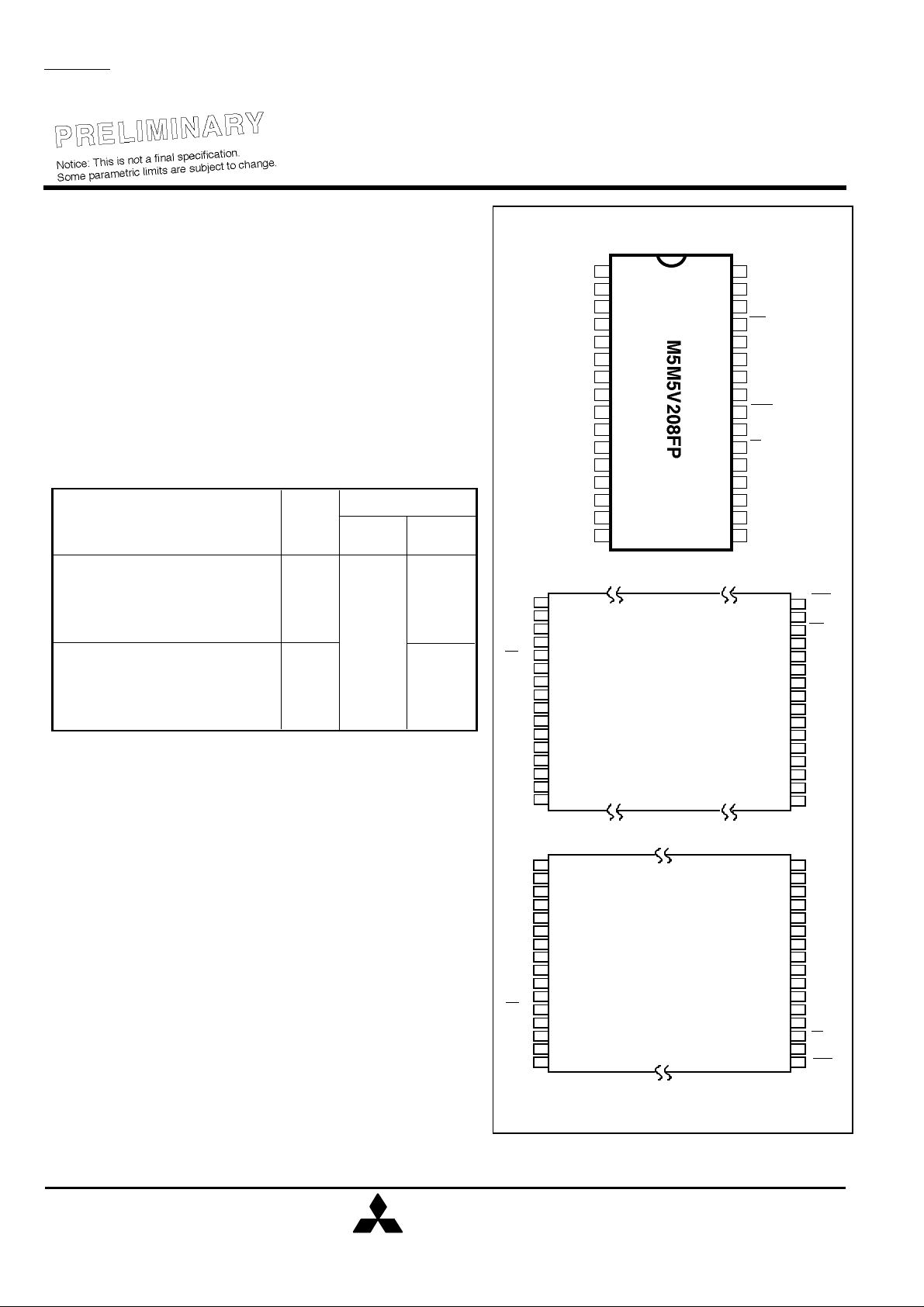
PIN CONFIGURATION (TOP VIEW)
1234567
8910111213141516
17A16A14A12
323130292827262524232221201918
17
16151413121110987654321171819202122232425262728293031
32
123456789101112131415
16
323130292827262524232221201918
17
M5M5V208FP,VP,RV,KV,KR -70L , -85L, -10L , -12L,
-70LL, -85LL, -10LL, -12LL
2097152-BIT (262144-WORD BY 8-BIT) CMOS STATIC RAM
DESCRIPTION
The M5M5V208 is 2,097,152-bit CMOS static RAM organized as
262,144-words by 8-bit which is fabricated using high-performance
quadruple-polysilicon and double metal CMOS technology. The use
of thin film transistor(TFT) load cells and CMOS periphery results in a
high density and low power static RAM. The M5M5V208 is designed
for memory applications where high reliability, large storage, simple
interfacing and battery back-up are important design objectives.
The M5M5V208VP,RV,KV,KR are packaged in a 32-pin thin small
outline package which is a high reliability and high density surface
mount device(SMD).Two types of devices are available.
VP,KV(normal lead bend type package),RV,KR(reverse lead bend
type package). Using both types of devices, it becomes very easy to
design a printed circuit board.
FEATURE
Access
Type
M5M5V208FP,VP,RV,KV,KR-70L
M5M5V208FP,VP,RV,KV,KR-85L
M5M5V208FP,VP,RV,KV,KR-10L
M5M5V208FP,VP,RV,KV,KR-12L
M5M5V208FP,VP,RV,KV,KR-70LL
M5M5V208FP,VP,RV,KV,KR-85LL
M5M5V208FP,VP,RV,KV,KR-10LL
M5M5V208FP,VP,RV,KV,KR-12LL
• Single 2.7 ~ 3.6V power supply
• Operating temperature of 0 to +70°C
• No clocks, No refresh
• All inputs and outputs are TTL compatible.
• Easy memory expansion and power down by S1 & S2
• Data retention supply voltage=2.0V
• Three-state outputs: OR-tie capability
• OE prevents data contention in the I/O bus
• Common Data I/O
• Battery backup capability
• Small stand-by current · · · · · · · · · · 0.3µA(typ.)
time
100ns
120ns
100ns
120ns
Power supply current
(max)
70ns
85ns
70ns
85ns
Active
(max)
27mA
(Vcc=3.6V)
Stand-by
(max)
60µA
(Vcc=3.6V)
10µ A
(Vcc=3.6V)
PACKAGE
M5M5V208FP : 32 pin 525 mil SOP
M5M5V208VP,RV : 32pin 8 X 20 mm2 TSOP
M5M5V208KV,KR : 32pin 8 X 13.4 mm2 TSOP
APPLICATION
Small capacity memory units
Battery operating system
Handheld communiation tools
A11
A9
A8
A13
W
S2
A15
Vcc
A17
A16
A14
A12
A7
A6
A5
A4
A4
A5
A6
A7
A12
A14
A16
A17
Vcc
A15
S2
W
A13
A8
A9
A11
A
A7
A6
A5
A4
A3
A2
A1
A0
DQ1
DQ2
DQ3
(0V)GND
Outline 32P2M-A(FP)
M5M5V208VP,KV
Outline 32P3H-E(VP), 32P3K-B(KV)
M5M5V208RV,KR
Outline 32P3H-F(RV), 32P3K-C(KR)
MITSUBISHI LSIs
VCC(3V)
A15
S2
W
A13
A8
A9
A11
OE
A10
S1
DQ8
DQ7
DQ6
DQ5
DQ4
OE
A10
S1
DQ8
DQ7
DQ6
DQ5
DQ4
GND
DQ3
DQ2
DQ1
A0
A1
A2
A3
A3
A2
A1
A0
DQ1
DQ2
DQ3
GND
DQ4
DQ5
DQ6
DQ7
DQ8
S1
A10
OE
MITSUBISHI
ELECTRIC
1
Page 2
'97.3.21
(3V)
24131415173216S12218192021
29
X 32 BLOCKS
GENERATOR
8A47A56A65A74
3
2
1
31
12A011A110A223
25
26A927A828
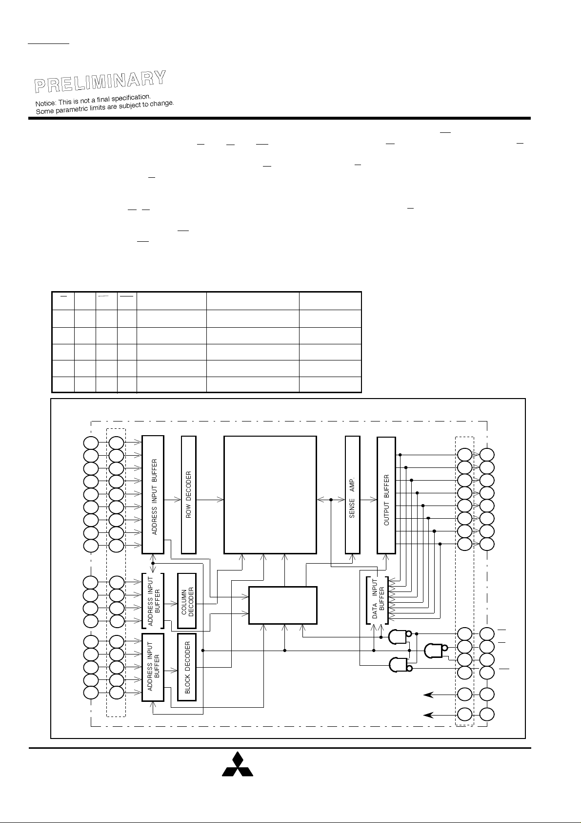
The operation mode of the M5M5V208 is determined by a
combination of the device control inputs S1, S2, W and OE.
Each mode is summarized in the function table.
A write cycle is executed whenever the low level W
overlaps with the low level S1 and the high level S2. The
address must be set up before the write cycle and must be
stable during the entire cycle. The data is latched into a cell
on the trailing edge of W, S1 or S2, whichever occurs first,
requiring the set-up and hold time relative to these edge to
be maintained. The output enable OE directly controls the
output stage. Setting the OE at a high level,the output stage
is in a high-impedance state, and the data bus contention
problem in the write cycle is eliminated.
Mode
OE
INDOUT
9
303112342019181716151413121110973282430562122232526272829
M5M5V208FP,VP,RV,KV,KR -70L , -85L, -10L , -12L,
-70LL, -85LL, -10LL, -12LL
2097152-BIT (262144-WORD BY 8-BIT) CMOS STATIC RAM
FUNCTION
A read cycle is executed by setting W at a high level and
OE at a low level while S1 and S2 are in an active state (S1
= L ,S2 = H).
When setting S1 at a high level or S2 at a low level, the
chips are in a non-selectable mode in which both reading
and writing are disabled. In this mode, the output stage is in
a high-impedance state, allowing OR-tie with other chips
and memory expansion by S1 or S2. The power supply
current is reduced as low as the stand-by current which is
specified as Icc3 or Icc4, and the memory data can be held
at +2V power supply, enabling battery back-up operation
during power failure or power-down operation in the nonselected mode.
FUNCTION TABLE
S1 W
S2
X X
LX
H
X
X X
L
L
LH
H
H
Non selection
Non selection
X
L
Write
Read
DQ Icc
High-impedance
High-impedance
D
Standby
Standby
Active
Active
MITSUBISHI LSIs
L
H
H
H
BLOCK DIAGRAM
*
A12
A14
A16
A17
A15
A3
A10
A11
A13
*Pin numbers inside dotted line show those of TSOP.
262144 WORDS
X 8 BITS
512 ROWS
X 128 COLUMNS
CLOCK
MITSUBISHI
ELECTRIC
ActiveHigh-impedance
*
DQ1
DQ2
DQ3
DQ4
DQ5
DQ6
DQ7
DQ8
W
S2
OE
VCC
GND
(0V)
2
Page 3
'97.3.21
DC ELECTRICAL CHARACTERISTICS
0 ~ Vcc
M5M5V208FP,VP,RV,KV,KR -70L , -85L, -10L , -12L,
-70LL, -85LL, -10LL, -12LL
2097152-BIT (262144-WORD BY 8-BIT) CMOS STATIC RAM
ABSOLUTE MAXIMUM RATINGS
Parameter
Vcc
VI
VO
Pd
Topr
Tstr
* –3.0V in case of AC ( Pulse width ≤ 30ns )
Supply voltage
Input voltage
Output voltage
Power dissipation
Operating temperature
Storage temperature
With respect to GND
Ta=25°C
Symbol Parameter
VIH High-level input voltage
VIL Low-level input voltage
VOH1 High-level output voltage 1 IOH= –0.5mA
VOH2 High-level output voltage 2 IOH= –0.05mA
VOL Low-level output voltage IOL=2mA
II
IO Output current in off-state
Input current VI=0 ~ Vcc
S1=VIH or S2=VIL or OE=VIH
VI/O=0 ~ Vcc
Icc1
Active supply current
(CMOS-level Input)
S1 ≤ 0.2V, S2≥ Vcc-0.2V,
other inputs ≤ 0.2V
or ≥ Vcc-0.2V,output-open
Icc2
Active supply current
(TTL-level Input)
S1=VIL,S2=VIH,
other inputs=VIH or VIL
output-open
1) S2 ≤ 0.2V or
Conditions
(Ta=0~70°C, Vcc= 2.7 ~ 3.6V, unless otherwise noted)
Test conditions
-L
– 0.5* ~ Vcc + 0.5
2.0
–0.3*
2.4
Vcc
-0.5V
f= 10MHz
f= 5MHz
f= 10MHz
f= 5MHz
-20 ~ +70°C
MITSUBISHI LSIs
RatingsSymbol
– 0.5*~4.6
(Max 4.6)
700
0 ~ 70
– 65 ~150
Limits
±1
±1
10
22
12
MaxTypMin
Vcc
+0.3V
0.6
0.4
2520
13
27
15
60
Unit
V
V
V
mW
°C
°C
Unit
V
V
V
V
V
µA
µA
mA
mA
Icc3 Stand-by current
Stand-by currentIcc4
* –3.0V in case of AC ( Pulse width ≤ 30ns )
CAPACITANCE
Symbol Parameter Test conditions
CI
CO
Note 1: Direction for current flowing into an IC is positive (no mark).
2: Typical value is for Vcc = 3V, Ta = 25°C
Input capacitance
Output capacitance
2) S1 ≥ Vcc-0.2V,
S2 ≥ Vcc-0.2V
other inputs=0 ~ Vcc
-20 ~ +70°C
-20 ~ +40°C
-LL
S1=VIH or S2=VIL,other inputs=0 ~ Vcc
(Ta=0 ~ 70°C, Vcc= 2.7 ~ 3.6V, unless otherwise noted)
VI=GND, VI=25mVrms, f=1MHz
VO=GND,VO=25mVrms, f=1MHz
MITSUBISHI
ELECTRIC
+25°C
Min
0.3
Limits
Typ
10
0.6
0.33
Max
7
9
µA
1
mA
Unit
pF
pF
3
Page 4

'97.3.21
Limits
)
) ta(OE)
)
)
(OE)
)
)
(OE)
(A) ta(A)
Limits
(W)
(A)
(A-WH)
)
)
(D) th(D)
(W)
(W)
(OE)
(W)
M5M5V208FP,VP,RV,KV,KR -70L , -85L, -10L , -12L,
-70LL, -85LL, -10LL, -12LL
2097152-BIT (262144-WORD BY 8-BIT) CMOS STATIC RAM
MITSUBISHI LSIs
AC ELECTRICAL CHARACTERISTICS
(Ta =0 ~ 70°C, Vcc= 2.7 ~ 3.6V, unless otherwise noted )
(1) MEASUREMENT CONDITIONS
Vcc 2.7 ~ 3.6V
Input pulse level VIH=2.2V,VIL=0.4V
Input rise and fall time 5ns
Reference level VOH=VOL=1.5V
Output loads Fig.1,CL=30pF
CL=5pF (for ten,tdis)
Transition is measured ±500mV from steady
state voltage. (for ten,tdis)
.................................
.............
.....
...............
...................
(2) READ CYCLE
Symbol Parameter
tCR Read cycle time
Address access time
ta(S1
ta(S2
Chip select 1 access time
Chip select 2 access time
Output enable access time
tdis(S1
tdis(S2
tdis
ten(S1
ten(S2
ten
tV
Output disable time after S1 high
Output disable time after S2 low
Output disable time after OE high
Output enable time after S1 low
Output enable time after S2 high
Output enable time after OE low
Data valid time after address
-70L,LL -85L,LL
Min
Max
70
70
70
70
35
25
25
25
10
10
5
10
Min
85
10
10
10
1TTL
DQ
CL
including
scope and JIG
Fig.1 Output load
-10L,LL
Max
100
85
85
85
45
30
30
30
100
100
100
50
35
35
35
10
10
5
5
10
-12L,LL
120
10
10
5
10
MaxMinMaxMin
120
120
120
60
40
40
40
Unit
ns
ns
ns
ns
ns
ns
ns
ns
ns
ns
ns
ns
(3) WRITE CYCLE
Symbol Parameter
tCW
tw
tsu
tsu
tsu(S1
tsu(S2
tsu
trec
tdis
tdis
ten
ten(OE)
Write cycle time
Write pulse width
Address setup time
Address setup time with respect to W
Chip select 1 setup time
Chip select 2 setup time
Data setup time
Data hold time
Write recovery time
Output disable time from W low
Output disable time from OE high
Output enable time from W high
Output enable time from OE low
Max
Min
70
55
0
65
65
65
30
0
0
25
25
5
5
MITSUBISHI
ELECTRIC
Min
85
60
70
70
70
35
-10L,LL -12L,LL-70L,LL -85L,LL
Max
Max
Min
100
75
0
0
85
85
85
40
0
0
30
30
5
5
0
0
35
35
5
5
Min
120
85
100
100
100
45
Max
0
0
0
5
5
40
40
Unit
ns
ns
ns
ns
ns
ns
ns
ns
ns
ns
ns
ns
ns
4
Page 5

'97.3.21
(S1)
(S1)
STABLE
M5M5V208FP,VP,RV,KV,KR -70L , -85L, -10L , -12L,
-70LL, -85LL, -10LL, -12LL
2097152-BIT (262144-WORD BY 8-BIT) CMOS STATIC RAM
(4) TIMING DIAGRAMS
Read cycle
A0~17
S1
ta(A)
ta (S1)
tCR
tv (A)
MITSUBISHI LSIs
(Note 3)
S2
(Note 3)
OE
(Note 3)
DQ1~8
W = "H" level
Write cycle (W control mode)
A0~17
S1
(Note 3)
ta (S2)
ta (OE)
ten (OE)
ten (S1)
ten (S2)
tsu
tCW
tdis
tdis (S2)
tdis (OE)
DATA VALID
(Note 3)
(Note 3)
(Note 3)
(Note 3)
DQ1~8
S2
OE
W
(Note 3)
tdis (OE)
tsu (S2)
tsu (A-WH)
tw (W) trec (W)tsu (A)
tdis (W)
MITSUBISHI
ELECTRIC
(Note 3)
ten(OE)
ten (W)
DATA IN
th (D)tsu (D)
5
Page 6

'97.3.21
(S1)
M5M5V208FP,VP,RV,KV,KR -70L , -85L, -10L , -12L,
-70LL, -85LL, -10LL, -12LL
2097152-BIT (262144-WORD BY 8-BIT) CMOS STATIC RAM
Write cycle ( S1 control mode)
tCW
A0~17
MITSUBISHI LSIs
S1
S2
(Note 3)
W
(Note 3)
DQ1~8
Write cycle (S2 control mode)
A0~17
tsu (A)
(Note 5)
tsu
(Note 4)
tsu (D)
DATA IN
STABLE
tCW
trec (W)
th (D)
(Note 3)
(Note 3)
S1
S2
W
DQ1~8
(Note 3)
tsu (A)
(Note 5)
(Note 3)
Note 3: Hatching indicates the state is "don't care".
4: Writing is executed while S2 high overlaps S1 and W low.
5: When the falling edge of W is simultaneously or prior to the falling edge of S1
or rising edge of S2, the outputs are maintained in the high impedance state.
6: Don't apply inverted phase signal externally when DQ pin is output mode.
tsu (S2) trec (W)
(Note 4)
tsu (D)
DATA IN
STABLE
th (D)
MITSUBISHI
ELECTRIC
(Note 3)
(Note 3)
6
Page 7

'97.3.21
(Note 7)
M5M5V208FP,VP,RV,KV,KR -70L , -85L, -10L , -12L,
-70LL, -85LL, -10LL, -12LL
2097152-BIT (262144-WORD BY 8-BIT) CMOS STATIC RAM
POWER DOWN CHARACTERISTICS
(1) ELECTRICAL CHARACTERISTICS
Symbol
Vcc (PD)
VI (S1)
VI (S2)
Icc (PD)
Note7: ICC (PD) = 0.5µA (Max.) in case of Ta = +25°C
Power down supply voltage
Chip select input S1
Chip select input S2
Power down supply current
Parameter
Test conditions Unit
Vcc = 3.0V
S2 ≤ 0.2V or
S1 ≥ Vcc - 0.2V,S2 ≥ Vcc - 0.2V
(Ta = 0 ~ 70°C, unless otherwise noted)
Min
2
2.0
-L
-LL
MITSUBISHI LSIs
Limits
MaxTyp
0.2
50
0.3
8
V
V
V
µA
(2) TIMING REQUIREMENTS
Symbol
tsu (PD)
trec (PD)
Power down set up time
Power down recovery time
Parameter
(3) POWER DOWN CHARACTERISTICS
S1 control mode
Vcc
t su (PD)
2.2V
2.7V
S1
S2 control mode
Vcc
S2
t su (PD)
2.7V
Test conditions
S1≥ Vcc - 0.2V
2.7V
2.7V
(Ta = 0 ~ 70°C, unless otherwise noted )
Min
0
5
Limits
MaxTyp
Unit
ns
ms
t rec (PD)
2.2V
t rec (PD)
0.2V
S2 ≤ 0.2V
0.2V
MITSUBISHI
ELECTRIC
7
 Loading...