

Datasheet M5M51008DVP-70H, M5M51008DVP-55H, M5M51008DRV-70H, M5M51008DRV-55H, M5M51008DKV-70H Datasheet (Mitsubishi)
...Page 1
MITSUBISHI LSIs
Ver. 1.1
MITSUBISHI
ELECTRIC
NC : NO CONNECTION
DESCRIPTION
FEATURES
Type name
Access
time
(max)
Active
(max)
stand-by
(max)
Power supply current
The M5M51008DP,FP,VP,RV,KV are a 1048576-bit CMOS static
RAM organized as 131072 word by 8-bit which are fabricated using
high-performance quadruple-polysilicon and double metal CMOS
technology. The use of thin film transistor (TFT) load cells and
CMOS periphery result in a high density and low power static
RAM.
They are low standby current and low operation current and ideal
for the battery back-up application.
The M5M51008DVP,RV,KV are packaged in a 32-pin thin small
outline package which is a high reliability and high density surface
mount device(SMD). Two types of devices are available.
M5M51008DVP(normal lead bend type package),
M5M51008DRV(reverse lead bend type package).Using both types
of devices, it becomes very easy to design a printed circuit board.
Package
APPLICATION
Small capacity memory units
Directly TTL compatible : All inputs and outputs
Easy memory expansion and power down by S1,S2
Data hold on +2V power supply
Three-state outputs : OR - tie capability
OE prevents data contention in the I/O bus
Common data I/O
M5M51008DFP,VP,RV,KV-55H
55ns
15mA
70ns
20µA
(1MHz)
M5M51008DFP,VP,RV,KV-70H
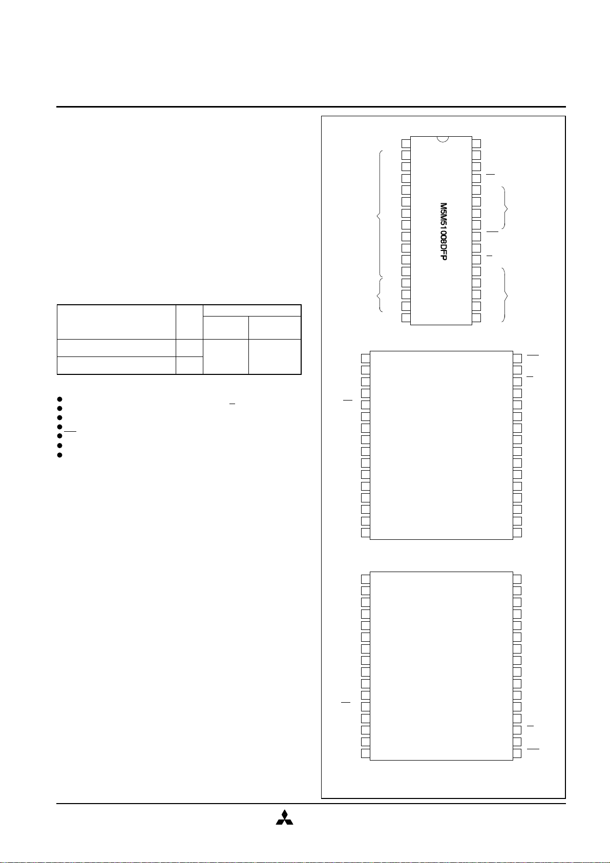
PIN CONFIGURATION (TOP VIEW)
NC
A16
A14
A12A7A6A5A4A3A2A1A0
DQ1
DQ2
DQ3
GND
VCC
A15S2W
A13A8A9
A11OEA10S1DQ8
DQ7
DQ6
DQ5
DQ4
A11A9A8
A13WS2
A15
VCCNCA16
A14
A12A7A6A5A4OEA10S1DQ8
DQ7
DQ6
DQ5
DQ4
GND
DQ3
DQ2
DQ1A0A1A2A3A4A5A6A7
A11A2A0OEA1
A3
M5M51008DVP,KV
A14
A16NCVCC
A15S2W
A13A8A9
DQ1
DQ2
DQ3
GND
DQ4
DQ5
DQ6
DQ7
DQ8S1A10
A12
32P3K-B(KV)
INPUT
INPUT
INPUT
ADDRESS
INPUTS
INPUT
INPUT
INPUT
DATA
INPUTS/
OUTPUTS
ADDRESS
INPUTS
DATA
INPUTS/
OUTPUTS
M5M51008DRV
(Vcc=5.5V)
(1MHz)
1
M5M51008DFP ············ 32pin 525mil SOP
M5M51008DVP,RV ············ 32pin 8 X 20 mm TSOP
M5M51008DKV ············ 32pin 8 X 13.4 mm TSOP
M5M51008DFP,VP,RV,KV,KR -55H, -70H
1048576-BIT(131072-WORD BY 8-BIT)CMOS STATIC RAM
1
2
3
4
5
6
7
8
9
10
11
12
13
14
15
16
32
31
30
29
28
27
26
25
24
23
22
21
20
19
18
17
ADDRESS
CHIP SELECT
WRITE CONTROL
OUTPUT ENABLE
ADDRESS
CHIP SELECT
Outline 32P2M-A(FP)
1
2
3
4
5
6
7
8
9
2
2
10
11
12
13
14
15
16
32
31
30
29
28
27
26
25
24
23
22
21
20
19
18
17
Outline 32P3H-E(VP),
16
15
14
13
12
11
10
9
8
7
6
5
4
3
2
1
Outline 32P3H-F(RV)
17
18
19
20
21
22
23
24
25
26
27
28
29
30
31
32
Page 2
MITSUBISHI LSIs
Ver. 1.1
MITSUBISHI
ELECTRIC
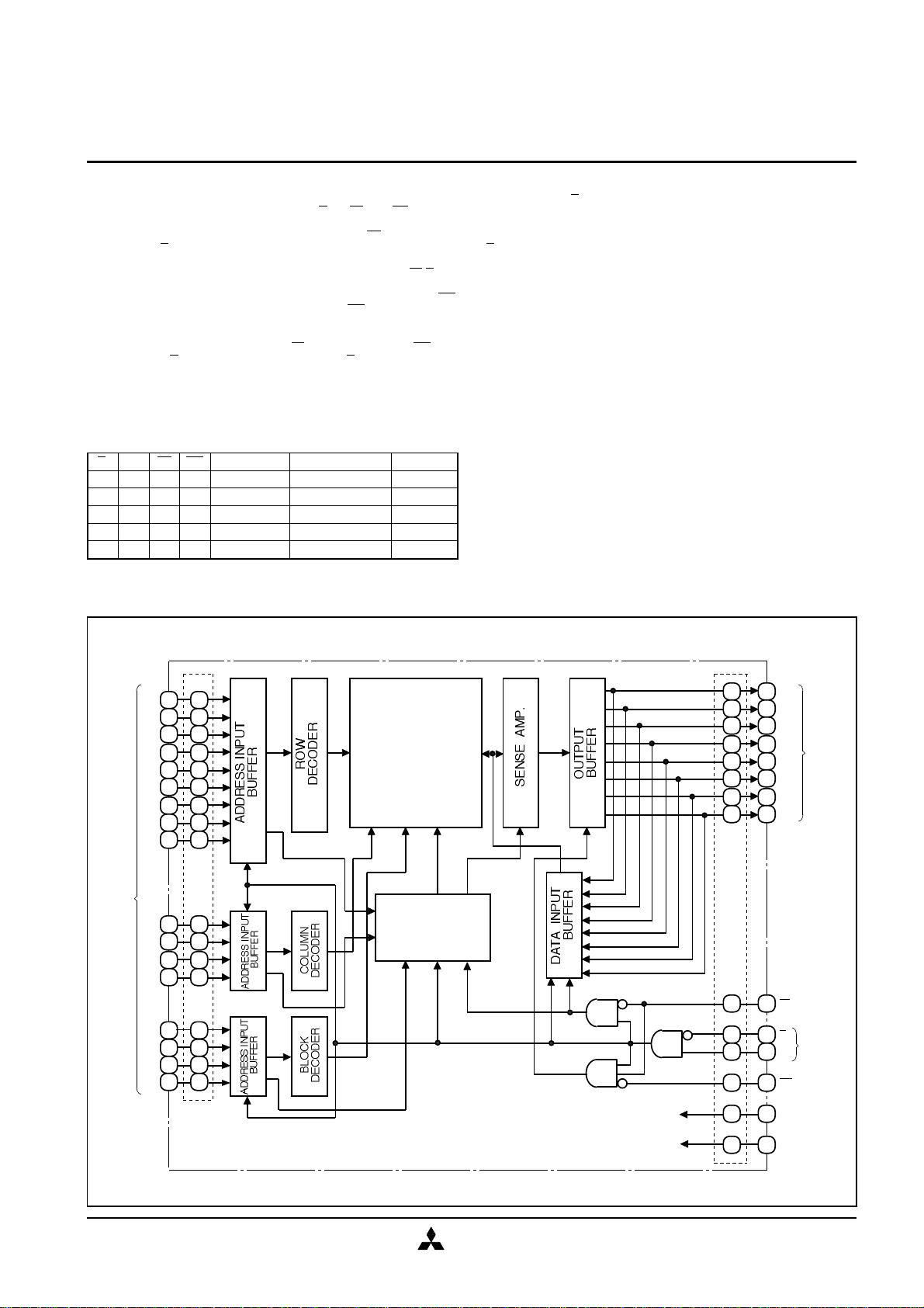
FUNCTION
BLOCK DIAGRAM
The operation mode of the M5M51008D series are determined by
a combination of the device control inputs S1,S2,W and OE.
Each mode is summarized in the function table.
A write cycle is executed whenever the low level W overlaps with
the low level S1 and the high level S2. The address must be set up
before the write cycle and must be stable during the entire cycle.
The data is latched into a cell on the trailing edge of W,S1 or
S2,whichever occurs first,requiring the set-up and hold time relative
to these edge to be maintained. The output enable input OE
directly controls the output stage. Setting the OE at a high level,
the output stage is in a high-impedance state, and the data bus
contention problem in the write cycle is eliminated.
A read cycle is executed by setting W at a high level and OE at a
low level while S1 and S2 are in an active state(S1=L,S2=H).
When setting S1 at a high level or S2 at a low level, the chip are in
a non-selectable mode in which both reading and writing are
disabled. In this mode, the output stage is in a high- impedance
state, allowing OR-tie with other chips and memory expansion by
S1 and S2. The power supply current is reduced as low as the
stand-by current which is specified as ICC3 or ICC4, and the memory
data can be held at +2V power supply, enabling battery back-up
operation during power failure or power-down operation in the nonselected mode.
S1S2WOEMode
DQ
ICCLLHHHHLH
Non selection
Write
Read
High-impedance
Din
Dout
Active
Stand-by
Non selection
High-impedance
High-impedance
Active
Active
Stand-by
FUNCTION TABLE
LHLXHXXXXLX
X
CLOCK
GENERATOR
131072 WORDS
X 8 BITS
(512 ROWS
X128 COLUMNS
X 16BLOCKS)
21222325262728291314151718192021530632829223024321624A3A2A5A6A7
A12
A14
A16
A15
A13A8A9
A11A1A0
A10
DQ1
DQ2
DQ3
DQ4
DQ5
DQ6
DQ7
DQ8WS1S2OE
VCC
(0V)
* Pin numbers inside dotted line show those of TSOP
*
*
A42710345671091112131415181723123428272612520191112312316
8
M5M51008DFP,VP,RV,KV,KR -55H, -70H
1048576-BIT(131072-WORD BY 8-BIT)CMOS STATIC RAM
ADDRESS
INPUTS
WRITE
CONTROL
INPUT
OUTPUT
ENABLE
INPUT
GND
DATA
INPUTS/
OUTPUTS
CHIP
SELECT
INPUTS
Page 3
MITSUBISHI LSIs
Ver. 1.1
MITSUBISHI
ELECTRIC
ABSOLUTE MAXIMUM RATINGS
CAPACITANCE
Symbol
Parameter
Test conditions
pFpFUnit
Max10Typ
Min
Limits
Input capacitance
Output capacitance
CICOParameter
Supply voltage
Input voltage
Output voltage
Power dissipation
Operating temperature
Storage temperature
UnitVVVmW°C°C
Conditions
With respect to GND
Ta=25°C
700
0~70
– 65~150
Ratings
Symbol
V
cc
VIVOPdT
oprTstg
DC ELECTRICAL CHARACTERISTICS
(Ta=0~70°C, Vcc=5V±10%, unless otherwise noted)
Symbol
Parameter
VVV
Max
Typ
Limits
Min
Test conditions
UnitVµA
– 0.3*~7
– 0.3*~Vcc + 0.3
(Ta=0~70°C, Vcc=5V±10% unless otherwise noted)
0~Vcc
* –3.0V in case of AC ( Pulse width ≤ 50ns )
Note 1: Direction for current flowing into an IC is positive (no mark).
2: Typical value is Vcc = 5V, Ta = 25°C
mA
* –3.0V in case of AC ( Pulse width ≤ 50ns )
µAµAmA
V
Vcc + 0.3
0.8
2.2–0.3*
2.43Stand-by current
0.4±1Active supply current
(AC, MOS level)
Active supply current
(AC, TTL level)
Vcc – 0.5
±1
80
VIH
VIL
VOH
VOLIIIO
ICC1
ICC2
ICC3
ICC4
High-level input voltage
Low-level input voltage
High-level output voltage
Low-level output voltage
Input current
Output current in off-state
Stand-by current
IOH= –1.0mA
IOH= –0.1mA
IOL=2mA
VI=0~Vcc
S1=VIH or S2=VIL or OE=VIH
VI/O=0~VCC
S1=VIL,S2=VIH,
other inputs=VIH or VIL
Output-open(duty 100%)
1) S2 ≤ 0.2V,
other inputs=0~VCC
2) S1 ≥ VCC–0.2V,
S2 ≥ VCC–0.2V,
other inputs=0~VCC
S1=VIH or S2=VIL,
other inputs=0~VCC
~25°C
~40°C
~70°C
-H2620mA151MHz
S1 ≤ 0.2V, S2 ≥ VCC–0.2V
other inputs ≤ 0.2V or ≥ VCC–0.2V
Output-open(duty 100%)
851570ns
55ns7070
1MHz
70ns
55ns
VO=GND,VO=25mVrms, f=1MHz
FP,VP,RV,KV
FP,VP,RV,KV
VI=GND, VI=25mVrms, f=1MHz
8345343739
42
M5M51008DFP,VP,RV,KV,KR -55H, -70H
1048576-BIT(131072-WORD BY 8-BIT)CMOS STATIC RAM
Page 4

M5M51008DFP,VP,RV,KV,KR -55H, -70H
Ver. 1.1
MITSUBISHI
ELECTRIC
(2) READ CYCLE
(3) WRITE CYCLE
Symbol
Parameter
tCR
Read cycle time
Address access time
Unitnsnsnsnsnsnsnsnsnsnsnsns
Symbol
Parameter
UnitnsnsnsnsnsnsnsnsnsnsnsnsnsLimits
ta(S1)
ta(S2)
ta(OE)
tdis(S1)
tdis(S2)
tdis(OE)
ten(S1)
ten(S2)
ten(OE)
tV(A)
ta(A)
Limits
(1) MEASUREMENT CONDITIONS
Chip select 1 access time
Chip select 2 access time
Output enable access time
Output disable time after S1 high
Output disable time after S2 low
Output disable time after OE high
Output enable time after S1 low
Output enable time after S2 high
Output enable time after OE low
Data valid time after address
70707035252525701010510Write cycle time
Write pulse width
Address setup time
Address setup time with respect to W
Chip select 1 setup time
Chip select 2 setup time
Data setup time
Data hold time
Write recovery time
Output disable time from W low
Output disable time from OE high
Output enable time from W high
Output enable time from OE low
252570500555555300055
Input pulse level VIH=2.4V,VIL=0.6V (-70H)
VIH=3.0V,VIL=0.0V (-55H)
Input rise and fall time 5ns
Reference level VOH=VOL=1.5V
Output loads Fig.1, CL=100pF (-70H)
CL=30pF (-55H)
CL=5pF (for ten,tdis)
Transition is measured ± 500mV from steady
state voltage. (for ten,tdis)
...............
.....................
......
................
Fig.1 Output load
Min
Max
-70H
Max
Min
tCW
tw(W)
tsu(A)
tsu(A-WH)
tsu(S1)
tsu(S2)
tsu(D)
th(D)
trec(W)
tdis(W)
tdis(OE)
ten(W)
ten(OE)
-70H
CL ( Including scope
and JIG )
990Ω
1.8kΩ
VCC
DQ
202055450505050250055
Max
Min
-55H55555530202020555555
Min
Max
-55H
4
1048576-BIT(131072-WORD BY 8-BIT)CMOS STATIC RAM
AC ELECTRICAL CHARACTERISTICS (Ta=0~70°C, 5V±10% unless otherwise noted )
MITSUBISHI LSIs
Page 5

MITSUBISHI LSIs
Ver. 1.1
MITSUBISHI
ELECTRIC
ten (W)
Read cycle
Write cycle (W control mode)
(4) TIMING DIAGRAMS
DATA VALID
(Note 3)
(Note 3)
ta(A)
ta (S1)
tv (A)
ta (S2)
ten (S2)
tdis (S1)
tdis (S2)
ta (OE)
ten (OE)
tdis (OE)
(Note 3)
(Note 3)
(Note 3)
(Note 3)
tCR
th (D)
tsu (D)
DQ1~8
S1
tsu (S1)
S2OEtsu (S2)
tsu (A-WH)
ten(OE)
tdis (OE)
(Note 3)
(Note 3)
(Note 3)
(Note 3)
W
tw (W)
trec (W)
tsu (A)
tdis (W)
tCW
ten (S1)
W = "H" level
A0~16
DQ1~8
S1S2OE
A0~16
STABLE
DATA IN
5
M5M51008DFP,VP,RV,KV,KR -55H, -70H
1048576-BIT(131072-WORD BY 8-BIT)CMOS STATIC RAM
Page 6

Ver. 1.1
MITSUBISHI
ELECTRIC
Write cycle ( S1 control mode)
tsu (S1)
(Note 3)
(Note 3)
trec (W)
th (D)
tCW
(Note 5)
(Note 3)
(Note 3)
tsu (A)
(Note 4)
tsu (D)
th (D)
tCW
(Note 5)
(Note 3)
(Note 3)
tsu (S2)
trec (W)
tsu (A)
(Note 4)
(Note 3)
(Note 3)
tsu (D)
DATA IN
STABLE
DATA IN
STABLE
DQ1~8
S1S2W
A0~16
DQ1~8
S1S2W
A0~16
Note 3: Hatching indicates the state is "don't care".
4: Writing is executed while S2 high overlaps S1 and W low.
5: When the falling edge of W is simultaneously or prior to the falling edge of S1
or rising edge of S2, the outputs are maintained in the high impedance state.
6: Don't apply inverted phase signal externally when DQ pin is output mode.
6
MITSUBISHI LSIs
M5M51008DFP,VP,RV,KV,KR -55H, -70H
1048576-BIT(131072-WORD BY 8-BIT)CMOS STATIC RAM
Write cycle (S2 control mode)
Page 7

1048576-BIT(131072-WORD BY 8-BIT)CMOS STATIC RAM
Ver. 1.1
MITSUBISHI
ELECTRIC
VCC = 3V
1) S2 ≤ 0.2V, other inputs = 0~3V
2) S1 ≥ VCC–0.2V,S2 ≥ VCC–0.2V
other inputs = 0~3V
(Ta=0~70°C, unless otherwise noted)
0.2V
trec (PD)
4.5V
S2 ≤ 0.2V
(3) POWER DOWN CHARACTERISTICS
POWER DOWN CHARACTERISTICS
(1) ELECTRICAL CHARACTERISTICS
Power down set up time
Power down recovery time
tsu (PD)
trec (PD)
Symbol
Parameter
ns
Max
Typ
Limits
Min
Test conditions
Unit05ms4.5V
tsu (PD)
0.2V
2.2V
tsu (PD)
4.5V
4.5V
2.2V
trec (PD)
S1 ≥ VCC – 0.2V
VCCS1VCCS2Symbol
Parameter
VVMax
Typ
Limits
Min
Test conditions
UnitµA0.2
VCC (PD)
VI (S1)
VI (S2)
ICC (PD)
Power down supply voltage
Chip select input S1
Chip select input S2
Power down supply current
2.2
~25°C
~40°C
~70°C
-H1310V
0.8
Vcc(PD)
4.5V≤Vcc(PD)
Vcc(PD)<4.5V
2.2V≤Vcc(PD)
2.0
2V≤Vcc(PD)≤2.2V
7
≥ Vcc - 0.2V or
S2 ≤ 0.2V. The other pins(Address,I/O,WE,OE) can be in high impedance state.
(2) TIMING REQUIREMENTS (Ta=0~70°C, unless otherwise noted )
MITSUBISHI LSIs
M5M51008DFP,VP,RV,KV,KR -55H, -70H
S1 control mode
S2 control mode
Note 7: On the power down mode by controlling S1,the input level of S2 must be S2
Page 8

Keep safety first in your circuit designs!
8
Mitsubishi Electric Corporation puts the maximum effort into making semiconductor products better
and more reliable, but there is always the possibility that trouble may occur with them. Trouble with
semiconductors may lead to personal injury, fire or property damage. Remember to give due
consideration to safety when making your circuit designs, with appropriate measures such as (i)
placement of substitutive, auxiliary circuits, (ii) use of non-flammable material or (iii) prevention
against any malfunction or mishap.
Notes regarding these materials
These materials are intended as a reference to assist our customers in the selection of the
Mitsubishi semiconductor product best suited to the customer's application; they do not convey any
license under any intellectual property rights, or any other rights, belonging to Mitsubishi Electric
Corporation or a third party.
Mitsubishi Electric Corporation assumes no responsibility for any damage, or infringement of any
third-party's rights, originating in the use of any product data, diagrams, charts, programs,
algorithms, or circuit application examples contained in these materials.
All information contained in these materials, including product data, diagrams, charts, programs
and algorithms represents information on products at the time of publication of these materials, and
are subject to change by Mitsubishi Electric Corporation without notice due to product improvements or
other reasons. It is therefore recommended that customers contact Mitsubishi Electric Corporation or
an authorized Mitsubishi Semiconductor product distributor for the latest product information before
purchasing a product listed herein.
The information described here may contain technical inaccuracies or typographical errors.
Mitsubishi Electric Corporation assumes no responsibility for any damage, liability, or other loss
rising from these inaccuracies or errors.
Please also pay attention to information published by Mitsubishi Electric Corporation by various
means, including the Mitsubishi Semiconductor home page (http://www.mitsubishichips.com).
When using any or all of the information contained in these materials, including product data,
diagrams, charts, programs, and algorithms, please be sure to evaluate all information as a total
system before making a final decision on the applicability of the information and products. Mitsubishi
Electric Corporation assumes no responsibility for any damage, liability or other loss resulting from
the information contained herein.
Mitsubishi Electric Corporation semiconductors are not designed or manufactured for use in a
device or system that is used under circumstances in which human life is potentially at stake. Please
contact Mitsubishi Electric Corporation or an authorized Mitsubishi Semiconductor product distributor
when considering the use of a product contained herein for any specific purposes, such as apparatus or
systems for transportation, vehicular, medical, aerospace, nuclear, or undersea repeater use.
The prior written approval of Mitsubishi Electric Corporation is necessary to reprint or
reproduce in whole or in part these materials.
If these products or technologies are subject to the Japanese export control restrictions, they
must be exported under a license from the Japanese government and cannot be imported into a country
other than the approved destination.
Any diversion or reexport contrary to the export control laws and regulations of Japan and/or the
country of destination is prohibited.
Please contact Mitsubishi Electric Corporation or an authorized Mitsubishi Semiconductor product
distributor for further details on these materials or the products contained therein.
MITSUBISHI ELECTRIC
 Loading...