

Page 1
32 Mbit (2Mb x16, Mux I/O, Dual Bank, Burst)
■ SUPPLY VOLTAGE
= V
–V
DD
Erase and Read
–V
= 12V for fast Program (optional)
PP
■ MULTIPLEXED ADDRESS/DATA
■ SYNCHRONOUS / ASYNCHRONOUS READ
– Configurable Burst mode Read
– Page mode Read (4 Words Page)
– Random Access: 100ns
■ PROGRAMMING TIME
– 10µs by Word typical
– Double Word Programming Option
■ MEMORY BLOCKS
– Dual Ba nk Memory Ar ray: 8 Mb i t - 24 Mbi t
– Parameter Blocks (Top or Bottom location)
■ DUAL BANK OPERATIONS
– Read within one Bank while Program or
Erase within the other
– No delay between Read and Write operations
■ BLOCK PROTECTION/UNPROTECTION
– All Blocks protected at Power-up
– Any combination of Blocks can be protected
■ COMMON FLASH INTERFACE (CFI)
■ 64 bit SECURITY CODE
■ ERASE SUSPEND and RESUME MODES
■ 100,000 PROGRAM/ER ASE CYCL ES per
BLOCK
■ ELECTRONIC SIGNATURE
– Manufacturer Code: 20h
– Top Device Code, M59MR032C: A4h
– Bottom Device Code, M59MR032D: A5h
= 1.65V to 2.0V for Program,
DDQ
M59MR032C
M59MR032D
1.8V Supply Flash Memory
BGA
LFBGA54 (ZC)
10 x 4 ball array
Figure 1. Logic Diagram
V
V
DDQVPP
DD
5
A16-A20
W
E
G
RP
WP
L
K
M59MR032C
M59MR032D
V
SS
µBGA
µBGA46 (GC)
10 x 4 ball array
16
ADQ0-ADQ15
WAIT
BINV
AI90109
1/49April 2001
Page 2
M59MR032C, M59MR032D
Figure 2. LFBGA Connections (Top view through package)
87654321
A
B
C
D
F
G
DU
DU
DU
DU
DDQ
SS
V
SS
KWAITE
ADQ13 ADQ12
DD
V
WV
WPRPBINVLA20A16V
ADQ2ADQ3ADQ6ADQ7V
PP
A19
A18
ADQ9
A17
E
ADQ8
109
DU
DU
DU
DU
V
SS
G
2/49
ADQ14ADQ15H
J
K
L
M
DU
DU
DU
DU
SS
ADQ10ADQ11ADQ4ADQ5V
V
DDQ
ADQ1
ADQ0
DU
DU
DU
DU
AI90110
Page 3
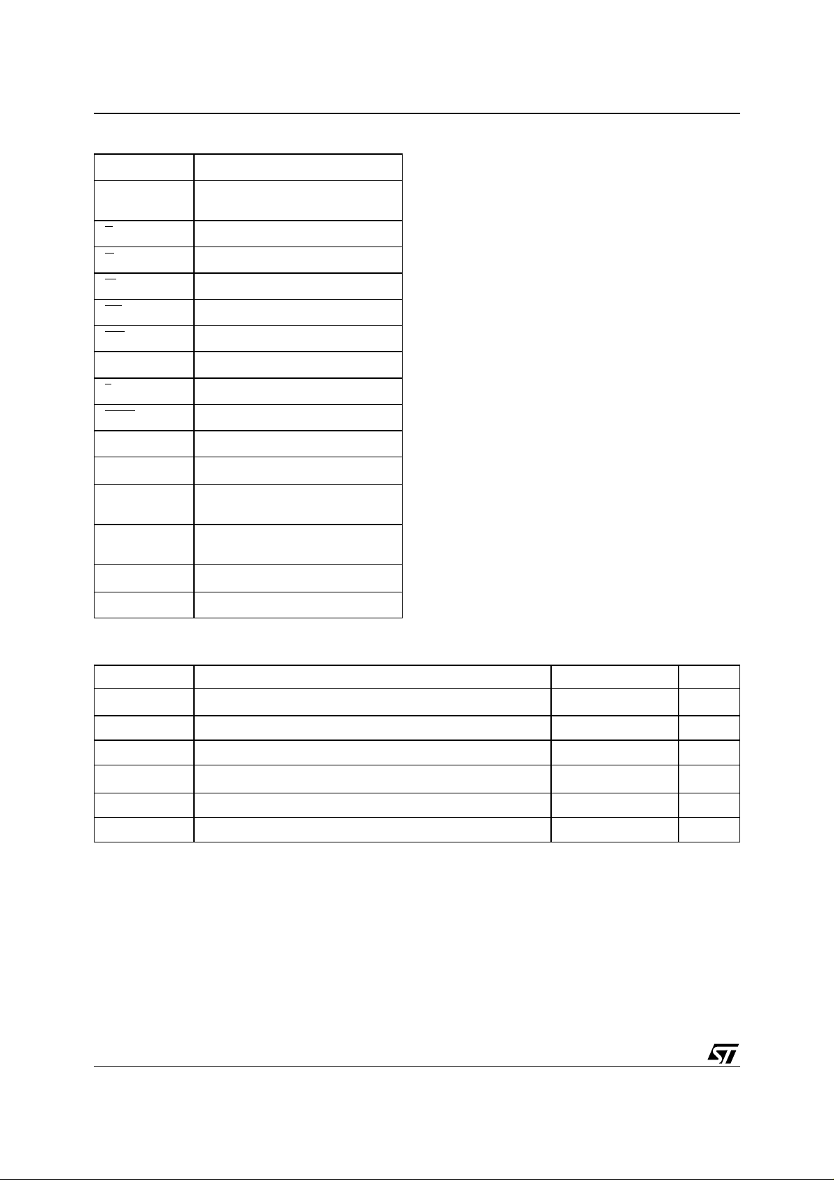
Figure 3. µBG A Co nn e ct i ons (Top view through pack a ge)
M59MR032C, M59MR032D
87654321
A
B
C
D
E
F
G
H
DU
DU
DU
DU
DDQ
SS
SS
SS
KWAIT
ADQ13 ADQ12
V
ADQ14ADQ15
DD
WV
WPRPBINVLA20A16V
ADQ2ADQ3ADQ6ADQ7V
ADQ10ADQ11ADQ4ADQ5V
V
109
A17
A19
PP
A18
ADQ8
ADQ9
V
ADQ1
DDQ
1211
DU
V
E
SS
G
ADQ0
DU
1413
DU
DU
AI90111
3/49
Page 4
M59MR032C, M59MR032D
Table 1. Signal Names
A16-A20 Address Inputs
ADQ0-ADQ15
E
G
W
RP
WP
K Burst Clock
L
WAIT
BINV Bus Invert
V
DD
V
DDQ
V
PP
V
SS
Data Input/Outputs or Address
Inputs, Command Inputs
Chip Enable
Output Enable
Write Enable
Reset/Power-down
Write Protect
Latch Enable
Wait Data in Burst Mode
Supply Voltage
Supply Voltage for Input/Output
Buffers
Optional Supply Voltage for
Fast Program & Erase
Ground
DESCRIPTION
The M59MR032 is a 32 Mbit non-volatile Flash
memory that m ay be erased electrically a t block
level and programmed in-system on a Word-byWord basis using a 1.65V to 2.0V V
supply for
DD
the circuitry. For Program and Erase operations
the necessary high voltages are g enerated internally. The device supports synchronous burst read
and asynchronous page mode read from all the
blocks of the memory array; at power-up the device is configured for page mode read. In synchronous burst mode, a new data is output at each
clock cycle for frequencies up to 54MHz.
The array matrix organization allows each block to
be erased and reprogrammed without affecting
other blocks. All blocks are protected against programming and erase at Power-up. Blocks can be
unprotected to make changes in the application
and then reprotected.
Instructions for Read/Reset, Auto Select, Write
Configuration Register, Programming, Block
Erase, Bank Erase, Erase Suspend, Erase Resume, Block Protect, Block Unprotect, Block Locking, CFI Query, are written to the memory through
a Command Interface (C.I.) using standard microprocessor write timings.
The memory is offered in LFBGA54 and µBGA46,
0.5 mm ball pitch packages and it is supplied wit h
all the bits erased (set to ’1’).
DU Don’t Use as Internally Connected
Table 2. Absolute Maximum Ratings
Symbol Parameter Value Unit
T
A
T
BIAS
T
STG
(3)
V
IO
, V
V
DD
DDQ
V
PP
Note: 1. Except for the ra ting "Oper at i ng Temperat ure Range", stresse s above those listed i n the Tabl e "Absolute M aximum Ratings" may
cause permanent damage to the device. These are stress ratings only and operation of the device at these or any other conditions
above those indi cated in t he Operating secti ons of thi s specif i cation is not imp l i ed. Exposure to Ab solute Maxi m um Rati ng condi tions for extended per iods may aff ect device reliabilit y. Refer also to the STMicroel ectronics SURE Program an d other relevan t qual ity docum en ts .
2. Depends on range.
3. Minimum Vol tage may undershoot to –2V during tr ansition and for less tha n 20ns.
Ambient Operating Temperature
Temperature Under Bias –40 to 125 °C
Storage Temperature –55 to 155 °C
Input or Output Voltage
Supply Voltage –0.5 to 2.7 V
Program Voltage –0.5 to 13 V
(1)
(2)
–40 to 85 °C
–0.5 to V
DDQ
+0.5
V
4/49
Page 5
M59MR032C, M59MR032D
Organization
The M59MR032 is org anized as 2Mbit by 16 bit s.
The first sixteen address lines are multiplexed with
the Data Input/Output signals on the m ultiplexed
address/data bus ADQ0-ADQ15. The remaining
address lines A16-A20 are the MSB addresses.
Memory control is provided by Chip Enable E
put Enable G
and Write Enable W inputs.
, Out-
The clock K input synchronizes the memory to the
microprocessor during burst read.
Reset RP
is used to reset all the memory circuitry
and to set the chip in power-down mode if this
function is enabled by a proper setting of the Configuration Register. Erase and Program operations
are controlled by an internal Program/Erase Controller (P/E.C.). Status Register data output on
ADQ7 provide s a Data Pollin g signal, ADQ6 and
ADQ2 provide Toggle signals and ADQ5 provides
error bit to indicate the state of the P/E.C operations. WAIT
output indicates to the microprocessor
the status of the memory during the burst mode
operations.
Table 3. Bank Size and Sectorization
Bank Size Parameter Blocks Main Blocks
Bank A 8 Mbit 8 blocks of 4 KWord 15 blocks of 32 KWord
Memory Blocks
The device features asymmetrically blocked architecture. M59MR032 has an array of 71 blocks and
is divided into two banks A and B, prov iding D ual
Bank operations. While programming or erasing in
Bank A, read operations are possible into Bank B
or vice versa. The memory also features an erase
suspend allowing to read or program in another
block within the same bank. Once suspended the
erase can be resumed. The Bank Size and Sectorization are summarized in Table 8. Parameter
Blocks are located at the top of the m emory address space for the M59MR032C, and at the bo ttom for the M59MR032D. The memory maps are
shown in Tables 4, 5, 6 and 7.
The Program and Erase operation s are managed
automatically by the P/E.C. Block protection
against Program or Erase provides additional data
security. Instructions are provided to protect or unprotect any block in the application. A second register locks the protection status while WP
is low
(see Block Lockin g description). All blocks are protected and unlocked at Power-up.
Bank B 24 Mbit - 48 blocks of 32 KWord
5/49
Page 6
M59MR032C, M59MR032D
Table 4. Bank A, Top Boot Block Addresses
M59MR032C
#
22 4 1FF000h-1FFFFFh
21 4 1FE000h-1FEFFFh
20 4 1FD000h-1FDFFFh
19 4 1FC000h-1FCFFFh
18 4 1FB000h-1FBFFFh
17 4 1FA000h-1FAFFFh
16 4 1F9000h-1F9FFFh
15 4 1F8000h-1F8FFFh
14 32 1F0000h-1F7FFFh
13 32 1E8000h-1EFFFFh
12 32 1E0000h-1E7FFFh
11 32 1D8000h-1DFFFFh
10 32 1D0000h-1D7FFFh
9 32 1C8000h-1CFFFFh
8 32 1C0000h-1C7FFFh
7 32 1B8000h-1BFFFFh
6 32 1B0000h-1B7FFFh
5 32 1A8000h-1AFFFFh
4 32 1A0000h-1A7FFFh
3 32 198000h-19FFFFh
2 32 190000h-197FFFh
1 32 188000h-18FFFFh
0 32 180000h-187FFFh
Size
(KWord)
Address Range
Table 5. Bank B, Top Boot Block Addresses
M59MR032C
#
47 32 178000h-17FFFFh
46 32 170000h-177FFFh
45 32 168000h-16FFFFh
44 32 160000h-167FFFh
43 32 158000h-15FFFFh
42 32 150000h-157FFFh
41 32 148000h-14FFFFh
40 32 140000h-147FFFh
39 32 138000h-13FFFFh
Size
(KWord)
Address Range
38 32 130000h-137FFFh
37 32 128000h-12FFFFh
36 32 120000h-127FFFh
35 32 118000h-11FFFFh
34 32 110000h-117FFFh
33 32 108000h-10FFFFh
32 32 100000h-107FFFh
31 32 0F8000h-0FFFFFh
30 32 0F0000h-0F7FFFh
29 32 0E8000h-0EFFFFh
28 32 0E0000h-0E7FFFh
27 32 0D8000h-0DFFFFh
26 32 0D0000h-0D7FFFh
25 32 0C8000h-0CFFFFh
24 32 0C0000h-0C7FFFh
23 32 0B8000h-0BFFFFh
22 32 0B0000h-0B7FFFh
21 32 0A8000h-0AFFFFh
20 32 0A0000h-0A7FFFh
19 32 098000h-09FFFFh
18 32 090000h-097FFFh
17 32 088000h-08FFFFh
16 32 080000h-087FFFh
15 32 078000h-07FFFFh
14 32 070000h-077FFFh
13 32 068000h-06FFFFh
12 32 060000h-067FFFh
11 32 058000h-05FFFFh
10 32 050000h-057FFFh
9 32 048000h-04FFFFh
8 32 040000h-047FFFh
7 32 038000h-03FFFFh
6 32 030000h-037FFFh
5 32 028000h-02FFFFh
4 32 020000h-027FFFh
3 32 018000h-01FFFFh
2 32 010000h-017FFFh
1 32 008000h-00FFFFh
0 32 000000h-007FFFh
6/49
Page 7
M59MR032C, M59MR032D
Table 6. Bank B, Bottom Boot Blo ck Addresses
M59MR032D
#
47 32 1F8000h-1FFFFFh
46 32 1F0000h-1F7FFFh
45 32 1E8000h-1EFFFFh
44 32 1E0000h-1E7FFFh
43 32 1D8000h-1DFFFFh
42 32 1D0000h-1D7FFFh
41 32 1C8000h-1CFFFFh
40 32 1C0000h-1C7FFFh
39 32 1B8000h-1BFFFFh
38 32 1B0000h-1B7FFFh
37 32 1A8000h-1AFFFFh
36 32 1A0000h-1A7FFFh
35 32 198000h-19FFFFh
34 32 190000h-197FFFh
33 32 188000h-18FFFFh
32 32 180000h-187FFFh
31 32 178000h-17FFFFh
30 32 170000h-177FFFh
29 32 168000h-16FFFFh
28 32 160000h-167FFFh
27 32 158000h-15FFFFh
26 32 150000h-157FFFh
25 32 148000h-14FFFFh
24 32 140000h-147FFFh
23 32 138000h-13FFFFh
22 32 130000h-137FFFh
21 32 128000h-12FFFFh
20 32 120000h-127FFFh
19 32 118000h-11FFFFh
18 32 110000h-117FFFh
17 32 108000h-10FFFFh
16 32 100000h-107FFFh
15 32 0F8000h-0FFFFFh
14 32 0F0000h-0F7FFFh
13 32 0E8000h-0EFFFFh
12 32 0E0000h-0E7FFFh
Size
(KWord)
Address Range
11 32 0D8000h-0DFFFFh
10 32 0D0000h-0D7FFFh
9 32 0C8000h-0CFFFFh
8 32 0C0000h-0C7FFFh
7 32 0B8000h-0BFFFFh
6 32 0B0000h-0B7FFFh
5 32 0A8000h-0AFFFFh
4 32 0A0000h-0A7FFFh
3 32 098000h-09FFFFh
2 32 090000h-097FFFh
1 32 088000h-08FFFFh
0 32 080000h-087FFFh
Table 7. Bank A, Bottom Boot Blo ck Addresses
M59MR032D
#
22 32 078000h-07FFFFh
21 32 070000h-077FFFh
20 32 068000h-06FFFFh
19 32 060000h-067FFFh
18 32 058000h-05FFFFh
17 32 050000h-057FFFh
16 32 048000h-04FFFFh
15 32 040000h-047FFFh
14 32 038000h-03FFFFh
13 32 030000h-037FFFh
12 32 028000h-02FFFFh
11 32 020000h-027FFFh
10 32 018000h-01FFFFh
9 32 010000h-017FFFh
8 32 008000h-00FFFFh
7 4 007000h-007FFFh
6 4 006000h-006FFFh
5 4 005000h-005FFFh
4 4 004000h-004FFFh
3 4 003000h-003FFFh
2 4 002000h-002FFFh
1 4 001000h-001FFFh
0 4 000000h-000FFFh
Size
(KWord)
Address Range
7/49
Page 8

M59MR032C, M59MR032D
SIGNAL DESCRIPTIONS
See Figure 1 and Table 1.
Address Inputs or Data Input/Output (ADQ0ADQ15). When Chip Enable E
put Enable G
is at VIH the multiplexe d address/
is at VIL and Out-
data bus is used to input addresses for the memory array, data to be programmed in the memory array or commands to be written to the C.I. The
address inputs for the memory array are latched
on the rising edge of Latch Enable L
latch is transparent when L
is at VIL. Both input
. The address
data and commands are latched on the rising edge
of Write Enable W
put Enable G
. When Chip Enable E and Out-
are at VIL the address/data bus outputs data from the Memory Array, the Electronic
Signature Manufacturer or Device codes, the
Block Protection status the Configuration Register
status or the Status Register Data Polling bit
ADQ7, the Toggle Bits ADQ6 and ADQ2, the Error
bit ADQ5. The address/data bus is high impedance when the chip is deselected, Output E nable
G
is at VIH, or RP is a t VIL.
Address Inputs (A16-A20). The five MSB addresses of the m emory array are latched on t he
rising edge of Latch Enable L
Chip Enable (E
). The Chip Enable input acti-
.
vates the memory control logic, input buffers, decoders and sense amplifiers. E
at VIH deselects
the memory and red uces the power consumption
to the standby level. E
can also be used to control
writing to the command register and to the memory array, while W
Output Enable (G
remains at VIL.
). The Output Enable gates the
outputs through the data buffers during a read operation. When G
is at VIH the outputs are High im-
pedance.
Write Enable (W
). This input controls writing to
the Command Register and Data latches. Data are
latched on the rising edge of W
.
Write Protect (WP
). This input gives an addition-
al hardware protection level against program or
erase when pulled at V
, as described in the Block
IL
Lock instruction description.
Reset/Power-down Input (RP
). The RP input
provides hardware reset of the memory, and/or
Power-down functions, depending on the Configuration Register status. Reset/Power-down of the
memory is achieved by pulling RP
least t
. When the reset pul se is given, if the
PLPH
to VIL for at
memory is in Read, Erase Suspend Read or
Standby, it will output new valid data in t
ter the rising edge of RP
. If the memory is in Erase
PHQ7V1
af-
or Program modes, the oper ation will be aborted
and the reset recovery will take a maximum of
. The memory will recover from Power-
t
PLQ7V
down (when enabled) in t
edge of RP
. Exit from Reset/Power-down changes
PHQ7V2
after the rising
the contents of the configuration register bits 14
and 15, setting the memory in asynchronous page
mode read and power save func tion disabled. All
blocks are protected and unlocked after a Reset/
Power-down. See Tables 29, 31 and Figure 14.
Latch Enable (L
). L latches the address bits
ADQ0-ADQ15 and A16-A20 on its rising edge.
The address latch is transparent when L
is at V
and it is inhibited when L is at VIH.
Clo c k (K). The clock input synchronizes the
memory to the microcontroller during burst mode
read operation; the address is latched on a K edge
(rising or falling, according to the configuration settings) when L
is at VIL. K is don’t care during asyn-
chronous page mode read and in write operations.
Wait (WAIT
). WAIT i s an output signal used dur-
ing burst mode read, indicating whet her the data
on the output bus are valid or a wait state must be
inserted. This output is high impedance when E
G
are high or RP is at VIL, and can be configured
or
to be active during the wait cycle or one clock cycle in advance.
IL
8/49
Page 9

M59MR032C, M59MR032D
Bus Invert (BINV). BINV is an input/output signal
used to reduce the amount of power needed to
switch the external address/data bus. The power
saving is achieved by inverting the dat a output on
ADQ0-ADQ15 every time this gives an advantage
in terms of number of toggling bits. In burst mode
read, each new data output from the memory is
compared with the previous data. If the number of
transitions required on the data bus is in excess of
8, the data is inverted and the BINV signal will be
driven by the memory at V
to inform the receiv-
OH
ing system that dat a must be inverted b efore any
further processing. By doing so, the act ual transitions on the data bus will be less than 8. In a similar way, when a command is given, BINV may be
driven by the s ystem a t V
to inform the memory
IH
that the data must be inverted.Like the other input/
output pins, BINV is high impedance when the
chip is deselected, output enable G
is at VIH or RP
is at VIL; when used as an input, BINV must follow
the same setup and hold timi ngs of the data inputs.
V
and V
DD
Supply Voltage (1.65V to 2.0V).
DDQ
The main power supply for all operations (Read,
Program and Erase). V
and V
DD
must be at
DDQ
the same voltage.
V
Program Supply Voltage (12V). VPP is
PP
both a control input and a power supply pin. T he
two functions are selected by the voltage range
applied to the pin; if V
range (0 to 2V) V
PP
is kept in a low vo ltage
PP
is seen as a control input, and
the current absorption is limited to 5µA (0.2µA typical). In this case with V
= VIL we obtain an ab-
PP
solute protection against program or erase; with
= V
V
PP
these functions are enabled. VPP val-
PP1
ue is only sampled during program or erase write
cycles; a change in its value after the operation
has been started does not have any effect and
program or erase are carried on regularly. If V
used in the 11.4V to 12. 6V range (V
) then the
PP2
PP
is
pin acts as a power suppl y. This supply voltage
must remain stable as long as program or eras e
are finished. In read mode the current sunk is less
then 0.5mA, while during program and erase operations the current may increase up to 10mA.
V
Ground. VSS is the reference for al l the vol t-
SS
age measurements.
9/49
Page 10
M59MR032C, M59MR032D
DEVICE OPERATIONS
The following operations can be performed using
the appropriate bus cycles: Address Latch, Read
Array (Random, and Page Modes), Write command, Output Disable, Standby, Reset/Powerdown and Block Locking. See Table 8.
Address Latch. In asynchronous operation, the
address is latched on the rising edge of L
burst mode, the address is latched either by L
input; in
going high or with a rising/fallin g edge of K , de pending on the clock configuration.
Read. Read operations are used to output the
contents of the Memory Array, the Electronic Signature, the Status Register, the CFI, the Block
Protection Status, the Configuration Register status and the Security Code.
Table 8. User Bus Operations
Operation E G W RP WP ADQ0-ADQ15
Write
Output Disable
Standby
Reset / Power-down X X X
Block Locking
Note: 1. X = Don’t care.
(1)
V
IL
V
IL
V
IH
V
IL
V
IH
V
IH
XX
XX
Read operation of the Memory Array may be performed in asynchronous page mode or synchronous burst mode. In asynchronous page mode
data is internally read and stored in a page buffer.
The page has a size of 4 words and is addres sed
by ADQ0 and ADQ1 address inputs.
According to the device configuration the following
Read operations: Electronic Signature - Status
Register - CFI - Block Protection Status - Configuration Register Status - Security Code must be accessed as asynchronous read or as single
synchronous burst mode (see Figure 4). Both Chip
Enable E
and Output Ena ble G must be at VIL in
order to read the output of the memory.
V
IL
V
IH
V
IH
V
IH
V
IH
V
IL
V
IH
V
IH
V
IH
V
IH
V
IH
V
IL
Data Input
Hi-Z
Hi-Z
Hi-Z
X
Table 9. Read Electronic Signature (AS and Read CFI instructions)
Code Device E
Manufacturer Code
M59MR032C
Device Code
M59MR032D
Note: 1. Addresses are l atched on the ri sing edge of L input.
V
IL
V
IL
V
IL
Table 10. Read Block Protection (AS and Read CFI instructions)
Block Status E
Protected and
unlocked
Unprotected and
unlocked
Protected and locked
Unprotected and
(2)
locked
Note: 1. Addresses are l atched on the ri sing edge of L input.
2. A locked blo ck can be unprot ected only wit h WP
V
IL
V
IL
V
IL
V
IL
G W A0-A7 A8-A11 A12-A20 Data
V
V
V
V
V
IL
IL
IL
IL
IH
V
IH
V
IH
V
IH
at V
G W A0-A7 A8-A20 Data
V
IL
V
IL
V
IL
V
IH
V
IH
V
IH
(1)
02h Don’t Care Block Address 0001
02h Don’t Care Block Address 0000
02h Don’t Care Block Address 0003
02h Don’t Care Block Address 0002
IH.
(1)
00h Don’t Care 0020h
01h Don’t Care 00A4h
01h Don’t Care 00A5h
10/49
Page 11
M59MR032C, M59MR032D
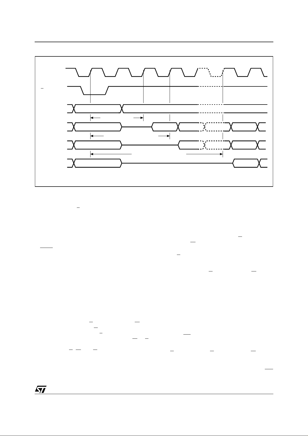
Figure 4. Read Operation Sequence wh en CR15 = 0 (excluding Read Me mory Array)
K
L
A16-A20
ADQ0-ADQ15
ADQ0-ADQ15
ADQ0-ADQ15
VALID ADDRESS
CONF. CODE 2
VALID ADDRESS VALID DATA NOT VALID
CONFIGURATION CODE 3
VALID ADDRESS VALID DATA
CONFIGURATION CODE 6
VALID ADDRESS VALID DATA
Burst Read. The device also supports a burst
read. In this mode, an address is first latched on
the rising edge of L
or K (or fallin g edge of K, according to configuration settings); after a configurable delay of 2 to 6 clock cycles a new data is
output at each clock cycle. The burst sequence
may be configured for linear o r interleaved order
and for a length of 4, 8 words or for continuous
burst mode.
A WAIT
signal may be asserted to indicate to the
system that an output delay will occur.
This delay will depend on the starting address of
the burst sequence; the worst case delay will occur when the sequence is crossing a 32 word
boundary and the starting address was at the end
of a four word boundary. See the Write Configuration Register (CR) Instruction for more details on
all the possible settings for the synchronous burst
read.
Write. Write operations are used to give I nstruction Commands to the memory or to latch Input
Data to be programmed. A write operation is initiated when Chip Enable E
with Output Enable G at VIH. Addresses are
at V
IL
latched on the rising edge of L
put Data are latched on the rising edge of W
and Write Enable W are
. Commands and In-
or E
whichever occurs first. Noise pulses of less than
5ns typical on E
, W and G signals do not start a
write cycle. Write operations are asynchronous
and clock is ignored during write.
Dual Bank Operations. The Dual Bank allows to
read data from one bank of memory while a pro-
NOT VALID
NOT VALID
AI90112
gram or erase operation is in progress in the other
bank of the memory. Read and Write cycles can
be initiated for simultaneous operations in different
banks without any d elay. Status Register du ring
Program or Erase must be monitored using an address within the bank being modified.
Output Disa bl e . The data outputs are high impedance when the Output Enable G
Write Enable W
at VIH.
is at VIH with
Standby. The mem ory is in standby when C hip
Enable E
is at VIH and the P/E.C. is idle. The power consumption is reduced to the standby level
and the outputs are high impedance, independent
of the Output Enable G
or Write Enable W input s.
Automatic Standby. When in Read mode, after
150ns of bus inactivity and when CMOS levels are
driving the addresses, the chip automatically enters a pseudo-standby mode where consumption
is reduced to the CMOS standby value, while outputs still drive the bus. The automatic standby feature is not available when the device is configured
for synchronous burst mode.
Power-down. The memory is in Power-down
when the Configuration Register is set for Powerdown and RP
is at VIL. The power consumption is
reduced to the Power-down level, and Outputs are
in high impedance, independent of the Chip Enable E
, Output Enable G or Write Enable W inputs.
Block Locking. Any combination of blocks can
be temporarily protected against Program or
Erase by setting the lock register and pulling WP
to VIL (see Block Lock instruction).
11/49
Page 12
M59MR032C, M59MR032D
INSTRUCTIONS AND COMMANDS
Seventeen instructions are defined (see Table
17), and the internal P/E.C. automatically handles
all timing and verification of the Program and
Erase operations. The Status Register Dat a Polling, Toggle, Error bits can be read at any time, during programming or erase, to monitor the progress
of the operation.
Instructions, made up of one or more com mands
written in cycles, can be given to the Program/
Erase Controller through a Command Interface
(C.I.). The C.I. latches comma nds written to the
memory. Commands are made of address and
data sequences. Two Coded Cycles unlock the
Command Interface. They are followed by an input
command or a confirmation command. The Coded
Sequence consists of writing the dat a AAh at the
address 555h during the f irst cycle and the data
55h at the address 2AAh during the second cycle.
Instructi ons a re co mpose d of up to si x cycles. The
first two cycles input a Coded Sequence to the
Command Interface which is common to all instructions (see Table 17). T he third cycle inputs
the instruction set-up command. Subseq uent cycles output the addressed data, Elect ronic Signature, Block Protection, Configuration Register
Status or CFI Query for Read operations. In order
to give additional data protection, the instructions
for Block Erase and Bank Erase require further
command inputs. For a Program instruction, the
fourth command cycle inputs the address and data
to be programmed. For a Double Word Programming instruction, the fourth and fifth co mmand cycles input the address and data to be
programmed. For a Block Eras e and Bank Erase
instructions, the fourth and fifth cycles input a further Coded Sequence before the Erase confirm
command on the sixth cycle. Any combination of
blocks of the same memory bank can be erased.
Erasure of a memory block may be suspended, in
order to read data from another block or to program data in another block, and then resumed.
When power is first applied the command interface
is reset to Read Array.
Command sequencing must be followed exactly.
Any invalid combination of commands will reset
the device to Read Array. The inc reased number
of cycles has been chosen to ensure maximum
data security.
Read/Reset (RD) Instruction. The Read/Reset
instruction consists of one write cycle giving the
command F0h. It can be optionally preceded by
the two Coded Cycles. Subsequent read operations will r ead the memory array a ddressed and
output the data read. The Reset com mand does
not affect the configurati on of unprotected blo cks
and the Configuration Register status. Read/Reset Instruction is ignored when program or erase is
in progress.
CFI Query (RCFI) Instruction. Common Flash
Interface Query mode is entered writing 98h at address 55h. The CFI data structure gives information on the device, such as the sectorization, the
command set and some el ectrical specifications.
Tables 19, 20, 21 and 22 show the addresses
used to retrieve each data. The CFI data structure
contains also a se curity area; in this section, a 64
bit unique security number, organ ized by word, is
written starting at address 81h. This area can be
accessed only in read mode by the final user and
there are no ways of changing the code after it has
been written by ST. Write a read instruction (RD)
to return to Read Array mode.
Table 11. Commands
Hex Code Command
00h Bypass Reset
10h Bank Erase Confirm
20h Unlock Bypass
30h Block Erase Resume/Confirm
40h Double Word Program
Block Protect, or
60h
80h Set-up Erase
90h
98h CFI Query
A0h Program
B0h Erase Suspend
F0h Read Array/Reset
Block Unprotect, or
Block Lock, or
Write Configuration Register
Read Electronic Signature, or
Block Protection Status, or
Configuration Register Status
12/49
Page 13
M59MR032C, M59MR032D
Auto Select (AS) Instruction. This instruc-
tion uses two Coded Cycles followed by one write
cycle giving the command 90h to address 555h for
command set-up. A subsequent read will output
the Manufacturer or the Device Code (Electronic
Signature), the Block Protection status or the Configuration Register status depending on the levels
of ADQ0 and ADQ1 (see Tables 9, 10 and 11).
The Electronic Signature can be read from the
memory allowing programming equipment or applications to automatic ally match their interface to
the characteristics of M59MR032. The Manu facturer Code is output when the address lines ADQ0
and ADQ1 are at V
when ADQ0 is at V
, the Device Code is output
IL
with ADQ1 at VIL.
IH
The codes are output on ADQ0-ADQ7 with ADQ8ADQ15 at 00h. The A S ins truction also allows the
access to the Block Protection Status. After giving
the AS instruction, ADQ0 is set to V
, while A12-A20 define the address of the
at V
IH
with ADQ1
IL
block to be verified (see Table 10). The AS Instruction finally allows the access to the Configuration
Register status if both ADQ0 and ADQ1 are set to
V
; refer to Table 12 for configuration register de-
IH
scription.
A reset command puts the device in Read Array
mode.
Write Configuration Register (CR) Instruction. This instruction uses t wo Coded Cyc les fol-
lowed by one write cycle giving the command 60h
to address 555h. A further write cycle giving the
command 03h writes the cont ents of address bi ts
ADQ0-ADQ15 to bits CR15-CR0 of the configuration register. At Power-up the Configu ration Register is set to asynchronous Read mode, Powerdown disabled and bus invert (power save function) disabled.
A description of the effects of each configuration
bit is given in Table 12.
Table 12. Read Configuration Register (AS and Read CFI instructions)
Configuration Register Function
Read mode
CR15
CR14
CR13-CR11
CR10
CR9
CR8
CR7
CR6
CR5-CR3 Reserved
CR2-CR0
0 = Burst mode read
1 = Page mode read (default)
Bus Invert configuration (power save)
0 = disabled (default)
1 = enabled
X-Latency
010 = 2 clock latency
011 = 3 clock latency
100 = 4 clock latency
101 = 5 clock latency
110 = 6 clock latency
Power-down configuration
0 = power-down disabled (default)
1 = power-down enabled
Data hold configuration
0 = data output at every clock cycle
1 = data output every 2 clock cycles
Wait configuration
0 = WAIT
1 = WAIT
Burst order configuration
0 = Interleaved
1 = Linear
Clock configuration
0 = Address latched and data output on the falling clock edge.
1 = Address latched and data output on the rising clock edge.
Burst length
001 = 4 word burst length
010 = 8 word burst length
111 = Continuous burst mode (requires CR7 = 1)
is active during wait state
is active one data cycle before wait state
13/49
Page 14
M59MR032C, M59MR032D
Table 13. X-Latency Configuration
Configuration Code
2 25MHz 20MHz
3 40MHz 30MHz
4 54MHz 40MHz
(1)
5
(1)
6
Note: 1. Configurati on codes 5 and 6 may be used only in conjunct i on with configuration bit CR9 set at “1” (one data ever y 2 clock cycles).
100ns 120ns
66MHz 50MHz
– 60MHz
Figure 5. X-L at ency Configu ra ti on Sequenc e
K
L
Input Frequency
A16-A20
ADQ0-ADQ15
ADQ0-ADQ15
ADQ0-ADQ15
VALID ADDRESS
CONF. CODE 2
VALID ADDRESS VALID DATA VALID DATA
CONFIGURATION CODE 3
VALID ADDRESS VALID DATA
CONFIGURATION CODE 6
VALID ADDRESS VALID DATA
– Read mode (CR15). The device supports an
asynchronous page mode and a synchronous
burst mode. In asynchrono us page mode, the
default at power-up, data is internally read and
stored in a buffer of 4 words selected by ADQ0
and ADQ1 address inputs. In synchronous burst
mode, the device latches the starting address
and then outputs a sequence of data which depends on the configuration register settings.
– Bus Invert configuration (CR14). This regis-
ter bit is used to enable the BINV pin functionality. BINV functionality depends upon
configuration bits CR14 and CR15 (see Table
12 for configuration bits definition) as shown in
Table 14.
VALID DATA
VALID DATA
AI90113
As output p in BINV is active only wh en enabled
(CR14 = 1) in Read Array burst mode (CR15 = 0).
As input pin BINV is active only when enabled
(CR14 = 1). BINV is ignored when ADQ0ADQ15 lines are used as address inputs (addresses must not be inverted).
Table 14. BINV Configuration Bits
CR15 CR14
00X0
0 1 Active Active
10X0
1 1 Active 0
BINV
IN OUT
14/49
Page 15
M59MR032C, M59MR032D
Table 15. Burst Order and Length Configuration
Starting
Address
0 0-1-2-3 0-1-2-3 0-1-2 -3-4-5 -6-7 0-1-2-3-4-5-6-7 0-1-2 -3-4-5 ...
1 1-2-3-0 1-0-3-2 1-2-3 -4-5-6 -7-0 1-0-3-2-5-4-7-6 1-2-3 -4-5-6 ...
2 2-3-0-1 2-3-0-1 2-3-4 -5-6-7 -0-1 2-3-0-1-6-7-4-5 2-3-4 -5-6-7 ...
3 3-0-1-2 3-2-1-0 3-4-5 -6-7-0 -1-2 3-2-1-0-7-6-5-4 3-4-5 -6-7-8 ...
...
7 7-4-5-6 7-6-5-4 7-0-1 -2-3-4 -5-6 7-6-5-4-3-2-1-0 7-8-9-10-11...
...
28 28-29-30-31- 32...
29 29-30-31-WAIT-32...
30 30-31-WAIT-WAIT-32...
31 31-WAIT-WAIT-WAIT-32...
Linear Interle aved L inear Interleaved
4 Words 8 Words
Continuous Burst
– X-Latency (CR13-CR11). These configuration
bits define the number of clock cycles ela psing
going low to valid data available in b urst
from L
mode. The correspondence between X-Latency
settings and the sustainable clock freq uencies
is given in Table 13 and Figure 5.
– Power-down configuration (CR10). The RP
pin may be configured to give a very low power
consumption when driven low (power-down
state). In power-down the I
supp ly cu rre nt is
CC
reduced to a typical figure of 2µA; if this function
is disabled (default at power-up) the RP
pin
causes only a reset of the device and the supply
current is the stand-by value. The recovery time
after a RP
pulse is significantly longer (50µs vs.
150ns) when power-down is enabled.
– Data hold configuration (CR9). In burst
mode this register bit determines if a new data
is output at each clock cycle or every 2 clock cycles.
– Wait configuration (CR8). In burst mode
indicates whether the data on the ou tput
WAIT
bus are valid or a wait s tate must be inserted.
The configuration bit determines if WAIT
will be
asserted one clock cycle before the wait state or
during the wait state (see Figure 10).
– Burst order configuration (CR7). See Table
15 for burst order and length.
– Clock c o nf ig uration (CR 6) . In burst mode de-
termines if address is latched and data is output
on the risin g o r falling edge of th e clo ck.
– Burst length (CR2-CR0). In burst mode deter-
mines the number of words output by the memory. It is possible to have 4 words, 8 words or a
continuous burst mode, in which all the words in
bank A or bank B are read sequentia lly. In continuous burst mode the burst sequenc e is in terrupted at the end of each o f the two banks or
when a suspended block is reached. In continuous burst mode it may happen that the memory
will stop the data output flow for a few clock cycles; this event is signaled by WAIT
going low
until the output flow is resumed. The initial address determines if the output delay will occur
as well as its duration. I f t he st arting a ddres s is
aligned to a four word boundary no wait sta tes
will be needed. If the starting address is shi fted
by 1,2 or 3 pos itions f rom t he four word b oundary, WAIT
will be asserted for 1,2 or 3 clock cy-
cles (2,4, 6 cycles if CR9 is set at “1”) when the
burst sequence is crossing the first 32 word
boundary. WAIT
will be asserted only once dur-
ing a continuous burst access. See also Table
15.
Enter Bypass Mode (EBY) Instruction. This instruction uses the two Coded cycles f ollowed by
one write cycle giving the command 20h to address 555h for mode set-up. Once in Bypass
mode, the device will accept the Exit Bypass
(XBY) and Program or Double Word Program in
Bypass mode (PGBY, DPGBY) commands. The
Bypass mode allows to reduce the overall programming time when large memory arrays need to
be programmed.
Exit B y pa ss Mode (XBY) Ins t r uc tion . This instruction uses two write cycles. The first inputs to
the memory the command 90h and the second inputs the Exit Bypass mode confirm (00h). After the
XBY instruction, the device resets to Read Memory Array mode.
15/49
Page 16

M59MR032C, M59MR032D
Table 16. Protection States
Current State
(WP
, ADQ1,
ADQ0)
100 yes 101 100 111 000
101 no 101 100 111 001
110 yes 111 110 111 011
111 no 111 110 111 011
000 yes 001 000 011 100
001 no 001 000 011 101
011 no 011 011 011
Note: 1. All blo cks are protected at power-up, so the default configuration i s 001 or 101 according to WP status.
2. Current st at e and Next state gives the protection status of a block . The protection status is defined by the write protect pin and by
ADQ1 (= 1 for a locked block) and ADQ0 (= 1 for a protected block) as read in the Autoselect instruction with A1 = V
3. Next state is the protection status of a block after a Protect or Unprotect or Lock command has been issued or after WP
its logic value.
4. A WP
(2)
Program/Erase
Allowed
transition to VIH on a locked block will restore the previous ADQ0 value, giving a 111 or 110.
Program in Bypass Mode (PGBY) Instruction. This instruction uses two write cycles. T he
Program command A0h is written to any Address
on the first cycle and the second write cycle latches the Address on the rising edge of L
Data to be written on the rising edge of W
starts the P/E.C. Read operations within the same
bank output the St at us Register bi ts aft er the programming has started. Memory programming is
made only by writing ’0’ in place of ’1’ . The content
of the memory cell is not changed if the user write
’1’ in place of ’0’ and no error occurs. Status bits
ADQ6 and ADQ7 determine if programming is ongoing and ADQ5 allows verification of any possible
error.
Program (PG) Instruction. This ins truction uses
four write cycles. The Program command A0h is
written to address 555h on the third cycle after two
Coded Cycles. A fourth write operation latches the
Address and the Dat a to be writte n a nd starts the
P/E.C. Read operations within the same bank output the Status Register bits after the programming
has started. Memory program ming is made only
by writing ’0’ in place of ’1’. The content of the
memory cell is not changed if the user write ’1’ in
place of ’0’ and no error occurs. Status bits ADQ6
and ADQ7 determine if program ming is on-going
and ADQ5 allows verification of any possible error.
Programming at an address not in blocks being
erased is also possible during erase suspend.
Double Word Program (DPG) Instruction. This
feature is offered to improve the programming
throughput, writing a page of two adjacent words
(1)
Next State After Event
Protect Unprotect Lock WP transition
(3)
111 or 110
in parallel. High voltage (11.4V to 12.6V) on V
pin is required. This instruction uses five write cycles. The double word program command 40h is
written to address 555h on the third cycle after two
and the
and
Coded Cycles. A fourth write cycle latches the address and data to be written to the first location. A
fifth write cycle latches the new data to be written
to the second location and starts the P/E.C.. Note
that the two locations must have the same address
except for the address bit A0. The Double Word
Program can be executed in Bypass mode (DPGBY) to skip the two coded cycles at the beginning
of each command.
Block Protect (BP), Blo ck Unprotect (BU),
Block Lock (BL) Instructions. All bl ocks are
protected and unlocked at power-up. Each block
of the array has two levels of protection against
program or erase operation. The first level is set by
the Block Protect instruction; a protected block
cannot be programmed or erased until a Block Unprotect instruction is given for that block. A second
level of protection is set by the Block Lock instruction, and requires the use of the WP
pin, according
to the following scheme:
– when WP
is at VIH, the Lock status is overridden
and all blocks can be protected or unprotected;
– when WP
is at VIL, Lock status is enabled; the
locked blocks are protected, regardless of their
previous protect state, and protection status
cannot be changed. Bloc ks that are not locked
can still change their protection status, and program or erase accordingly;
(4)
and A0 = VIL.
IH
has changed
PP
16/49
Page 17

M59MR032C, M59MR032D
– the lock status is clea red for a ll blocks a t p ower-
up or pulling R P
at VIL for at least t
PLPH
. The
protection and lock statu s can be monitored for
each block using the Autoselect (AS) instruction. Pr o tected bloc k s w ill o ut p ut a ‘1’ on ADQ0
and locked blocks will output a ‘1’ on ADQ1.
After a pulse of RP
of at least t
all blo c ks a r e
PLPH
protected and unlocked.
Refer to Table 16 for a list of the protection states.
Block Erase (BE) Instruction. This instruction
uses a minimum of six write cycles. The Erase
Set-up command 80h is written to ad dress 555h
on third cycle after the two Coded cycles. The
Block Erase Confirm command 30h is similarly
written on the sixt h cycle after another two Coded
cycles and an address within the block to be
erased is given and latched into the memory.
Additional block Erase Confirm commands and
block addresses can be written subsequently to
erase other blocks i n paral l el, wit h out fu rthe r Co ded cycles. All blocks must belong to the same
bank of memory; if a new block belonging to the
other bank is given, the operation is aborted. The
erase will start after an erase timeout period of
100µs. Thus, additional Erase Confirm commands
for other blocks must be given within this delay.
The input of a new Erase Confirm command will
restart the timeout period. The status of the in ternal timer can be monitored through the level of
ADQ3, if ADQ3 is '0' the Block Erase Comm and
has been given and the timeout is running, if
ADQ3 is '1', the tim eout has expired and the P/
E.C. is erasing the Block(s). If the second command given is not an erase confirm or if the Coded
cycles are wrong, the instruction aborts, and the
device is reset to Read Array. It is not necessary
to program the block with 00h as the P/E.C. will do
this automatically before erasing to FFh. Read operations within the same bank, after the sixth rising
edge of W
or E, output the status register bits.
During the execution of the erase by the P/E.C.,
the memory accepts only the Erase Suspend ES
instruction; the Read/Reset RD instruction is accepted during the 100µs time-out period. Data
Polling b it ADQ7 ret u r ns '0 ' w h ile the erasure is in
progress and '1' when it has com pleted. The Toggle bit ADQ6 tog gles during the erase operation,
and stops when erase is completed.
After completion the Status Register bit ADQ5 returns '1' if there has been an erase failure. In such
a situation, the Toggle bit ADQ2 c an be used to
determine which block is not correctly erased. In
the case of erase failure, a Read/Reset RD instruction is necessary in order to reset the P/E.C.
Bank Erase (BKE) Instruction. This instruction
uses six write cycl es and is use d to erase all t he
blocks belonging to the selected bank . T he E rase
Set-up command 80h is written to address 555h
on the third cycle after the two Coded cycles. The
Bank Erase Confirm command 10h is similarly
written on the sixt h cycle after another two Coded
cycles at an address within the selected bank. If
the second command gi ven is not an erase confirm or if the Coded cycles are wrong, the instruction aborts and the device is reset to Read Array.
It is not necessary to program the array with 00h
first as the P/E.C. will automatically do this before
erasing it to FFh. Read operations within the same
bank after the sixth rising edge of W
or E output
the Status Register bits. During the execution of
the erase by the P/E.C., Data Polling bit ADQ7 returns '0', then '1' on completion. The Toggle bit
ADQ6 toggles during erase operation and stops
when erase is completed. After completion the
Status Register bit ADQ5 returns '1' if there has
been an Erase Failure.
Erase Suspend (ES) Instruction. In a dual bank
memory the Erase Suspend instruction is used to
read data within the bank where erase is in
progress. It is also possible to program data in
blocks not being erased.
The Erase Suspend in struction con sists o f writing
the command B0h without any s pecific address.
No Coded Cycles are requ ired. Erase s uspend is
accepted only during the Block Erase i nstruction
execution. The Toggle bit ADQ6 stops toggling
when the P/E.C. is suspended within 15µs after
the Erase Suspend (ES) command has been written. The device will then automatically be set to
Read Memory Array mode. When erase is suspended, a Read from blocks being erased will output ADQ2 toggling and ADQ 6 at '1'. A Read from
a block not being erased returns valid data. During
suspens ion the memory w ill respond only to the
Erase Resume ER and the Program PG instructions. A Program operation can be initiated during
erase suspend in one of the blocks not being
erased. It will result in ADQ6 toggling when the
data is being programmed.
Erase Resume (ER) Instruction. If an Erase
Suspend instruction was previously exec uted, the
erase operation may be resumed by giving the
command 30h, at an address within the bank being erased and without any Coded Cycle.
17/49
Page 18

M59MR032C, M59MR032D
Table 17. Instructions
(1,2)
Mne. Instr. Cyc. 1st Cyc. 2nd Cyc. 3rd Cyc. 4th Cyc. 5th Cyc. 6th Cyc.
RD
Read/Reset
(4)
Memory Array
(3)
Addr.
1+
Data F0h
Addr. 555h 2AAh 555h
3+
Data AAh 55h F0h
X
Read Memory Array until a new write cycle is initiated.
Read Memory Array until a new
write cycle is initiated.
Addr. 55h
RCFI CFI Query 1+
Read CFI data until a new write cycle is initiated.
Data 98h
Addr. 555h 2AAh 555h Read electronic Signature or
AS
(4)
Auto Select 3+
Configuration
CR
Register Write
Data AAh 55h 90h
Addr. 5 55h 2AAh 555h
4
Block Protection or Configuration
Register Status until a new cycle
is initiated.
Configuration Data
Data AAh 55h 60h 03h
Program
Address
Program
Data
Program
Address 1
Program
Data 1
Read Data Polling or
Toggle Bit until
Program completes.
Program
Address 2
Note 6, 7
Program
Data 2
PG Program 4
EBY
XBY
Double Word
Program
Enter Bypass
Mode
Exit Bypass
Mode
DPG
Addr. 555h 2AAh 555h
Data AAh 55h A0h
Addr. 5 55h 2AAh 555h
5
Data AAh 55h 40h
Addr. 555h 2AAh 555h
3
Data AAh 55h 20h
Addr. XX
2
Data 90h 00h
PGBY
Program in
Bypass Mode
Double Word
DPGBY
Program in
Bypass Mode
BP Block Protect 4
BU Block Unprotect 1
18/49
Addr. X
2
Data A0h
Addr. X
Program
Address
Program
Data
Program
Address 1
Read Data Polling or Toggle Bit until Program
completes.
Program
Address 2
3
Data 40h
Program
Data 1
Program
Data 2
Addr. 555h 2AAh 555h
Data AAh 55h 60h 01h
Addr. 555h 2AAh 555h
Data AAh 55h 60h D0h
Note 6, 7
Block
Address
Block
Address
Page 19

M59MR032C, M59MR032D
Mne. Instr. Cyc. 1st Cyc. 2nd Cyc. 3rd Cyc. 4th Cyc. 5th Cyc. 6th Cyc.
BL Block Lock 4
Addr. 555h 2AAh 555h
Data AAh 55h 60h 2Fh
Block
Address
BE Block Erase 6+
Addr. 555h 2AAh 555h 555h 2AAh
Data AAh 55h 80h AAh 55h 30h
Addr. 555h 2AAh 555h 555h 2AAh
BKE Bank Erase 6
Data AAh 55h 80h AAh 55h 10h
ES Erase Suspend 1
ER Erase Resume 1
(3)
Addr.
Data B0h
Addr.
X
Bank
Address
Read until Toggle stops, then read all the data needed
from any Blocks not being erased then Resume Erase.
Read Data Polling or Toggle Bits until Erase completes or
Erase is suspended another time
Data 30h
Note: 1. Commands not interpreted in this table will default to read array mode.
2. For Coded cycles address inputs A11-A20 are don’t care.
3. X = Don’t Care.
4. The first cy cl es of the RD or AS in struction s are follo wed by read operations. Any number of read cycles can occur after the command cycl e s.
5. During Era se Suspend, R ead and Data P rogram funct i ons are allowed in blocks not being erased.
6. Program Address 1 and Program Address 2 must be consecuti ve addresses di f fering only fo r address bit A0.
7. High voltage on V
(11.4V to 12.6V) is required for th e proper execution of the Double Wo rd Program in st ruction.
PP
Block
Address
Bank
Address
19/49
Page 20

M59MR032C, M59MR032D
STATUS REGISTER BITS
P/E.C. status is indicated during execution by Data
Polling on ADQ 7, detection of Toggle on ADQ6
and ADQ2, or Error on ADQ5 b its. Any read attempt within the Bank being modified and du ring
Program or Erase comm and execution will automatically output these five Status Register bits.
The P/E.C. a utomatically sets bits ADQ2, ADQ5,
ADQ6 and ADQ7. Ot her b its (ADQ0, ADQ1 and
ADQ4) are reserved for future use and should be
masked (see Ta ble 18). Read attempts within t he
bank not being modified will output array data.
Toggle bits ADQ6 and ADQ2 are affected by G
and/or E cycles regardless of the bank in which
these cyc les refe r to . Thi s me an s tha t tog gle bits
are in a state that d epends on the amount of ac cesses to both banks and not only to the bank
where erasing or programming is on going. Status
Register Bits m ust be accesse d according to the
device configuration (see Figure 4).
Data Polling Bit (ADQ7). When Programming
operations are in progress, this bit outputs the
complement of the bit being programmed on
ADQ7. In case of a double word program operation, the complement i s done on ADQ7 of the la st
word written to the command interface, i.e. the
data written in the fifth cycle. During Erase operation, it outputs a ’0’. After completion of the operation, ADQ7 will output the bit last programmed or
a ’1’ af ter erasing. Data Polling is valid and only effective during P/E.C. operation, that is after the
fourt h W
W
pulse for programming or after the sixth
pulse for erase. It must be performed at the address being programmed or at an address within
the block being erased. See Figure 17 for the Data
Polling flowchart and Figure 15 for the Data Polling
waveforms. ADQ7 will also flag the Erase Suspend mode by swi tching from ’0’ to ’1’ at the s tart
of the Erase Suspend. In order to monitor ADQ7 in
the Erase Suspend mode an address within a
block being erased must be provided. For a Read
Operation in Suspend mode, AD Q7 will output ’1’
if the read is attempted on a block being erased
and the data value on other blocks. During Program operation in Erase Suspend Mode, ADQ7
will have the same behavior as in the normal program execution outside of the suspend mode.
Toggle Bit (A D Q6). When Programming or Erasing operations are in progress, successive attempts to read ADQ6 will output complemen tary
data. ADQ6 will toggle following toggli ng of either
G
, or E when G is a t VIL. The operation is completed when two successive reads yield the same output data. The next read will output the bit last
programmed or a ’1’ after erasing. The toggle bit
ADQ6 is valid only during P /E.C. operations, that
is after the fourth W
the sixth W
pulse for Erase. ADQ6 will be set to ’1’
pulse for programming or after
if a Read operation is attempted on an Erase Suspend block. When erase is suspended A DQ6 will
toggle during programming operations in a block
different from the block in Erase Suspend. Either
or G toggling will cause ADQ6 to toggle. See
E
Figure 18 for Toggle Bit flowchart and Figure 16
for Toggle Bi t waveforms.
Toggle Bit (A D Q2). This toggle bit, togeth er with
ADQ6, can be used to determine the device status
during the Erase operations. During Erase Suspend a read from a block being erased will cause
ADQ2 to toggle. A read from a block not being
erased will output data. ADQ2 will be set to ’1’ during program operation. After erase completion and
if the error bit ADQ 5 is set to ’1’, ADQ2 w ill togg le
if the faulty block is addressed.
Error Bit (ADQ5). This bit is set to ’1’ by the P/
E.C. when there is a failure of programming or
block erase, that results in invalid data in the memory block. In case of an error in block erase or program, the block in which the error occurred or to
which the programmed data belongs, must be discarded. Other Blocks may still be used. The error
bit resets after a Read/Reset (RD) instruction. In
case of success of Program or Erase, the error bit
will be set to ’0’.
Erase Timer Bit (ADQ3). This bit is set to ‘0’ b y
the P/E.C. when the last block Erase command
has been entered to the Command Interface and it
is awaiting the Erase start. When the erase timeout period is finished, ADQ3 returns to ‘1’, in the
range of 80µs to 120µs.
20/49
Page 21

M59MR032C, M59MR032D
Table 18. Status Register Bits
Program DQ7
Block Erase Timeout 0 Toggle 0 0 N/A
In Progress
Successfully/
Completed
Exceeded
Time Limit
Note: 1. Status Register bits do not consider BINV.
2. DQ7 and DQ2 r equire a valid address wh en reading status inform ation.
Block/Chip Erase 0 Toggle 0 1 N/A
Erase Suspend
Mode
Programming during Erase Suspend DQ7
Word Program
Block/Chip Erase
Word Program DQ7
Block/Chip Erase 0 Toggle 1 1
Program in Suspend DQ7
(1)
Status
Erase Suspended Block 1 1 0 N/A Toggle
Non Erase Suspended Block Automatic return to reading array data
(2)
DQ7
DQ6 DQ5 DQ3
Toggle 0 N/A 1
Toggle 0 N/A 1
Automatic return to reading array data
Toggle 1 N/A 1
Toggle 1 N/A 1
(2)
DQ2
Toggle is
failed, block is
addressed
POWER CONSUMPTION
Power-down
The memory pro vides Reset/P ower-down control
input RP
. The Power-down function can be activated only if the relevant Configuration Register bit
is set to ’1’. In this case, when the RP
pulled at V
I
(see Table 28), the memory is deselected and
CC2
the supply current drops to typically
SS
the outputs are in high impedance.If RP
to V
during a Program o r Erase operation, this
SS
operation is aborted in t
and the memory
PLQ7V
signal is
is pulled
content is no longer valid (see Reset/Power-down
input description).
Power-up
The memory Command Interface is reset on Power-up to Read Array. Either E
V
during Power-up to allow maximum security
IH
or W must be tied to
and the possibility to write a command on the first
rising edge of W
. At Power-up the device is config-
ured as:
– page mode: (CR15 = 1)
– power-down disabled: (CR10 = 0)
– BINV disabled: (CR14 = 0)
and all blocks are protected and unlocked.
Supply Rails
Normal precautions must be taken for supply voltage decoupling; each device in a system should
have the V
itor close to the V
rails decoupled with a 0.1µF capac-
DD
DD
, V
and VSS pins. The PCB
DDQ
trace widths should be sufficient to carry the required V
program and erase currents.
DD
21/49
Page 22

M59MR032C, M59MR032D
COMMON FLASH INTERFACE (CFI)
The Comm on Fl ash In ter fac e (C FI) spec if i cati on i s
a JEDEC approved, standardised data structure
that can be read from the Flash memory device.
CFI allows a syste m software to query the flash
device to determine various electrical a nd timing
parameters, density information and functions
supported by the device. CFI allows the system to
easily interface to the Flash memory, to learn
about its features and parameters, enabling the
software to configure itself when necessary.
Tables 19, 20, 21, 22, 23 and 24 show the address
used to retrieve each data.
The CFI data structure gives information on the
device, such as the sectorization, the command
set and some electrical specifications. Tab les 19,
20, 21 and 22 show the addresses used to retrieve
each data. The CFI data structure contains also a
security area; in this section, a 64 bit unique security number is written, starting at address 81h. This
area can be accessed only in read mode and there
are no ways of changing the code after it has been
written by ST. Write a read instruction to return to
Read mode. Refer to the CFI Query instruction to
understand how the M59MR032 enters the CFI
Query mode.
Table 19. Query Structure Overvi ew
Offset Sub-section Name Description
00h Reserved Reserved for algorithm-specific information
10h CFI Query Identification String Command set ID and algorithm data offset
1Bh System Interface Information Device timing & voltage information
27h Device Geometry Definition Flash device layout
P Primary Algorithm-specific Extended Query table
A Alternate Algorithm-specific Extended Query table
Note: The Flash memory di splay the CFI data structure whe n CFI Query comm and is is sued. In thi s table are lis ted the m ai n sub-se ctions
detailed in Ta bl es 20, 21 and 22 . Query data are al ways presented on the lowest order data outputs.
Additional information specific to the Primary
Algorithm (optional)
Additional information specific to the Alternate
Algorithm (optional)
Table 20. CFI Query Identification String
Offset Data Description
00h 0020h Manufacturer Code
01h
02h-0Fh reserved Reserved
10h 0051h
12h 0059h
13h 0002h
14h 0000h
15h offset = P = 0039h
16h 0000h
17h 0000h
18h 0000h
19h value = A = 0000h
1Ah 0000h
Note: Quer y data are always prese nted on the lowest - order data outputs (A DQ0-ADQ7) only. ADQ8 -ADQ15 a re ‘0’.
00A4h - Top
00A5h - Bottom
Device Code
Query Unique ASCII String "QRY"11h 0052h
Primary Algorithm Command Set and Control Interface ID code 16 bit ID code
defining a specific algorithm
Address for Primary Algorithm extended Query table
Alternate V endor Command Set and Control Interface ID Code second vendor
- specified algorithm supported (note: 0000h means none exists)
Address for Alternate Algorithm extended Query table
note: 0000h means none exists
22/49
Page 23

Table 21. CFI Query System Interface Information
Offset Data Description
V
Logic Supply Minimum Program/Erase or Write voltage
1Bh 0017h
1Ch 0022h
1Dh 0017h
1Eh 00C0h
1Fh 0004h
20h 0004h
21h 000Ah
22h 0000h
23h 0004h
24h 0004h
25h 0004h
26h 0000h
DD
bit 7 to 4 BCD value in volts
bit 3 to 0 BCD value in 100 millivolts
V
Logic Supply Maximum Program/Erase or Write voltage
DD
bit 7 to 4 BCD value in volts
bit 3 to 0 BCD value in 100 millivolts
V
[Programming] Supply Minimum Program/Erase voltage
PP
bit 7 to 4 HEX value in volts
bit 3 to 0 BCD value in 100 millivolts
Note: This value must be 0000h if no V
V
[Programming] Supply Maximum Program/Erase voltage
PP
bit 7 to 4 HEX value in volts
bit 3 to 0 BCD value in 100 millivolts
Note: This value must be 0000h if no V
Typical timeout per single byte/word program (multi-byte program count = 1), 2
(if supported; 0000h = not supported)
Typical timeout for maximum-size multi-byte program or page write, 2
(if supported; 0000h = not supported)
n
Typical timeout per individual block erase, 2
ms
(if supported; 0000h = not supported)
n
Typical timeout for full chip erase, 2
ms
(if supported; 0000h = not supported)
n
Maximum timeout for byte/word program, 2
times typical (offset 1Fh)
(0000h = not supported)
Maximum timeout for multi-byte program or page write, 2
(0000h = not supported)
Maximum timeout per individual block erase, 2
(0000h = not supported)
n
Maximum timeout for chip erase, 2
times typical (offset 22h)
(0000h = not supported)
M59MR032C, M59MR032D
pin is present
PP
pin is present
PP
n
times typical (offset 20h)
n
times typical (offset 21h)
n
µs
n
µs
23/49
Page 24

M59MR032C, M59MR032D
Table 22. Device Geometry Definition
Offset Word
Mode
27h 0016h
28h 0001h
29h 0000h
2Ah 0000h
2Bh 0000h
2Ch 0003h Number of Erase Block Regions within device
M59MR032C M59MR032C Erase Block Region Information
2Dh 002Fh
2Eh 0000h
2Fh 0000h
30h 0001h
31h 000Eh
32h 0000h
33h 0000h
34h 0001h
35h 0007h
36h 0000h
37h 0020h
38h 0000h
M59MR032D M59MR032D
2Dh 0007h
2Eh 0000h
2Fh 0020h
30h 0000h
31h 000Eh
32h 0000h
33h 0000h
34h 0001h
35h 002Fh
36h 0000h
37h 0000h
38h 0001h
Data Description
n
Device Size = 2
Flash Device Interface Code description: Asynchronous x16
Maximum number of bytes in multi-byte program or page = 2
bit 7 to 0 = x = number of Erase Block Regions
Note:1. x = 0 means no erase blocking, i.e. the device erases at once in "bulk."
2. x specifies the numbe r of regions within the device contai ning one or more
contiguous Eras e Blocks o f the sam e size. For exa mple, a 12 8KB device
(1Mb) having blocking of 16KB, 8KB, fou r 2KB, tw o 16KB, and one 64KB is
considered to have 5 Erase Blo ck Regions. Even though two regions both
contain 16KB blocks, the fact that they are not contiguous means they are separate Erase Block Regions.
3. By definition, symmetrically block devices have only one blocking region.
bit 31 to 16 = z, where the Erase Block(s) within this Region are (z) times 256 bytes in
size. The value z = 0 is used for 128 byte block size.
e.g. for 64KB block size, z = 0100h = 256 => 256 * 256 = 64K
bit 15 to 0 = y, where y+1 = Number of Erase Blocks of identical size within the Erase
Block Region:
e.g. y = D15-D0 = FFFFh => y+1 = 64K blocks [maximum number]
y = 0 means no blocking (# blocks = y+1 = "1 block")
Note: y = 0 value must be used with number of block regions of one as indicated
by (x) = 0
in number of bytes
n
24/49
Page 25

Table 23. Primary Algorithm-Specific Extended Qu ery Ta bl e
Offset Data Description
(P)h = 39h 0050h
Primary Algorithm extended Query table unique ASCII string “PRI”0052h
0049h
(P+3)h = 3Ch 0031h Major version number, ASCII
(P+4)h = 3Dh 0030h Minor version number, ASCII
(P+5)h = 3Eh 00F2h Extended Query table contents for Primary Algorithm
M59MR032C, M59MR032D
0003h
(P+7)h 0000h
(P+8)h 0000h
(P+9)h = 42h 0001h Supported Functions after Suspend
Read Array, Read Status Register and CFI Query
(P+A)h = 43h 0003h Block Protect Status
(P+B)h 0000h
(P+C)h = 45h 0018h V
Defines which bits in the Block Protect Status Register section of the Query are
implemented.
bit 10-31 Reserved; undefined bits are ‘0’. If bit 31 is ’1’ then another 31 bit
field of optional features follows at the end of the bit-30 field.
bit 0 Chip Erase supported (1 = Yes, 0 = No)
bit 1 Suspend Erase supported (1 = Yes, 0 = No)
bit 2 Suspend Program supported (1 = Yes, 0 = No)
bit 3 Legacy Lock/Unlock supported (1 = Yes, 0 = No)
bit 4 Queued Erase supported (1 = Yes, 0 = No)
bit 5 Instant individual block locking supported (1 = Yes, 0 = No)
bit 6 Protection bits supported (1 = Yes, 0 = No)
bit 7 Page-mode read supported (1 = Yes, 0 = No)
bit 8 Synchronous read supported (1 = Yes, 0 = No)
bit 9 Simultaneous operation supported (1 = Yes, 0 = No)
bit 0 Program supported after Erase Suspend (1 = Yes, 0 = No)
bit 7 to 1 Reserved; undefined bits are ‘0’
bit 0 Block Protect Status Register Protect/Unprotect bit active (1 = Yes,
bit 1 Block Lock Status Register Lock-Down bit active (1 = Yes, 0 = No)
bit 15 to 2 Reserved for future use; undefined bits are ‘0’
Logic Supply Optimum Program/Erase voltage (highest performance)
DD
0 = No)
(P+D)h = 46h 00C0h V
(P+E)h = 47h 0000h Reserved
Supply Optimum Program/Erase voltage
PP
bit 7 to 4 HEX value in volts
bit 3 to 0 BCD value in 100 mV
bit 7 to 4 HEX value in volts
bit 3 to 0 BCD value in 100 mV
25/49
Page 26

M59MR032C, M59MR032D
Table 24. Burst Read Information
Offset Data Description
(P+F)h = 48h 0003h Page-mode read capability
bits 0-7 ’n’ such that 2
bytes. See offset 28h for device word width to determine page-
mode data output width. 00h indicates no read page buffer.
(P+10)h = 49h 0003h Number of synchronous mode read configuration fields that follow. 00h indicates no
burst capability.
(P+11)h = 4Ah 0001h Synchronous mode read capability configuration 1
bit 3-7 Reserved
bit 0-2 ’n’ such that 2
continuous synchronous reads when the device is configured for its
maximum word width. A value of 07h indicates that the device is
capable of continuous linear bursts that will output data until the
internal burst counter reaches the end of the device’s burstable
address space. This field’s 3-bit value can be written directly to the
read configuration register bit 0-2 if the device is configured for its
maximum word width. See offset 28h for word width to determine
the burst data output width.
(P+12)h = 4Bh 0002h Synchronous mode read capability configuration 2
(P+13)h = 4Ch 0007h Synchronous mode read capability configuration 3
(P+14)h = 4Dh 0036h Max operating clock frequency (MHz)
(P+15)h = 4Eh 0001h Supported handshaking signal (WAIT
bit 0 during synchronous read (1 = Yes, 0 = No)
bit 1 during asynchronous read (1 = Yes, 0 = No)
n
HEX value represents the number of read-page
n+1
HEX value represents the maximum number of
pin)
Table 25. Security Code Area
Offset Data Description
81h XXXX
82h XXXX
83h XXXX
84h XXXX
64 bits: unique device number
26/49
Page 27

M59MR032C, M59MR032D
Table 26. AC Measuremen t Cond itions
Input Rise and Fall Times
Input Pulse Voltages
Input and Output Timing Ref. Voltages
0 to V
V
≤
DDQ
4ns
DDQ
/2
Figure 7. AC Testing Load Circuit
V
/ 2
DDQ
1N914
3.3kΩ
Figure 6. Tes ting Inp ut/ Output Wav ef orms
DEVICE
UNDER
V
DDQ
V
/2
DDQ
0V
AI90114
Table 27. Capacitance
(T
= 25 °C, f = 1 MHz)
A
(1)
Symbol Parameter Test Condition Min Max Unit
V
V
IN
OUT
= 0V
= 0V
C
IN
C
OUT
Note: 1. Sampled only, not 100% tested.
Input Capacitance
Output Capacitance
TEST
CL = 30pF
CL includes JIG capacitance
6pF
12 pF
OUT
AI90115
27/49
Page 28

M59MR032C, M59MR032D
Table 28. DC Characteristics
(T
= –40 to 85°C; VDD = V
A
Symbol Parameter Test Condition Min Typ Max Unit
= 1.65V to 2.0V)
DDQ
I
Input Leakage Current
LI
I
Output Leakage Current
LO
Supply Current
(Asynchronous Read Mode)
I
CC1
Supply Current
(Synchronous R ead Mode
Continuous Burst)
I
I
I
CC4
I
CC5
I
I
V
V
V
V
V
V
Note: 1. Sampled only, not 100% tested.
Supply Current
CC2
(Power-down)
Supply Current (Standby)
CC3
Supply Current
(1)
(Program or Erase)
Supply Current
(1)
(Dual Bank)
VPP Supply Current (Program
PP1
or Erase)
VPP Supply Current (Standby
PP2
or Read)
Input Low Voltage –0.5 0.4 V
IL
Input High Voltage
IH
Output Low Voltage
OL
Output High Voltage CMOS
OH
VPP Supply Voltage
PP1
VPP Supply Voltage
PP2
may be conne ct ed to 12V power supply for a t ot al of less than 100 hrs.
2. V
PP
0V ≤ V
0V ≤ V
= VIL, G = VIH, f = 6MHz
E
= VIL, G = VIH, f = 40MHz
E
RP
E
Word Program, Block Erase
≤ V
IN
DDQ
≤ V
OUT
DDQ
= VSS ± 0.2V
= VDD ± 0.2V
in progress
±1 µA
±5 µA
10 20 mA
20 30 mA
210µA
15 50 µA
10 20 mA
Program/Erase in progress
in one Bank, Asynchronous
20 40 mA
Read in the other Bank
Program/Erase in progress
in one Bank, Synchronous
30 50 mA
Read in the other Bank
V
= 12V ± 0.6V
PP
V
≤ V
PP
CC
V
= 12V ± 0.6V
PP
I
= 100µA
OL
I
= –100µA V
OH
Program, Erase
V
–0.4 V
DDQ
–0.1
DDQ
V
–0.4 V
DDQ
510mA
0.2 5 µA
100 400 µA
+ 0.4
DDQ
0.1 V
+ 0.4
DDQ
Double Word Program 11.4 12.6 V
V
V
V
28/49
Page 29

Table 29. Asynchronous Read AC Characteristics
(T
= –40 to 85°C; VDD = V
A
= 1.65V to 2.0V)
DDQ
M59MR032C, M59MR032D
M59MR032
Symbol Alt Parameter Test Condition
t
AVAV
t
AVLH
t
AVQV
t
AVQV1
t
EHQX
(1)
t
EHQZ
t
ELLH
(2)
t
ELQV
(1)
t
ELQX
t
GHQX
(1)
t
GHQZ
(2)
t
GLQV
(1)
t
GLQX
t
LHAX
t
LHGL
t
LLLH
t
LLQV
t
LLQV1
Note: 1. Sampled only, not 100% tested.
may be delayed by up to t
2. G
t
RC
t
AVAVDH
t
ACC
t
PAGE
t
OH
t
HZ
t
ELAVDH
t
CE
t
LZ
t
OH
t
DF
t
OE
t
OLZ
t
AVDHAX
t
AVDLAVDH
t
AVDLQV
Address Valid to Next
Address Valid
Address valid to Latch
Enable High
Address Valid to Output
Valid (Random)
Address Valid to Output
Valid (Page)
Chip Enable High to Output
T ransition
Chip Enable High to Output
Hi-Z
Chip Enable Low to Latch
Enable High
Chip Enable Low to Output
Valid
Chip Enable Low to Output
Transition
Output Enable High to
Output Transition
Output Enable High to
Output Hi-Z
Output Enable Low to
Output Valid
Output Enable Low to
Output Transition
Latch Enable High to
Address Transition
Latch Enable High to
Output Enable Low
Latch Enable Pulse Width
Latch Enable Low to
Output Valid (Random)
Latch Enable Low to
Output Valid (Page)
- t
ELQV
after the fal ling edge of E without increasi ng t
GLQV
= VIL, G = V
E
= V
G
= VIL, G = V
E
= VIL, G = V
E
= V
G
= V
G
= VIL, G = V
E
= V
G
= V
G
= V
E
= V
E
= V
E
= V
E
= VIL, G = V
E
= V
E
E
= VIL, G = V
= V
E
= V
E
Unit100 120
Min Max Min Max
100 120 ns
IL
IH
IL
IL
IH
IL
IL
IL
IL
IL
IL
IH
IL
IH
IL
IL
10 10 ns
IL
IL
100 120 ns
45 45 ns
00ns
20 20 ns
10 10 ns
100 120 ns
00ns
00ns
20 20 ns
25 35 ns
00ns
10 10 ns
10 10 ns
10 10 ns
100 120 ns
45 45 ns
.
ELQV
29/49
Page 30

M59MR032C, M59MR032D
Figure 8. Asynchronous Read AC Waveforms
VALID ADDRESS
VALID DATA VALID ADDRESS
tEHQZ
AI90116
tGHQZ
tGHQX
tEHQX
tAVAV
VALID ADDRESS
ADQ0-ADQ15
tAVQV
VALID ADDRESS
A16-A20
tAVLH tLHAX
tGLQV
tGLQX
tLLQV
tLLLH
L
tELLH
tELQV
tELQX
tLHGL
E
G
Note: Write Enable (W) = High.
30/49
Page 31

Figure 9. Page R ea d AC Wa v e form s
M59MR032C, M59MR032D
AI90117
tAVQV1
VALID ADDRESS VALID DATA VALID ADDRESSVALID DATA VALID DATA VALID ADDRESS VALID DATA
tAVLH tLHAX
VALID ADDRESS
VALID ADDRESS
tLLQV1
tLLQV
tGHQZ
tGLQV
tLHGL
tELQV
ADQ0-ADQ15
A16-A20
L
E
G
31/49
Page 32

M59MR032C, M59MR032D
Table 30. Synchronous Burst Read AC Characteristics
(T
= –40 to 85°C; VDD = V
A
= 1.65V to 2.0V)
DDQ
M59MR032
Symbol Alt Parameter Test Condition
t
AVK
t
ELK
t
K
t
KAX
t
KHKL
t
KLKH
t
KRV
t
KRX
t
KQV
t
KQX
t
LLK
t
AVCLKH
t
CELCLKH
t
CLK
t
CLKHAX
t
CLKHCLKL
t
CLKLCLKH
t
RLCLKH
t
CLKHRX
t
CLKHQV
t
CLKHQX
t
AVDLCLKH
Address Valid to Clock 7 7 ns
Chip Enable Low to Clock 7 7 ns
Clock Period 15 16 ns
E
Clock to Address Transition
= VIL, G = V
Clock High 5 5 ns
Clock Low 5 5 ns
E
Clock to Wait Valid
Clock to Wait Transition
Clock to Data Valid
Clock to Output Transition
= VIL, G = V
E
= VIL, G = V
E
= VIL, G = V
E
= V
IL
Latch Enable Low to Clock 7 7 ns
Min Max Min Max
IH
10 10 ns
IL
IL
IL
14 18 ns
44ns
14 18 ns
44ns
Unit100 120
32/49
Page 33

Figure 10. Synchronous Burst Read
M59MR032C, M59MR032D
AI90118
VALID D.
VALID DATA
VALID D.
tEHQX
tKQXtKQV
tEHQZ
tGHQX
tGHQZ
VALID
VALID
VALID
tKRV tKRV
note 2 note 3
VALID ADDRESS VALID D.
ADQ0-ADQ15
tLHAXtAVLH
VALID ADDRESS
A16-A20
note 1
tGLQX
tAVK
tLLK
tELK tKAX
L
K
tLHGL
signal can be c onfigured to be active duri ng wait state or one cycle be l ow wait state.
signal is asserted only when burst l ength is conf i gured as cont i nuous (see B urst Read sect i o n for further informa ti on).
3. WAIT
2. WAIT
E
G
BINV
WAIT
Note: 1. The num ber of clock cy cles to be inserted depe nds upon the x-l atency set in th e read configuration register.
33/49
Page 34

M59MR032C, M59MR032D
Figure 11. Synchronous Burst Read (with Data Hold Configuration bit CR9 = 1)
VALID
VALID DATA
AI90119
34/49
VALID DATA VALID DATA
ADQ0-ADQ15
A16-A20
note 1 note 2
VALID VALID
signal is asserted only when burst l ength is conf i gured as cont i nuous (see B urst Read sect i o n for further informa ti on).
2. WAIT
L
K
E
G
BINV
WAIT
Note: 1. WAIT signal can be configured to be active during wait st ate or one cycle below wait st at e.
Page 35

Table 31. Write AC Characteristics, Write Enable Controlled
(T
= –40 to 85 °C; VDD = V
A
= 1.65V to 2.0V)
DDQ
M59MR032C, M59MR032D
M59MR032
Symbol Alt Parameter
t
AVAV
t
AVLH
t
DVWH
t
ELLH
t
ELWL
t
GHLL
t
GHWL
t
LHAX
t
LHWH
t
LLLH
t
PLQ7V
t
VDHEL
t
VPPHWH
t
WHDX
t
WHEH
t
WHGL
t
WHLL
t
WHVPPL
t
WHWL
t
WHWPL
t
WLWH
t
WPHWH
t
Address Valid to Next Address Valid 100 120 ns
WC
Address Valid to Latch Enable High 10 10 ns
t
Input Valid to Write Enable High 50 50 ns
DS
Chip Enable Low to Latch Enable High 10 10 ns
t
Chip Enable Low to Write Enable Low 0 0 ns
CS
Output Enable High to Latch Enable Low 20 20 ns
Output Enable High to Write Enable Low 20 20 ns
Latch Enable High to Address Transition 10 10 ns
Latch Enable High to Write Enable High 10 10 ns
Latch Enable Pulse Width 10 10 ns
RP Low to Reset Complete During
Program/Erase
t
VCSVDD
VPP High to Write Enable High
t
Write Enable High to Input Transition 0 0 ns
DH
t
Write Enable High to Chip Enable High 0 0 ns
CH
t
Write Enable High to Output Enable Low 0 0 ns
OEH
Write Enable High to Latch Enable Low 0 0 ns
Write Enable High to VPP Low
t
Write Enable High to Write Enable Low 30 30 ns
WPH
Write Enable High to Write Protect Low 200 200 ns
t
Write Enable Low to Write Enable High 50 50 ns
WP
Write Protect High to Write Enable High 200 200 ns
High to Chip Enable Low
Unit100 120
Min Max Min Max
15 15 µs
50 50 µs
200 200 ns
200 200 ns
35/49
Page 36

M59MR032C, M59MR032D
Figure 12. Write AC Waveforms, W Controlled
AI90120
tWHGL
tWHVPPL
DATA VALIDADDRESS VALID
tAVAV
tDVWH tWHDX
tLHAX
ADDRESS VALID
tAVLH
tLHWH tWHLL
tLLLH
tWLWH
tELWL
tELLH
tGHLL
tWPHWH tWHWPL
tGHWL
tVPPHWH
PP2
V
tVDHEL
PP1
V
36/49
ADQ0-ADQ15
A16-A20
BINV VALID
L
W
E
G
WP
PP
V
V
DD
Page 37

Table 32. Write AC Characteristics, Chip Enable Controlled
(T
= –40 to 85 °C; VDD = V
A
= 1.65V to 2.0V)
DDQ
M59MR032C, M59MR032D
M59MR032
Symbol Alt Parameter
t
AVAV
t
AVLH
t
DVEH
t
EHDX
t
EHEL
t
EHWH
t
ELEH
t
ELLH
t
GHLL
t
LHAX
t
LHEH
t
LLLH
t
PLQ7V
t
VDHWL
t
VPPHEH
t
EHVPPL
t
EHWPL
t
WLEL
t
WPHEH
t
Address Valid to Next Address Valid 100 120 ns
WC
Address Valid to Latch Enable High 10 10 ns
t
Input Valid to Chip Enable High 50 50 ns
DS
t
Chip Enable High to Input Transition 0 0 ns
DH
t
Chip Enable High to Chip Enable Low 30 30 ns
CPH
t
Chip Enable High to Write Enable High 0 0 ns
WH
t
Chip Enable Low to Chip Enable High 70 70 ns
CP
Chip Enable Low to Latch Enable High 10 10 ns
Output Enable High to Latch Enable Low 20 20 ns
Latch Enable High to Address Transition 10 10 ns
Latch Enable High to Chip Enable High 10 10 ns
Latch Enable Pulse Width 10 10 ns
RP Low to Reset Complete During
Program/Erase
t
VCSVDD
VPP High to Chip Enable High
Chip Enable High to VPP Low
Chip Enable High to Write Protect Low 200 200 ns
t
Write Enable Low to Chip Enable Low 0 0 ns
WS
Write Protect High to Chip Enable High 200 200 ns
High to Write Enable Low
Unit100 120
Min Max Min Max
15 15 µs
50 50 µs
200 200 ns
200 200 ns
37/49
Page 38

M59MR032C, M59MR032D
Figure 13. Write AC Waveforms, E Controlled
tEHWH
DATA VALIDADDRESS VALID
AI90121
tEHEL
tEHVPPL
tAVAV
tDVEH tEHDX
tLHAX
ADDRESS VALID
tAVLH
tLHEH
tLLLH
tWLEL
tELLH
tELEH
tGHLL
tWPHEH tEHWPL
tVPPHEH
PP2
V
tVDHWL
PP1
V
38/49
ADQ0-ADQ15
A16-A20
BINV VALID
L
W
E
G
WP
PP
V
V
DD
Page 39

Table 33. Read and Write AC Characteristic, RP Related
(T
= –40 to 85°C; VDD = V
A
= 1.65V to 2.0V)
DDQ
M59MR032C, M59MR032D
M59MR032
Symbol Alt Parameter Test Condition
t
PHQ7V1
t
PHQ7V2
t
PLPH
t
PLQ7V
t
RP
RP High to Data Valid
(Read Mode)
RP High to Data Valid
(Power-down enabled)
RP Pulse Width 100 100 ns
RP Low to Reset Complete
During Program/Erase
Figure 14. Read and Write AC Waveforms, RP Related
READ
W
ADQ7
VALID
Unit100 120
Min Max Min Max
150 150 ns
50 50 µs
15 15 µs
PROGRAM / ERASE
ADQ7 VALID
RP
tPHQ7V1,2
tPLPH
tPLQ7V
AI90122
39/49
Page 40

M59MR032C, M59MR032D
Table 34. Program, Erase Times and Program , Erase End urance Cycl es
(T
= 0 to 70°C; VDD = V
A
Parameter Min
Parameter Block (4 KWord) Erase (Preprogrammed) 2.5 0.15 0.4 sec
Main Block (32 KWord) Erase (Preprogrammed) 10 1 3 sec
Bank Erase (Preprogrammed, Bank A) 2 6 sec
Bank Erase (Preprogrammed, Bank B) 10 30 sec
Chip Program
Chip Program (DPG, V
Word Program
(2)
PP
(3)
Double Word Program 200 10 10 µs
Program/Erase Cycles (per Block) 100,000 cycles
Note: 1. Max values refer t o the maximum time all owed by the internal al gorithm before error bi t is set. Worst case conditi ons program or
erase shou l d perform significantl y better.
2. Excludes t he t i me needed to execute the seq uence for pr ogram instruction.
3. Same timin g value if
= 1.65V to 2.0V, VPP = VDD unless otherwise specified)
DDQ
= 12V)
(2)
Max
(1)
Typ
200 10 10 µs
VPP = 12V.
Typical after
100k W/E Cycles
Unit
20 25 sec
10 sec
Table 35. Data Polling and Toggle Bits AC Characteristics
(TA = –40 to 85 °C; VDD = V
= 1.65V to 2.0V)
DDQ
(1)
Symbol Parameter Min Max Unit
Chip Enable High to DQ7 Valid (Program, E Controlled) 10 200 µs
t
EHQ7V
Chip Enable High to DQ7 Valid (Block Erase, E
Controlled) 1.0 10 sec
Chip Enable High to Output Valid (Program) 10 200 µs
t
EHQV
t
Q7VQV
Chip Enable High to Output Valid (Block Erase) 1.0 10 sec
Q7 Valid to Output Valid (Data Polling) 0 ns
Write Enable High to DQ7 Valid (Program, W Controlled) 10 200 µs
t
WHQ7V
t
WHQV
Note: 1. All other timings are defined in Read AC Characteristics table.
Write Enable High to DQ7 Valid (Block Erase, W
Write Enable High to Output Valid (Program) 10 200 µs
Write Enable High to Output Valid (Block Erase) 1.0 10 sec
Controlled) 1.0 10 sec
40/49
Page 41

M59MR032C, M59MR032D
Figure 15. Data Polling ADQ7 AC Waveforms (when Configuration Register bit CR15 = 1)
AI90123
VALID
VALID
tQ7VQV
IGNORE
DQ7
tELQV
tEHQ7V
tGLQV
tWHQ7V
DATA POLLING READ CYCLE
INSTRUCTION
WRITE CYCLE OF
PROGRAM OR ERASE
DATA PHASE OF LAST
ADQ0-ADQ6/
E
G
W
ADQ7
ADQ8-ADQ15
Note: Latch Enable (L) = High.
41/49
Page 42

M59MR032C, M59MR032D
Figure 16. Data Toggle DQ6, DQ2 AC Waveforms (when Configuration Register bit CR15 = 1)
AI90124
VALID
STOP TOGGLE
TOGGLETOGGLE
tWHQV
tGLQV
READ CYCLE
DATA TOGGLE
OF ERASE
PROGRAM
CYCLE OF
DATA PHASE
OF LAST WRITE
INSTRUCTION
42/49
E
G
W
ADQ6,ADQ2
Page 43

M59MR032C, M59MR032D
Figure 17. Data Polling Flowchart
START
READ DQ5 & DQ7
at VALID ADDRESS
DQ7
=
DATA
NO
DQ5
= 1
READ DQ7
DQ7
=
DATA
FAIL PASS
YES
NO
YES
YES
NO
Figure 18. Data Toggle Flowchart
START
READ
DQ5 & DQ6
DQ6
=
TOGGLES
YES
NO
DQ5
= 1
YES
READ DQ6
DQ6
=
TOGGLES
YES
FAIL PASS
NO
NO
AI90125
AI90126
43/49
Page 44

M59MR032C, M59MR032D
Table 36. Ordering Information Scheme
Example: M59MR032C 100 GC 6 T
Device Type
M59
Architecture
M = Multiplexed Address/Data, Dual Bank, Burst Mode
Operating Voltage
R = 1.8V
Device Function
032C = 32 Mbit (x16), Dual Bank: 1/4-3/4 partitioning, Top Boot
032D = 32 Mbit (x16), Dual Bank: 1/4-3/4 partitioning, Bottom Boot
Speed
100 = 100 ns
120 = 120 ns
Package
ZC = LFBGA54: 0.5 mm pitch
GC = µBGA46: 0.5 mm pitch
Temperature Range
6 = –40 to 85°C
Option
T = Tape & Reel packing
Devices are shipped from the factory with the memory content bits erased to ’1’.
Table 37. Daisy Chain Ordering Scheme
Example: M59MR032 -GC T
Device Type
M59MR032
Daisy Chain
-GC = µBGA46: 0.5 mm pitch
Option
T = Tape & Reel Packing
For a list of available options (Speed, Pac kage, etc...) or for furthe r information on any aspect of this device, please contact the STMicroelectronics Sales Office nearest to you.
44/49
Page 45

Table 38. Revision History
Date Version Revision Details
July 1999 -01 First Issue
FBGA Connections change
12/01/99 -02
3/23/00 -03
5/17/00 -04 µBGA Package Mechanical Data change
FBGA Package Mechanical Data and Outline change
FBGA Daisy Chain diagrams added
µBGA Package added
Document type: from Product Preview to Preliminary Data
Bus Invert (BINV) configuration bit clarification
Read Operations clarification
Status Register clarification
LFBGA Package Mechanical Data change
µBGA Package Mechanical Data change
M59MR032C, M59MR032D
9/26/00 -05
12/20/00 -06
3/02/01 -07 µBGA Package Mechanical Data and Outline change (Table 40, Figure 20)
3/19/01 -08 µBGA Package Mechanical Data change (Table 40)
CFI Primary Algorithm modified
CFI Burst Read modified
Write AC Waveforms diagrams change (Figure 12, 13)
Document type: from Preliminary Data to Data Sheet
LFBGA Connection change (Figure 2)
µBGA Connection change (Figure 3)
Program Time clarification (Table 33)
LFBGA Package Mechanical Data and Outline change (Table 39, Figure 19)
µBGA Package Mechanical Data and Outline change (Table 40, Figure 20)
45/49
Page 46

M59MR032C, M59MR032D
Table 39. LFBGA54 - 10 x 4 ball array, 0.5 mm pitch, Package Mechanical Data
millimeters inches
Symbol Typ Min Max Typ Min Max
A 1. 100 1.000 1.200 0.0433 0.0394 0.0472
A1 0.150 0 .100 0.250 0.0059 0.0039 0.0098
A2 0.950 – – 0.0374 – –
b 0.400 0.300 0.450 0.01 57 0.0118 0.0177
D 7.000 6.800 7.200 0.2756 0.2 677 0.2835
D1 4.500 – – 0.1772 – –
ddd 0.150 0.0059
e 0.500 – – 0.0197 – –
E 12.000 11.800 12.200 0.47 24 0.4646 0.4803
E1 1.500 – – 0.0591 – –
E2 6.500 – – 0.2559 – –
E3 1.000 – – 0.0394 – –
E4 0.500 – – 0.0197 – –
FD 1.250 – – 0.0492 – –
FE 5.250 – – 0.2067 – –
SD 0.250 – – 0.0098 – –
SE 0.250 – – 0.0098 – –
Figure 19. LFBGA54 - 10 x 4 ball array, 0.5 mm pitch, Bottom View Package Outline
D
E2
E1E
BALL "A1"
E3
D1
SD
A
eb
FD
E4
FE
SE
DUMMY BALLS
A2
A1
ddd
Drawing is not to scale.
46/49
BGA-Z06
Page 47

M59MR032C, M59MR032D
Table 40. µBGA46 - 10 x 4 ball array, 0.5 mm pitch, Package Mechanical Data
millimeters inches
Symbol Typ Min Max Typ Min Max
A 1.000 0.0394
A1 0.150 0.0059
A2 0.700 0.0276
b 0.320 0.250 0.400 0.0126 0.0098 0.0157
D 10.530 10.480 10.580 0.4146 0.4126 0.4165
D1 4.500 – – 0.1772 – –
D2 6.500 – – 0.2559 – –
D3 8.500 – – 0.3346 – –
ddd 0.080 0.0031
e 0.500 – – 0.0197 – –
E 6.290 6.240 6.340 0.2476 0.2457 0.2496
E1 1.500 – – 0.0591 – –
E2 3.500 – – 0.1378 – –
E3 5.500 – – 0.2165 – –
FD 3.015 – – 0.1187 – –
FD1 2.015 – – 0.0793 – –
FD2 1.015 – – 0.0400 – –
FE 2.395 – – 0.0943 – –
FE1 1.395 – – 0.0549 – –
FE2 0.395 – – 0.0156 – –
SD 0.250 – – 0.0098 – –
SE 0.250 – – 0.0098 – –
Figure 20. µBGA46 - 10 x 4 ball array, 0.5 mm pitch, Bottom View Package Outline
D
D3
D2
D1
FE
Drawing is not to scale.
FE1 FE2
e
SE
BALL "A1"
FD2
FD1
FD
A
SD
b
DUMMY BALLS
A1
E1
A2
E2
E3
E
ddd
BGA-G07
47/49
Page 48

M59MR032C, M59MR032D
Figure 21. µBGA46 Daisy Chain - Package Connections (Top view through packag e)
12 78 13121110914
A
B
C
D
E
F
G
H
6543
Figure 22. µBGA46 Daisy Chain - PCB Connections proposal (Top view through package)
12 78 13121110914
A
B
START
C
D
E
F
G
H
POINT
6543
END
POINT
AI90127
48/49
AI90128
Page 49

M59MR032C, M59MR032D
Information furnished is believed to be ac curate and reliable. Howev er, STMicroel ectronics assumes no resp onsibility for the cons equences
of use of such information nor for any infringement of patents or other rights of third parties which may result from its use. No license is granted
by implic ation or otherwise under any patent or patent rights of STMi croelectr onics. Specifications mentioned in thi s publicati on are subject
to change without notice. This publication supersedes and replaces all information previously supplied. STMicroelectronics products are not
authorized for use as cri tical comp onents in life support devi ces or systems wi thout express written approval of STMicroel ectronics.
The ST log o i s registered trademark of STMicroelectronics
All other names are the property of their respective ow ners.
© 2001 STMicroelectronics - All Rights Reserved
Australi a - Brazil - Chi na - Finland - F rance - Germ any - Hong K ong - India - It al y - Japan - Malaysia - Malta - Morocco -
Singapor e - Spain - Sweden - Switzerl and - United Kingdom - U .S .A.
STMicroelect ro n ics GRO UP OF COMPANI ES
www.st.com
49/49
 Loading...