

Page 1
COMBINEDSINGLE CHIP PCM CODEC AND FILTER
SYNCHRONOUSCLOCKS ONLY
AT&TD3/D4 ANDCCITT COMPATIBLE
TWOTIMING MODES:
FIXED DATA RATE MODE 1.536MHz,
1.544MHz,2.048MHz
VARIABLEDATA MODE:64KHz- 4.096MHz
PIN SELECTABLE µ-LAW OR A-LAW OPERATION
NO EXTERNAL COMPONENTS FOR SAMPLE-AND-HOLD AND AUTO ZERO FUNCTIONS
LOW POWER DISSIPATION:
0.5mW POWER DOWN
70mW OPERATING
EXCELLENTPOWERSUPPLY REJECTION
DESCRIPTION
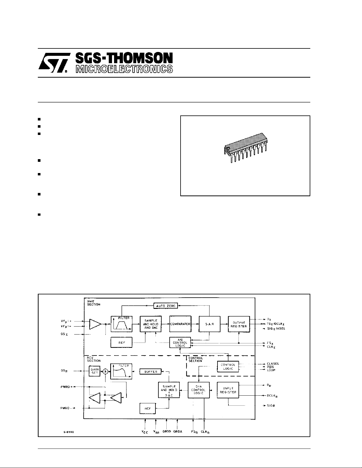
The M5913 is fully integrated PCM (pulse code
modulation)codecs and transmit/receivefilter using CMOS silicon gate technology.
The primary applications for the M5913 are telephone systems :
- Switching - M5913-Digital PBX’s and Central
M5913
DIP 20
ORDERING NUMBER: M5913B1
Office Switching Systems
- Concentration- M5913 SubscriberCarrier and
Concentrators.
The wide dynamic range (78dB) and the minimal
conversion time make it ideal products for other
applicationssuchas:
- Voice Store and Forward
- SecureCommunicationsSystems
- Digital Echo Cancellers
- SatelliteEarth Stations.
BLOCK DIAGRAM
December 1993
This is advanced information on a new productnow in development or undergoing evaluation. Details are subject to change without notice.
1/17
Page 2
M5913
ABSOLUTE MAXIMUM RATINGS
Symbol Parameter Value Unit
V
CC
V
BB
GRDD, GRDA In Such Case : 0 ≤ V
V
I/O
V
O DIG
P
tot
T
stg
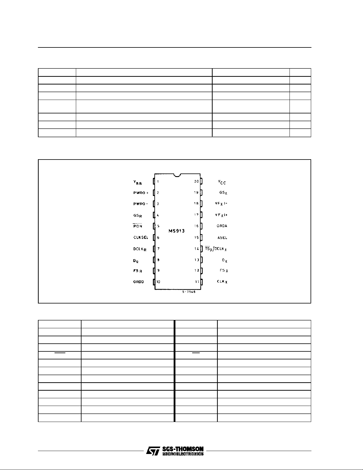
PIN CONNECTION(Top view)
With Respect GRDD, GRDA = 0V – 0.6 to 7 V
With Respect GRDD, GRDA = 0V -0.6 to – 7 V
≤ + 7V, – 7V ≤ VBB≤ 0V ± 0.3 V
CC
Analog Inputs, Analog Outputs and Digital Inputs VBB – 0.3 ≤ VIN/V
OUT
≤ VCC+
0.3
Digital Outputs GRDD – 0.3 ≤ V
≤ VCC+ 0.3 V
OUT
TotalPower Dissipation 1 W
Storage Temperature Range -65 to 150 °C
V
PIN NAMES
Symbol Parameter Symbol Parameter
V
BB
PWRO+, PWRO- Power Amplifier Outputs VF
GS
R
Power (-5V) GS
X
I-, VFXI+ Analog Inputs
X
Gain Setting Input for receive Channel GRDA Analog Ground
PDN Power Pown Select NC No Connected
CLKSEL Master Clock Select SIG
X
LOOP Analog Loop Back ASEL µ or A-law Select
SIG
R
DCLK
R
D
R
FS
R
GRDD Digital Ground CLK
V
CC
SignalingBit Output TS
Receive Data Rate Clock DCLK
Receive Channel Input D
X
X
X
Receive Frame Synchronization Clock FSX Transmit Frame Synchronization Clock
X Transmit Master Clock
Power (+5V) CLK
R
2/17
Gain Control
Transmit Digital Signaling Input
Digital Output - Timeslot Strobe
Transmit Data Rate Clock
Transmit (Digital) Output
Receive Master Clock
Page 3
PIN DESCRIPTION
Symbol Function
V
BB
PWRO+ Non-inverting Output of Power Amplifier. Can drive transformer hybrids or high impedance loads
PWRO - Inverting Output of Power Amplifier. Functionally identical and complementary to PWRO+.
GS
R
PDN Power Down Select. When PDN is TTL high, the device is active.When low, the device is powered
CLKSEL input which must be pinstrapped to reflect the master clock frequency at CLK
LOOP Analog Loopback. When this pin is TTL high, the receive output (PWRO+)is internally connected
SIG
R
DCLK
R
D
R
FS
R
GRDD Digital Ground for all Internal Logic Circuits. Not internally tied to GRDA.
CLK
R
CLK
X
FS
X
D
X
TS
/DCLK
X
SIG
/ASEL A dual purpose selects µ-law and pin. When connected to VBB. A law operation is selected. When it
X
NC Not Connected.
GRDA Analog ground return for all internal voice circuits.Not internally connected to GRDD.
I+ Non inverting analog input to uncommitted transmit operational amplifier.
VF
X
I- Invertinganalog input to uncommitted transmit operational amplifier.
VF
X
GS
X
V
CC
Most Negative Supply. Input voltage is -5 volts ±5%.
directly in either a differentialor single ended configuration.
Input to the gain Setting Network on the Output Power Amplifier, Transmission level can be
adjusted over a 12dB range depending on the voltage at GS
.
R
down.
, CLKR.
CLKSEL = V
BB
2.048MHz
X
CLKSEL = GRDD 1.544MHz
CLKSEL = V
to VF
CC
I+, GSRis internally connected to PWRO-, and VFXI- is internally connected to GSX.
X
A 0dBm0 digital signal input at D
1.536MHz
is returned as a +3dBm0 digital signal output at DX.
R
Signalling Bit Output, Receive Channel. In fixed data rate mode. SIGRoutputs the logical state of
the eighth bit of the PCM wordin the most recent signaling frame.
Selects the fixed or variable data rate mode. When DCLKR is connected to VBB, the fixed data rate
mode is selected.
When DCLK
mode DCLK
is not connected to VBB, the device operates in the variable data rate mode. In this
R
becomes the receive data clock wich operates at TTL levels from 64kB to 4.096MB
R
data rates
Receive PCM Input. PCM data is clocked in on this lead on eight consecutive negative transitions
of the receive data clock: CLKR inthe fixed data rate mode and DCLK
in variable data rate mode.
R
8kHz frame synchronization clock input/timeslot enable, receive channel. A multifunction input
which in fixed data rate mode distinguishes between signaling and non-signaling frames by means
of a double or single wide pulse respectively. In variable data rate mode this signal must remain
high for the entire length of the timeslot. The receive channel enters the standby state whenever
FSR is TTL low for 30 miliseconds
Receive master and data clock for the fixed data rate mode; receive master clock only in variable
data rate mode.
Transmit master anddata clock for the fixed data rate mode; transmit master clock only in variable
data rate mode.
8kHz frame synchronization clock input/timeslot enable, transmit channel. Operates independently
but in an analogous manner to FSR. The transmit channel enters the standby state whenever FS
is TTL low for 30 milliseconds.
Transmit PCM Output. PCM data is clocked out on this lead on eightconsecutive positive
transitionsof the transmit data clock : CLK in fixed datarate modeand DCLK
invariable datarate
X
mode.
Transmit channel timeslot strobe (output) or data clock (input) for the transmit channel. In fixed
X
data rate mode, this pin becomes the transmit data clock which operates at TTL levels from 64kB
to 4.096MB datarates.
is not connected to V
the eighth bit of the PCM wordduring signaling frames on the D
pin is a TTL level input for signaling operation. This input is transmitted as
BB
X
lead.
Output terminal of on-chip uncommitted op amp. Internally, this is the voice signal input to the
transmit filter.
Most positive supply ; input voltage is + 5 volts ±5%
M5913
X
3/17
Page 4

M5913
FUNCTIONAL DESCRIPTION
The M5913 provides the analog-to-digitaland the
digital-to-analogconversion and the transmit and
receive filtering necessary to interface a full duplex (4 wires) voice telephone circuit with the
PCM highway of a time division multiplexed
(TDM) system. It is intended to be used at the
analogterminationof a PCM line.
The following major functions are provided :
Bandpass filtering of the analog signals prior to
encodingand afterdecoding
Encoding and decoding of voice and call progressinformation
Encoding and decoding of the signaling and
supervisioninformation
GENERALOPERATION
SystemReliability Features
The combo-chip can be powered up by pulsing
FS
and/or FSRwhile a TTL high voltage is ap-
X
plied to PDN, provided that all clocks and supplies are connected. The M5913 has internal resets on power up (or when V
or VCCare
BB
re-applied)in order to ensure validity of the digital
outputs and thereby maintain integrity of the PCM
highway.
On the transmit channel, digital outputs D
are held in a high impedance state for ap-
TS
X
proximatelyfour frames(500µs) after power up or
application of V
TS
will be functional and will occur in the proper
X
timeslot. The analog circuits on the transmit side
or VCC. After this delay, DXand
BB
X
and
require approximately 40 milliseconds to reach
their equilibrium value due to the autozero circuit
setting time. Thus, valid digital information, such
as for on/off hook detection, is available almost
immediately,while analog information is available
aftersome delay.
On the receive channel, the digital output SIG
R
also held low for a maximum of four frames after
power up or application of V
or VCC, SIGRwill
BB
remain low thereafter until it is updated by a signalingframe.
To furtherenhance systemreliability, TS
will be placed in a high impedance state approximately 20µs after an interruption of CLK
and D
X
. Simi-
X
Table 1: PowerDown Methods
larly SIG
ter an interruption of CLK
will be held low approximately 20µs af-
R
These interruptions
R.
could possibly occur with some kind of fault condition.
PowerDown And Standby Modes
To minimizepower consumption,two power down
modes are provided in which most M5913 functions are disabled. Only the power down, clock,
and frame sync buffers, which are required to
powerup the device, are enabled in thesemodes.
Asshown in table 1, the digital outputs on the appropriate channels are placed in a high impedance state until the device returns to the active
mode.
The Power Down mode utilizes an external control signal to the PDN pin. In this mode, power
consumptionis reduced to an average of 0.5mW.
The device is active when the signal is high and
inactive when it is low. In the absence of any signal, the PDN pin floats to TTL high allowing the
deviceto remain active continuously.
The Standby mode leaves the user an option of
powering either channel down separately or powering the entire down by selectivelyremoving FS
and/or FSR. With both channels in the standby
state, power consumptionis reduced to an average of 1mW. If transmit only operation is desired,
should be applied to the device while FSRis
FS
X
held low. Similarly, if receiveonly operation is desired, FS
should be applied while FSXis held
R
low.
Fixed Data Rate Mode
Fixed data rate timing, is selected by connecting
DCLK
CLK
FS
CLK
is
to operate the codec and filter sections and bit
to VBB. It employs master clock CLKX,and
R
, frame synchronization clocks FSXand
R
, and outputTSX.
R
, and CLKR, serve both as the master clock
X
clocks to clock the data in and out from the PCM
highway. FS
andFSRare 8kHz inputs which set
X
the sampling frequency and distinguish between
signaling and non-signaling frames by thir pulse
X
width.A frame synchronizationpulse which is one
master clock wide designates a non-signaling
frame, while a double wide sync pulse enables
X
Device Status Power Down Methods Digital Outputs Status
Power Down Mode PDN = TTL low TS
Stand-by Mode FS
Only transmit is on stand-by FS
Only receive is on stand-by FS
4/17
and FSRare TTL low TSXand DXare placed in a high impedance state and
X
is TTL low TSXand DXare placed in a high impedance state
X
is TTL low SIGRis placed in a TTL low state within 30ms.
R
and DXare placed in a high impedance state and
X
SIG
isplaced in a TTL low state within 10µs.
R
SIG
is placed in a TTL low state 30ms after FSXand
R
FS
are removed.
R
within 30ms.
Page 5

M5913
the signaling function. TSXis a timeslot
strobe/bufferenable output which gates the PCM
word onto the PCM highway when an external
buffer is used to drive the line.
Data is transmitted on the highway at D
first eight positive transitions of CLK
the rising edge of FS
. Similarly, on the receive
X
on the
X
following
X
side, data is received on the first eight falling
edgesof CLK
. Thefrequencyof CLKXand CLK
R
is selected by the CLKSEL pin to be either 1.536,
1.544 or 2.048MHz. No other frequency of operationis allowed in the fixed data rate mode.
VariableData Rate Mode
Variable data rate timing is selected by connecting DCLK
highway rather than to V
clocks CLK
DCLK
to the bit clock for the receive PCM
R
and CLKR, bit clocks DCLKRand
X
and frame synchronization clocks FS
X
. It employes master
BB
and FSX.
Variable data rate timing allows for a flexible data
frequency. It provides the ability to vary the frequency of the bit clocks, from 64kHz to 4096MHz.
Master clocks inputs are still restricted to 1.536,
1.544, or 2.048MHz.
In this mode, DCLK
and DCLKXbecome the
R
data clocks for the receive and transmit PCM
highways. While FS
is high, PCM data from D
X
is transmitted onto the highway on the next eight
consecutive positive transitions of DCLK
larly, while FS
highway is received by D
is high, each PCM bit from the
R
on the next eight con-
R
secutivenegativetransitions of DCLK
. Simi-
X
.
R
On the transmit side, the PCM word will be repeated in all remaining timeslots in the 125µs
frame as long as DCLK
is pulsed and FSXis
X
held high. This featureallows the PCM word to be
transmitted to the PCM highway more than once
per frame, if desired, and is only available in the
variable data rate mode. Conversely, signaling is
only allowed in the fixed data rate mode since the
variable mode provides no means with which to
specifya signaling frame.
PrecisionVoltageReferences
No external components are required with the
combochip to provide the voltage reference function. Voltage references are generated on-chip
and are calibrated during the manufacturing process. The technique use the bandgap principle to
derive a temperature and bias stable reference
voltage.These references determinethe gain and
dynamicrange characteristicsof the device.
Separate references are supplied to the transmit
and receive sections. Transmit and receive section are trimmed independentlyin the filter stages
to a final precision value. With this method the
combochip can achieve manufacturingtolerances
of typically ± 0.04dB in absolutegain for each half
channel, providing the user a significant margin
for error in other board components.
ConversionLaws
The M5913 is designed to operate in both µ-law
and A-law systems. The user can select either
conversion law according to the voltage present
on the SIG
R
and decoder process a companded 8-bit PCM
/ASEL pin . In each case the coder
X
word following CCITT recommandation G.711 for
µ-law and A-law conversion. If A-law operation is
desired, SIG
should be tied to VBB. Thus, signal-
X
ing is not allowed during A-law operation. If µ =
255-lawoperation is selected,then SIG
level input which modifies the LSB on the PCM
output in signaling frames
TRANSMIT OPERATION
R
Transmit Filter
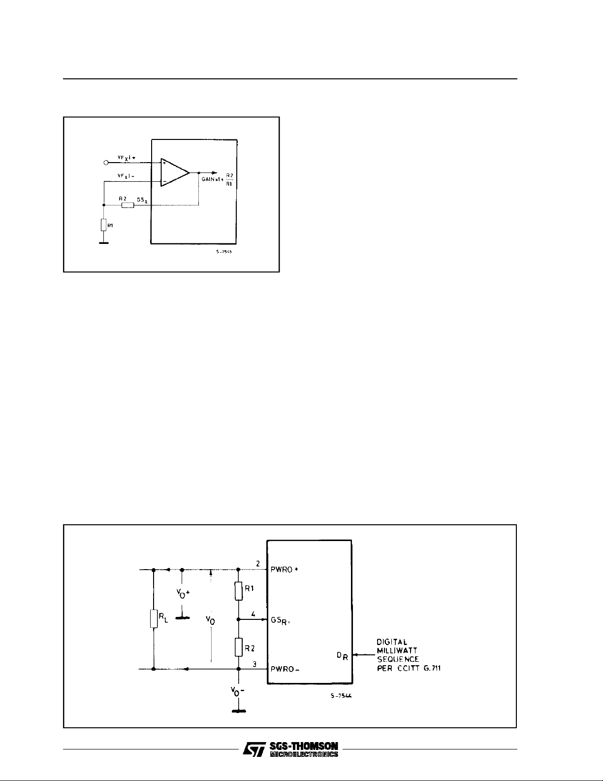
The input section provides gain adjustment in the
passband by means of an on-chip uncommitted
operational amplifier. This operational amplifier
has a commonmode range of 2.17V,a maximum
DC offset of 25mV, a minimum voltage gain of
5000, and a unity gain bandwidth of typically
1MHz. Gain of up to 20dB can be set without degrading the performance of the filter. The load im-
X
pedanceto ground (GRDA)at the amplifier output
) must be greater than 10kΩ in parallel high
(GS
X
less than 50pF. The input signal on lead VF
can be either AC or DC coupled. The input op
amp can also be used in the inverting mode or
differentialamplifiermode (see figure 3).
A low pass anti-aliasing section is included onchip. This section typically provides 35dB attenuation at the sampling frequency. No external components are required to provide the necessary
anti-aliasing function for the switched capacitor
sectionof the transmit filter.
Thepassband section provides flatness and stopband attenuation which fulfills the AT&T D3/D4
channel bank transmission specification and
CCITTrecommendation G.712.
The M5913 specifications meet or exceed digital
class 5 central office switching systems requirements. The transmit filter transfer characteristics
and specifications will be within the limits shown
the relative table.
A high pass section configuration was chosen to
reject low frequency noise from 50 and 60Hz
power lines, 17Hz European electric railroads,
ringing frequencies and their harmonics, and
otherlow frequencynoise.
Even though there is high rejection at these frequencies, the sharpness of the band edge gives
low attenuation at 200Hz. This feature allows the
use of low-cost transformer hybrids without external components.
is a TTL
X
I+
X
5/17
Page 6
M5913
Figure3: Transmit Filter Gain Adjustment.
Encoding
The encoder internally samples the output of the
transmit filter and holds each sample on an internal sample and hold capacitor.
The encoder then performs an analog to digital
conversion on a switched capacitor array. Digital
data representing the sample is transmitted on
the first eight data clockbits of thenext frame.
An on-chip autozero circuit corrects for DC-offset
on the input signal to the encoder. This autozero
circuit uses the sign bit averaging technique. In
this way, all DC offset is removed from the encoderinput waveform.
RECEIVEOPERATION
Decoding
The PCM word at the D
lead is serially fetched
R
on the first eight data clockbits of the frame.
A D/A conversion is performed on the digital word
and the corresponding analog sample is held on
Figure4: Gain Setting Configuration.
an internal sample and hold capacitor. This sample is then transferredto the receive filter.
ReceiveFilter
The receive section of the filter provides passband flatness and stopband rejection which fulfills
both the AT&T D3/D4 specification and CCITT
recommendationG.712. The filter contains the required compensation for the (sin X)/X response of
such decoders. The receive filter characteristics
and specificationsare shown in the relative table.
ReceiveOutput PowerAmplifiers
A balancedoutput amplifier is provided in order to
allow maximum flexibility in output configuration.
Either of the two outputs can be used single
ended (referenced to GRDA) to drive single
ended loads. Alternatively, the differential output
will drive a bridged load directly. The output stage
is capable of driving loads as low as 300 ohms
singleended to a levelof 12dBmor 600 ohms differentiallyto a levelof 15dBm.
The receive channel transmission level may be
adjusted between specified limits by manipulation
of the GS
an analog gain setting network. When GS
input. GSRis internally connected to
R
is
R
strapped to PWRO–, the receive level is minimized;when it is tied to PWRO+, the level is minimized. The output transmission level interpolates
between 0 and -12dB as GSR is interpolated
(with potentiometer) between PWRO- and
PWRO+. The use of the output gain set is illustratedin figure 4.
Transmission levels are specified relative to the
receive channel output under digital milliwatt conditions, that is, when the digital input at D
R
is the
eight-code sequence specified in CCITT recommendationG.711.
6/17
Page 7
M5913
OUTPUT GAIN SET: DESIGN CONSIDERATIONS (refer to figure 4)
PWRO+and PWRO–are low impedancecomplementaryoutputs. Thevoltages at the nodes are:
V
at PWRO+
O
V
at PWRO
O
V
O=VO+VO
– (total differentialresponse)
R1 and R2 are a gain setting resistornetwork with
the center tap connected to the GS
input. A
R
whereA =
For design purposes, a useful form is R1/R2 as a
functionof A.
(allowable values for A are those which make
R1/R2positive)
V
=AV
O
1 +(R
4+(R
R1 /R2 =
A
4A –
1 –A
1/R2
1/R2
1
)
)
value greater than 10KΩ andless than 100KΩ for
R1 + R2 is recommended because:
a) The parallel combination of R1 + R2 and RL
sets the total loading.
b) The total capacitanceat the GS
input and the
R
parallel combination of R1 and R2 define a
time constant which has to be minimized to
avoid inaccuracies.
If VA represents the output voltage without any
gain setting networkconnected, you can have:
DC CHARACTERISTICS (T
erwise specified)Typicalvalues are for T
Symbol Parameter Test Conditions Min. Typ. Max. Unit
DIGITAL INTERFACE
I
I
V
V
V
V
V
V
V
C
C
Low LevelInput Current GRDD ≤ VIN≤ VIL(note 1) 10 µA
IL
High Level Input Current VIH≤ VIN≤ V
IH
Input Low Voltage, Except CLKSEL 0.8 V
IL
Input High Voltage, Except CLKSEL 2.0 V
IH
Output Low Voltage IOL= 3.2mA at DX,TSXand
OL
Output High Voltage IOH= 9.6mA at D
OH
Input Low Voltage, CLKSEL (note 2) V
ILO
Input Intermediate Voltage, CLKSEL GRDD
IIO
Input High Voltage, CLKSEL VCC-
IHO
Digital Output Capacitance (note 3) 5 pF
OX
Digital Input Capacitance 5 10 pF
IN
= 0 to 70oC, VCC= +5V ± 5%,VBB=–5V±5%, GRDA= 0V,unlessoth-
amb
=25oC and nominal power supply values.
amb
Examplesare:
If A = 1 (maximum output), then
R1/R2 = ∞ or V(GS
i.e., GS
istied to PWRO+
R
If A = 1/2. then
R1/R2 = 2
If A = 1/4 (minimum output) then
R1/R2 = 0 or V(GS
i.e., GSR is tied to PWRO+
CC
SIG
R
IOH= 1.2mA at SIG
X
R
)=VO;
R
)=VO+;
R
10 µA
0.4 V
2.4 V
BB
-0.5
0.5
VBB+
0.5
0.5 V
VCC V
V
Notes:
is the voltage on any digital pin.
1. V
IN
and DCLKRareTTL level inputs between GRDD and VCC; theyare also pinstraps for mode selection when tied to VBB.
2. SIG
X
Underthese conditions V
3. Timing parameters are guaranteed based on a 100pF load capacitance.
Upto eight digitaloutputs may be connected to a common PCM highway without buffering,assuming a board capacitance of 60pF.
is the input low voltage requirement.
ILO
7/17
Page 8

M5913
DCCHARACTERISTICS (continued)
Symbol Parameter Test Conditions Min. Typ. Max Unit
POWER DISSIPATION All measurements made at f
I
I
I
I
I
CCS
I
P
P
P
CC1
BB1
CC0
BB0
BBS
VCCOperating Current 6 10 mA
VBBOperating Current 6 9 mA
VCCPower Down Current PDN ≤ VIL; after 10µs 40 300 µA
VBBPower Down Current PDN ≤ VIL; after 10µs 40 300 µA
VCCStandby Current FSX,FSR≤VIL; after 30ms 300 600 µA
VBBStandby Current FSX,FSR≤VIL; after 30ms 40 300 µA
Operating Power Dissipation 60 100 mW
D1
Power Down Dissipation PDN ≤ VIL; after 10µs 0.4 3 mW
D0
Standby Power Dissipation FSX, FSR≤ VIL; after 30ms 1.7 5 mW
ST
ANALOG INTERFACE, RECEIVE FILTER DRIVER AMPLIFIER STAGE
I
BX1
R
V
OSXI
CMRR Common Mode Rejection, VF
A
VOL
f
V
C
R
Input Leakage Current, VFXI+, VFXI- -2.17V ≤ VIN≤ 2.17V 100 nA
Input Resistance, VFXI+, VFXI- 10 MΩ
IXI
Input OffsetVoltage, VFXI+, VFXI- 25 mV
I+, VFXI- -2.17V ≤ VIN≤ 2.17V 55 dB
X
DC Open Loop Voltage Gain, GS
Open Loop Unity Gain Bandwidth, GS
C
Output Voltage Swing GS
OXI
Load Capacitance, GS
LXI
Minimum Load Resistance, GS
LXI
X
X
X
X
ANALOG INTERFACE, RECEIVE FILTER DRIVER AMPLIFIER STAGE
R
V
ORA
OSRA
Output Resistance, PWRO+, PWRO- 1 Ω
Single-ended Output DC Offset,
PWRO+, PWRO-
C
Load Capacitance, PWRO+, PWRO- 100 pF
LRA
= 2.048MHz, outputsunloaded
DCLK
RL= 10K 5000 20.000
X
1MHz
RL≥ 10kΩ – 2.17 2.17 V
10 kΩ
Relative to GRDA -150 75 150 mV
50 pF
ACCHARACTERISTICS - TRANSMISSIONPARAMETERS
Unless otherwie noted, the analog input is a 0dBm0, 1020Hz sine wave
1
. Input amplifier is set for unity
gain, noninverting. The digital inputs is a PCM bit stream generated by passing a 0dBm0, 1020Hz sine
wave through an ideal encoder. Receive output is measured singleended, maximum gain configuration
Alloutput levelsare (sinX)/X corrected.
Symbol Parameter Test Conditions Min. Typ. Max. Unit
GAIN AND DYNAMIC RANGE
EmW Encoder MilliwattResponse
(transmit gain tolerance)
EmW
EmW Variation with Temperature and
TS
Supplies
DmW Digital Milliwatt Response
(receive gain tolerance)
DmW
DmW Variation with Temperature and
TS
Supplies
0TLP
Zero Transmission Level Point
1X
Transmit Channel (0dBm0) µ-law
0TLP
Zero Transmission Level Point
2X
Transmit Channel (0dBm0) A-law
0TLP
Zero Receive Level Point
1R
Receive Channel (0dBm0) µ-law
0TLP
Zero Transmission Level Point
2R
Transmit Channel (0dBm0)) A-law
8/17
=25°C, VBB= – 5V,
T
amb
V
=+5V
CC
± 5% Supplies, 0 to 70°C
-0.15 ± 0.04 +0.15 dBm0
-0.12 +0.12 dB
Relative to Nominal
Conditions
T
=25°C;VBB= – 5V,
amb
V
=+5V
CC
-0.15 ± 0.04 +0.15 dBm0
± 5%, 0 to70°C -0.08 +0.08 dB
Referenced to 600Ω
Referenced to 900Ω
Referenced to 600Ω
Referenced to 900Ω
Referenced to 600Ω
Referenced to 900Ω
Referenced to 600Ω
Referenced to 900Ω
+ 2.76
+ 1.00
+ 2.79
+ 1.03
+ 5.76
+ 4.00
+ 5.79
+ 4.03
dBm
dBm
dBm
dBm
dBm
dBm
dBm
dBm
2
.
Page 9

M5913
ACCHARACTERISTICS (continued)
Symbol Parameter Test Conditions Min. Typ. Max. Unit
GAIN TRACKING Reference Level = – 10dBm0
GT1
Transmit Gain Tracking Error
X
Sinusoidal Input; µ-law
GT2
Transmit Gain Tracking Error
X
Sinusoidal Input; A-law
GT1
Receive GainTracking Error
R
Sinusoidal Input; µ-law
GT2
Receive GainTracking Error
R
Sinusoidal Input; A-law
NOISE
N
N
Transmit Noise, C-message Weighted VFXI+ = GRDA,VFXI– = GS
XC1
Transmit Noise, C-message
XC2
Weighted with Eighth Bit Signaling
N
Transmit Noise, Psophometrically
XP
Weighted
N
Receive Noise, C-message Weighted:
RC1
Quiet Code
N
Receive Noise, C-message Weighted:
RC2
Sign Bit Toggle
N
Receive Noise, Psophometrically
RP
Weighted
N
Single Frequency NOISE End to End
SF
Measurement
PSRR
1VCC
Power Supply Rejection, Transmit
Channel
PSRR
2VBB
Power Supply Rejection, Transmit
Channel
PSRR
3VCC
Power Supply Rejection, Receive
Channel
PSRR
4VBB
Power Supply, Rejection Receive
Channel
CT
Crosstalk, Transmit to Receive,
TR
Single Ended Outputs
CT
Crosstalk, Receive to Transmit,
RT
Single Ended Outputs
Notes:
1. 0dBm0 is defined as the zero reference point of the channel under test (0TLP). This corresponds to an analogsignal input of 1.064 V
or anoutput of 1.503 V
2. Unity gain input amplifier : GS
outputto PWRO+.
3. Noise free:DX PCM Code stable at 01010101.
(µLaw) dual 1.068 V
rmst
isconnected to VFXI, Signal input VFXI+; Maximum gain output amplifier: GSRis connected to PWRO,
X
or a output 1.516 V
rmst
+ 3 to – 40dBm0
– 40 to – 50dBm0
– 50 to – 55dBm0
+ 3 to – 40dBm0
– 40 to – 50dBm0
– 50 to – 55dBm0
+ 3 to – 40dBm0
– 40 to – 50dBm0
– 50 to – 55dBm0
+ 3 to – 40dBm0
– 40 to – 50dBm0
– 50 to – 55dBm0
VFXI+ = GRDA, VFXI– = GS
X
X
± 0.2
± 0.4
± 1.0
± 0.2
± 0.4
± 1.0
± 0.2
± 0.4
± 1.0
± 0.2
± 0.4
± 1.0
0 13 dBrnc0
13 18 dBrnc0
6 th Frame Signaling
VFXI+ = GRDA, VFXI– = GS
DR= 11111111 Measure at
X
(note3) – 80 dBrnc0
1 9 dBrnc0
PWRO+
Input to DRis 0 code with
1 10 dBm0p
Sign Bit Toggle at 1KHz Rate
DR= Lowest Positive Decode
-90 – 81 dB0p
Level
CCITT G.712.4.2 – 50 dBm0
Idle Channel ; 200mV P-P
–40 dB
Signal on Supply ; 0 to
50kHz, Measure at D
Idle Channel ; 200mV P-P
X
–40 dB
Signal on Supply ; 0 to
50kHz, Measure at D
Idle Channel ; 200mV P-P
X
–40 dB
Signal on Supply ; Measure
Narrow Band at PWRO+
Single Ended, 0 to 50kHz
Idle Channel ; 200mV P-P
–40 dB
Signal on Supply ; Measure
Narrow Band at PWRO+
Single Ended, 0 to 50kHz
VFXI+ = 0dBm0, 1.02kHz,
D
= Lowest Positive Decode
R
–80 dB
Level, Measure at PWRO+
DB= 0dBm0, 1.02kHz,
VF
I+ = GRDA, Measure at
X
D
X
(A-Law)
rmst
–80 dB
dB
dB
dB
dB
dB
dB
dB
dB
dB
dB
dB
dB
rms
9/17
Page 10

M5913
A.C. CHARACTERISTICS (continued)
Symbol Parameter Test Conditions Min. Typ. Max. Unit
DISTORTION
SD1
Transmit Signal to Distortion, µ-law
X
Sinusoidal Input;
CCITT G.712-method 2
SD2
Transmit Signal to Distortion, A-law
X
Sinusoidal Input,
CCITT G.712-method 2
SD1RTransmit Signal to Distortion,
µ-law Sinusoidal Input ,
CCITT G.712-method 2
SD2RReceive Signal to Distortion, A-law
Sinusoidal Input;
CCITT G.712-method 2
DP
Transmit Single Frequency Distortion
X1
Products
DP
Receive Single Frequency Distortion
R1
Products
IMD
Intermodulation Distortion,
1
End to End Measurement
IMD
Intermodulation Distortion,
2
End to End Measurement
SOS Spurious Out of Band Signals,
End to End Measurement
SIS Spurious in Band Signals,
End to End Measurement
D
D
D
D
Transmit Absolute Delay Fixed Data Rate CLKX=
AX
Transmit DifferentialEnvelope Delay
DX
Relative to D
Receive Absolute Delay Fixed data rate, CLKR=
AR
Receive Differential Envelope Delay
DR
Relative to D
AX
AR
0 ≤ VF
I+ ≤ – 30dBm0
X
– 40dBm0
– 45dBm0
0 ≤ VFXI+ ≤ – 30dBm0
– 40dBm0
– 45dBm0
0 ≤ VFXI+ ≤ – 30dBm0
– 40dBm0
– 45dBm0
0 ≤ VF
I+ ≤ – 30dBm0
X
– 40dBm0
– 45dBm0
AT & T Adivisory # 64 (3.8)
0dBm0 Input Signal
AT & T Adivisory # 64 (3.8)
0dBm0 Input Signal
CCITT G.712 (7.1) – 35 dB
CCITT G.712 (7.2) – 49 dB
CCITT G.712 (6.1) – 30 dBm0
CCITT G.712 (9) – 40 dBm0
2.048MHz,
0dBm0, 1.02kHz Signal at
VF
I+ Measure at D
X
X
f = 500 – 600Hz
f = 600 – 1000Hz
f = 1000– 2600Hz
f = 2600– 2800Hz
2.048MHz;
Digital input is DMW codes.
Measure at PWRO+
f = 500 – 600Hz
f = 600 – 1000Hz
f = 1000– 2600Hz
f = 2600– 2800Hz
36
30
25
36
30
25
36
30
25
36
30
25
–46 dB
–46 dB
300 µs
170
95
45
80
190 µs
10
10
85
110
dB
dB
dB
dB
dB
dB
dB
dB
dB
dB
dB
dB
µs
µs
µs
µs
µs
µs
µs
µs
10/17
Page 11

M5913
A.C.CHARACTERISTICS (continued)
TRANSMIT CHANNEL TRANSFER CHARACTERISTICS
(Inputamplifier is set for unity gain, noninverting;maximum gain output.)
Symbol Parameter Test Conditions Min. Typ. Max. Unit
G
Figure5: Transmit Filter
Gain Relative to Gain at 1.02 kHz 0 dBm0 Signal Input at VFXI+
RX
16.67Hz –30 dB
50Hz –25 dB
60Hz –23 dB
200Hz – 1.8 – 0.125 dB
300 to 3000Hz – 0.125 + 0.125 dB
3300Hz – 0.35 + 0.03 dB
3400Hz – 0.7 – 0.10 dB
4000Hz –14 dB
4600Hz and Above –32 dB
11/17
Page 12

M5913
A.C.CHARACTERISTICS (continued)
RECEIVECHANNEL TRANSFER CHARACTERISTICS
Symbol Parameter Test Conditions Min. Typ. Max. Unit
G
Figure6: ReceiveFilter
Gain Relative to Gainat 1.02kHz 0dBm0 Signal Input at D
RR
below200Hz + 0.125 dB
200Hz – 0.5 + 0.125 dB
300 to 3000Hz – 0.125 + 0.125 dB
3300Hz – 0.35 + 0.03 dB
3400Hz – 0.7 – 0.1 dB
4000Hz –14 dB
4600Hz and Above –30 dB
R
12/17
Page 13

M5913
AC CHARACTERISTICS - TIMINGPARAMETERS
Symbol Parameter Test Conditions Min. Typ. Max. Unit
CLOCK SECTION
t
t
CLK
t
DCLK
t
CDC
t
r,tf
Clock Period, CLKX, CLK
CY
Clock Pulse Width CLKX,CLK
Data Clock Pulse Width
R
1
Clock Duty Cycle CLKX,CLK
Clock Rise and Fall Time 5 30 ns
TRANSMIT SECTION, FIXED DATA RATE MODE
t
DZX
t
DDX
t
HZX
t
SON
t
SOFF
t
FSD
t
t
Data Enabled on TS Entry 0 < C
Data Delay from CLK
X
Data Float on TS Exit C
Timeslot X to Enable 0 < C
Timeslot X to Disable C
Frame Sync Delay 0 120 ns
Signal Setup Time 0 ns
SS
Signal Setup Time 0 ns
SH
RECEIVE SECTION, FIXED DATA RATE MODE
t
DSR
t
DHR
t
FSD
t
SIGR
Receive Data Setup 10 ns
Receive Data Hold 60 ns
Frame Sync Delay 0 120 ns
SIGRUpdate 0 2 µs
TRANSMIT SECTION, FIXED DATA RATE MODE
t
TSDX
t
FSD
t
DDX
t
DON
t
DOFF
f
t
DFSX
Timeslot Delay from DCLK
X
Frame Sync Delay 0 120 ns
Data Delay from DCLK
X
Timeslot to DXActive 0 < C
Timeslot to DXInactive 0 < C
Data Clock Frequency 64 20481KHz
DX
Data Delay from FS
X
RECEIVE SECTION, FIXED DATA RATE MODE
t
TSDR
t
FSD
t
DSR
t
DHR
t
DR
t
SER
Timeslot Delay from DCLK
R
Frame Sync Delay 0 120 ns
Receive Data Setup Time 10 ns
Receive Data HoldTime 60 ns
Data Clock Frequency 64 20481kHz
Timeslot End Receive Time 0 ns
64KB OPERATION, VARIABLE DATA RATE MODE
t
FSLX
Transmit Frame Sync Minimum
Downtime
t
FSLR
Receive Frame Sync Miniumum
Downtime
t
DCLK
Notes:
1. Devices are available wich operate at data rates up to 4.096MHz; the minimum data clock pulse width for these devices is 110ns
2. Timing parameters t
Data Clock Pulse Width 10 µs
DZX,tHZX
,and t
are referenced to a high impedance state.
SOFF
f
CLKX=fCLKR
64kHz ≤ f
2
0<C
LOAD
LOAD
2
= 2.048MHz 488 ns
R
≤ 2.048MHz 195 ns
DCLK
R
< 100pF 0 145 ns
LOAD
< 100pF 0 145 ns
LOAD
195 ns
40 50 60 %
= 0 60 190 ns
< 100pF 0 145 ns
LOAD
= 0 50 190 ns
-80 80 ns
0 < CLOAD < 100pF 0 100 ns
< 100pF 0 50 ns
LOAD
< 100pF 0 80 ns
LOAD
t
= 80ns 0 140 ns
TSDX
-80 80 ns
FSXis TTL high for
488 ns
remainder of frame
FSRis TTL high for
1952 ns
remainder of frame
13/17
Page 14

M5913
WAVEFORMS:
FixedData Rate Timing - Transmit Timing
NOTE: All timing parameters referenced to VIHand VILexcept t
ReceiveTiming
DZX,tSOFF
and t
which reference a high impedance state.
HZX
NOTE: All timing parameters referenced to V
14/17
IH
and V
IL
Page 15

VARIABLE DATA RATE TIMING
M5913
AC Timing Input, Output Waveform
15/17
Page 16

M5913
DIP20 PACKAGEMECHANICAL DATA
DIM.
MIN. TYP. MAX. MIN. TYP. MAX.
a1 0.254 0.010
B 1.39 1.65 0.055 0.065
b 0.45 0.018
b1 0.25 0.010
D 25.4 1.000
E 8.5 0.335
e 2.54 0.100
e3 22.86 0.900
F 7.1 0.280
I 3.93 0.155
L 3.3 0.130
Z 1.34 0.053
mm inch
16/17
Page 17

M5913
Information furnished is believed to be accurate and reliable. However, SGS-THOMSON Microelectronics assumes no responsibility for the
consequences of use of such information nor for any infringement of patents or otherrights of third parties which may result from its use. No
license is granted by implication or otherwise under any patent or patent rights of SGS-THOMSON Microelectronics. Specifications mentioned in this publication are subject to change without notice. This publication supersedes and replaces all information previously supplied.
SGS-THOMSON Microelectronics products are not authorized for use as critical components in life support devices or systems without express written approval of SGS-THOMSON Microelectronics.
1994 SGS-THOMSON Microelectronics - All RightsReserved
SGS-THOMSON Microelectronics GROUP OF COMPANIES
Australia - Brazil- France - Germany - Hong Kong - Italy - Japan - Korea -Malaysia - Malta - Morocco - The Netherlands - Singapore -
Spain - Sweden - Switzerland - Taiwan - Thaliand - United Kingdom - U.S.A.
17/17
 Loading...