

Page 1
32 Mbit (2Mb x16, Mux I/O, Dual Bank, Burst)
■ SUPPLY VOLTAGE
= V
–V
DD
Erase and Read
–V
= 12V for fast Program (optional)
PP
■ MULTIPLEXED ADDRESS/DATA
■ SYNCHRONOUS / ASYNCHRONOUS READ
– Burst mode Read: 40MHz
– Page mode Read (4 Words Page)
– Random Access: 100ns
■ PROGRAMMING TIME
– 10µs by Word typical
– Two or four words programming option
■ MEMORY BLOCKS
– Dual Bank Memory Array: 8/24 Mbit
– Parameter Blocks (Top or Bott o m location)
■ DUAL OPERATIONS
– Read within one Bank while Program or
Erase within the other
– No delay between Read and Write operations
■ PROTECTION/S ECURITY
– All Blocks protected at Power-up
– Any combination of Blocks can be protected
– 64 bit unique device identifier
– 64 bit user programmable OTP cells
– One parameter block permanently lockable
■ COMMON FLASH INTERFACE (CFI)
■ 100,000 PROGRAM/ERASE CYCL ES per
BLOCK
■ ELECTRONIC SIGNATURE
– Manufacturer Code: 20h
– Top Device Code, M58MR032C: 88DAh
– Bottom Device Code, M58MR032D: 88DBh
= 1.7V to 2.0V for Program,
DDQ
M58MR032C
M58MR032D
1.8V Supply Flash Memory
PRELIMINARY DATA
FBGA
TFBGA48 (ZC)
10 x 4 ball array
Figure 1. Logic Diagram
V
V
DDQVPP
DD
A16-A20
W
RP
WP
5
E
G
L
K
M58MR032C
M58MR032D
V
SS
16
ADQ0-ADQ15
WAIT
BINV
AI90019
August 2002
This is preliminary information on a new product now in development or undergoing evaluation. Details are subject to change without notice.
1/52
Page 2
M58MR032C, M58MR032D
Figure 2. TFBGA Connections (Top view through package)
87654321
A
B
C
D
E
F
G
H
DU
DU
DU
DU
DDQ
SS
NC
V
ADQ14ADQ15
SS
SS
KWAIT
ADQ13 ADQ12
DD
WV
WPRPBINVLA20A16V
ADQ2ADQ3ADQ6ADQ7V
ADQ10ADQ11ADQ4ADQ5V
V
109
A19
A18
DDQ
A17
ADQ8
ADQ1
PP
ADQ9
V
1211
DU
NC
V
E
SS
G
ADQ0
DU
1413
DU
DU
AI90020
DESCRIPTION
The M58MR032 is a 32 Mbit non-volatile Flash
memory that m ay be erased electrically a t block
level and programmed i n-system on a Word-byWord basis using a 1.7V to 2.0V V
supply for the
DD
circuitry. For Program and Erase operations the
necessary high voltages are gen erated internally.
The device supports synchronous burst read and
asynchronous read from all the blocks of the memory array; at power-up the device is configured for
page mode read. In sy nchronous burst mode, a
new data is output at each clock cycle for frequencies up to 40MHz.
The array matrix organization allows each block to
be erased and reprogrammed without affecting
other blocks. All blocks are protected against programming and erase at Power-up.
Blocks can be unprotected to make changes in the
application and then re-protected.
A parameter block "Security block" can be permanently protected against programming and erasing
2/52
in order to increase the data security. An optional
12V V
power supply is provided to speed up the
PP
program phase at costumer production. An internal command interface (C.I.) decode s the instructions to access/modify the memory content. The
program/erase controller (P/E.C.) automatically
executes the algorithms taking care of the timings
necessary for program and erase operations. Two
status registers indicate the state of each bank.
Instructions for Read Array, Read Electronic Signature, Read Status Register, Clear Status Register, Write Read Configuration Register, Program,
Block Erase, Bank Erase, Program Suspend, Program Resume, Erase Suspend, Erase Resume,
Block Protect, Block Unprotect, Block Locking,
Protection Program, CFI Query, are wri tten to t he
memory through a Command Interface (C.I.) using
standard micro-processor write timings.
The memory is offered in TFBGA48, 0. 5 mm ball
pitch packages and it is supplied with all the bits
erased (set to ’1’).
Page 3
M58MR032C, M58MR032D
Table 1. Signal Names
A16-A20 Address Inputs
ADQ0-ADQ15
Data Input/Outputs or Address
Inputs, Command Inputs
Organization
The M58MR032 is organized as 2Mb by 16 bits.
The first sixteen address lines are multiplexed with
the Data Input/Output signals on the m ultiplexed
address/data bus ADQ0-ADQ15. The remaining
address lines A16-A20 are the MSB addresses.
E
G
W
RP
Chip Enable
Output Enable
Write Enable
Reset/Power-down
Chip Enable E
W
inputs provide memory control.
, Output Enable G and Write Enable
The clock K input synchronizes the memory to the
microprocessor during burst read.
Reset RP
is used to reset all the memory circuitry
and to set the chip in power-down mode if a proper
setting of the Read Configuration Register en-
WP
K Burst Clock
L
Write Protect
Latch Enable
ables this function.
output indicates to t he microprocessor the
WAIT
status of the memory during the burst mode operations.
Memory Blocks
WAIT
BINV Bus Invert
V
DD
V
DDQ
V
PP
Wait Data in Burst Mode
Supply Voltage
Supply Voltage for Input/Output
Buffers
Optional Supply Voltage for
Fast Program & Erase
The device features asymmetrically blocked architecture. M58MR032 has an array of 71 blocks and
is divided into two banks A and B, prov iding D ual
Bank operations. While programming or erasing in
Bank A, read operations are possible into Bank B
or vice versa. Only one bank at the time is allowed
to be in program or erase mode. It is possible to
perform burst reads that cross bank boundaries.
The memory features an eras e suspend allowing
reading or programming in another block. Once
suspended the erase can be resumed. Program
V
SS
Ground
can be suspended to read data in another block
and then resumed. The Bank S ize and sectoriza-
DU Don’t Use as Internally Connected
NC Not Connected Internally
tion are summarized in Table 3. Parameter Blocks
are located at the top of the memory address
space for the M58MR032C, and at the bottom for
the M58MR032D. The memory maps are shown in
Figure 3.
Table 2. Absolute Maximum Ratings
Symbol Parameter Value Unit
T
A
T
BIAS
T
STG
(3)
V
IO
, V
V
DD
DDQ
V
PP
Note: 1. Except for the ratin g "Operati ng Temperature Range" , stresses above those listed i n t he Table "Absolute M aximum Ratings" may
cause permanent damage to the device. These are stress ratings only and operation of the device at these or any other conditions
above those indi cated in t he Operating sect i ons of thi s specifi cation i s not impl i ed. Exposure to Absolute M aximum Rating c onditions for extended per iods may aff ect device reliabilit y. Refer also to the STMicroel ectronics SURE Program an d other relevan t qual ity docum en ts .
2. Depends on range.
3. Mini m um Voltage may undershoot to –2V duri ng transit i on and for less than 20ns.
Ambient Operating Temperature
Temperature Under Bias –40 to 125 °C
Storage Temperature –55 to 155 °C
Input or Output Voltage
Supply Voltage –0.5 to 2.7 V
Program Voltage –0.5 to 13 V
(1)
(2)
–40 to 85 °C
–0.5 to V
DDQ
+0.5
V
3/52
Page 4
M58MR032C, M58MR032D
The architecture includes a 128 bits Protection
register that is divided into two 64-bits segments.
In the first one is written a unique device nu mbe r,
while the second o ne is programmable by the us er. The user programmable segm ent can be permanently protected programming the bit 1 of the
Protection Lock Register (see protection register
and Security Block). The parameter bl ock (# 0) is
a security block. It c an be permanently p rotected
Table 3. Bank Size and Sectorization
Bank Size Parameter Blocks Main Blocks
Bank A 8 Mbit 8 blocks of 4 KWord 15 blocks of 32 KWord
Bank B 24 Mbit - 48 blocks of 32 KWord
Figure 3. Me m ory Map
Top Boot Block
Address lines A20-A0
000000h
007FFFh
Bank B
512 Kbit or
32 KWord
Total of 48
Main Blocks
by the user programming the bit 2 of the Protection
Lock Register.
Block protection against Program or Erase provides additional data security. All blocks are protected and unlocked at Power-up. Instructions are
provided to protect or un-protec t any block in the
application. A second register locks the protection
status while WP
is low (see Block Locking descrip-
tion).
Bottom Boot Block
Address lines A20-A0
000000h
000FFFh
64 Kbit or
4 KWord
Total of 8
Parameter
Blocks
Bank A
178000h
17FFFFh
180000h
187FFFh
1F0000h
1F7FFFh
1F8000h
1F8FFFh
1FF000h
1FFFFFh
512 Kbit or
32 KWord
512 Kbit or
32 KWord
512 Kbit or
32 KWord
64 Kbit or
4 KWord
64 Kbit or
4 KWord
Total of 15
Main Blocks
Total of 8
Parameter
Blocks
Bank A
Bank B
007000h
007FFFh
008000h
00FFFFh
078000h
07FFFFh
080000h
087FFFh
1F8000h
1FFFFFh
64 Kbit or
4 KWord
512 Kbit or
32 KWord
Total of 15
Main Blocks
512 Kbit or
32 KWord
512 Kbit or
32 KWord
Total of 48
Main Blocks
512 Kbit or
32 KWord
AI90069
4/52
Page 5

M58MR032C, M58MR032D
SIGNAL DESCRIPTIONS
See Figure 1 and Table 1.
Address Inputs or Data Input/Output (ADQ0ADQ15). When Chip Enable E
put Enable G
is at VIH the multiplexe d address/
is at VIL and Out-
data bus is used to input addresses for the memory array, data to be programmed in the memory array or commands to be written to the C.I. The
address inputs for the memory array are latched
on the rising edge of Latch Enable L
latch is transparent when L
is at VIL. In synchro-
. The address
nous operations the address is also latched on the
first rising/falling edge of K (depending on clock
configuration) when L
is low. Both input data and
commands are latched on the rising edge of Write
Enable W
able G
. When Chip Ena ble E and Output En-
are at VIL the address/data bus outputs
data from the Memory Array, the Electronic Signature Manufacturer or Device codes, the Block Protection status the Read Configuration Register
status, the protection register or the Status Register. The address/data bus is high impedance when
the chip is desele cted, O ut put E nabl e G
is at VIL.
or RP
is at VIH,
Address Inputs (A16-A20). The five MSB addresses of the m emory array are latched on t he
rising edge of Latch Enable L
. In synchronous operation these inputs are also latched on the first
rising/falling edge of K (depending on clock configuration) when L
Chip Enable (E
is low.
). The Chip Enable input activates the memory control logic, input buffers, decoders and sense amplifiers. E
at VIH deselects
the memory and red uces the power consumption
to the standby level. E
can also be used to control
writing to the command register and to the memory array, while W
Output Enable (G
remains at VIL.
). The Output Enable gates the
outputs through the data buffers during a read operation. When G
is at VIH the outputs are High im-
pedance.
Write Enable (W
). This input controls writing to
the Command Register and Data latches. Data are
latched on the rising edge of W
Write Protect (WP
). This input gives an addition-
.
al hardware protection level against program or
erase when pulled at V
, as described in the Block
IL
Lock instruction description.
Reset/Power-down Input (RP
). The RP input
provides hardware reset of the memory, and/or
Power-down functions, depending on the Read
Configuration Register status. Reset /Po wer-down
of the memory is achieved by pulling RP
to VIL for
at least t
. When the reset pulse is given, the
PLPH
memory will recover from Power-down (when enabled) in a minimum of t
PHEL
, t
PHLL
or t
PHWL
(see
Table 31 and F igure 15) after the rising edge of
. Exit from Reset/Power-down changes the
RP
contents of the Read Configuration Register bits
14 and 15, setting the mem ory in asynchronous
page mode read and power save function disabled. All blocks are protected and unl oc ked after
a Reset/Power-down.
Latch Enable (L
). L latches the address bits
ADQ0-ADQ15 and A16-A20 on its rising edge.
The address latch is transparent when L
is at V
and it is inhibited when L is at VIH.
Clo c k (K). The clock input synchronizes the
memory to the micro controller during burst mode
read operation; the address is latched on a K edge
(rising or falling, according to the configuration settings) when L
is at VIL. K is don’t care during asyn-
chronous page mode read and in write operations.
Wait (WAIT
). WAIT i s an output signal used dur-
ing burst mode read, indicating whet her the data
on the output bus are valid or a wait state must be
inserted. This output is high impedance when E
are high or RP is at VIL, and can be configured
G
or
to be active during the wait cycle or one clock cycle in advance.
Bus Invert (BINV). BINV is an input/output signal
used to reduce the amount of power needed to
switch the external address/data bus. The power
saving is achieved by inverting the dat a output on
ADQ0-ADQ15 every time this gives an advantage
in terms of number of toggling bits. In burst mode
read, each new data output from the memory is
compared with the previous data. If the number of
transitions required on the data bus is in excess of
8, the data is inverted and the BINV signal will be
driven by the memory at V
to inform the receiv-
OH
ing system that dat a must be inverted b efore any
further processing. By doing so, the act ual transitions on the data bus will be less than 8.
In a similar way, when a command is given, BINV
may be driven by the system at V
to inform the
IH
memory that the data input must be inverted.
Like the other input/output pins, BINV is high im-
pedance when the chip is deselected, output enable G
is at VIH or RP is at VIL; when used as an
input, BINV must follow the same set-up and h old
timings of the data inputs.
and V
V
DD
is the main power supply for all operations
V
DD
(Read, Program and Erase). V
Supply Voltage (1.7V to 2.0V).
DDQ
is the supply
DDQ
voltage for Input and Output.
IL
5/52
Page 6

M58MR032C, M58MR032D
VPP Program Supply Voltage (12V). VPP is both
a control input and a po wer supply pin. The two
functions are selected by the voltage range applied to the pin; if V
(0 to 2V) V
is seen as a control inpu t, and the
PP
is kept in a low voltage range
PP
current absorption is limited to 5µA (0.2µA typical).
In this ca se wi th V
protection against program or erase; with V
V
these functions are enabled (see T able 26).
PP1
V
value is only sampled during program or
PP
= VIL we obtain an absolute
PP
PP
=
erase write cycles; a chang e in its v alue after t he
operation has been started does not have any effect and program or erase are carried on regularly.
If V
is used in the 11.4V to 12.6V range (V
PP
PPH
then the pin acts as a power supply (see Table
26). This supply voltage must remain stable as
long as program or erase are running. In read
mode the current sunk is less then 0.5mA, while
during program and erase operations the current
may increase up to 10mA.
Ground. VSS is the reference for al l the vol t-
V
SS
age measurements.
)
6/52
Page 7
M58MR032C, M58MR032D
DEVICE OPERATIONS
The following operations can be performed using
the appropriate bus cycle s: Address Latch, Read
Array (Random, and Page Modes), Write command, Output Disable, Standby, reset/Powerdown and Block Locking. See Table 4.
Address Latch. In asynchronous operation, the
address is latched on the rising edge of L
input. In
burst mode the address is latched either on the rising edge of L
(depending on configuration settings) when L
or on the first rising/falling edge of K
is
low.
Read. Read operations are used to output the
contents of the Memory Array, the Electronic Sig-
Table 4. User Bus Operations
(1)
nature, the Status Register, the CFI, the Block
Protection Status, the Read Configuration Register status and the Protection Register.
Read operation of the Memory Array may be performed in asynchronous page mode or synchronous burst mode. In asynchronous page mode
data is internally read and stored in a page buffer.
The page has a size of 4 words and is addres sed
by ADQ0 and ADQ1 address inputs.
According to the device configuration the following
Read operations: Electronic Signature - Status
Register - CFI - Block Protection Status - Read
Configuration Register Status - Protection Register must be accessed as asynchronous read or as
single synchronous read (see Figure 4).
Operation E G W L RP WP ADQ15-ADQ0
V
Address Latch
Write
Output Disable
Standby
V
IL
V
IL
V
IL
V
IH
V
IH
V
IH
V
IH
V
IH
V
IL
V
IH
(rising edge)
XX X
Reset / Power-down X X X X
Block Locking
Note: 1. X = Don’t care.
V
IL
XX X
IL
V
IH
V
IH
V
IH
V
IH
V
IH
V
IH
V
IL
V
IH
V
IH
V
IH
V
IH
X
X
V
IL
Address Input
Data Input
Hi-Z
Hi-Z
Hi-Z
X
(3)
(1)
ADQ0
Table 5. Read Electronic Signature (AS and Read CFI instructions)
Code Device E
Manufacturer Code
M58MR032C
V
IL
V
IL
G W
V
IL
V
IL
ADQ1
V
IH
V
IH
V
IL
V
IL
Device Code
M58MR032D
Note: 1. Addresses are latch ed on the risin g edge of L i nput.
2. EA means Electronic Signature Address (see Read Electronic Signature)
3. Value during address latch.
V
IL
Table 6. Read Block Protection (AS and Read CFI instructions)
Block Status E
Protected and unlocked
Unprotected and unlocked
Protected and locked
Unprotected and locked
Note: 1. Addresses are latch ed on the risin g edge of L i nput.
2. A locked block ca n be unprotec ted only with WP
3. Value during address latch.
4. BA means Block Address. Fir st cy cle command address should indicat e the bank of the block address.
(2)
V
IL
V
IL
V
IL
V
IL
V
IL
G W
V
IL
V
IL
V
IL
V
IL
at V
IH.
V
IH
V
IH
V
IH
V
IH
V
IH
V
IL
ADQ1
V
IH
V
IH
V
IH
V
IH
(3)
(1)
ADQ0
(3)
Address
V
IL
V
IH
V
IH
(3)
V
IL
V
IL
V
IL
V
IL BA
Other
(2)
EA
(2)
EA
(2)
EA
Other
Address
(4)
BA
(4)
BA
(4)
BA
(4)
(2)
ADQ15-0
0020h
88DAh
88DBh
ADQ15-0
0001
0000
0003
0002
7/52
Page 8
M58MR032C, M58MR032D
Table 7. Read Protection Register (RSIG and RCFI Instruction)
(1)
Word E G W A20-17 ADQ15-8 ADQ7-0 ADQ15-8 ADQ7-3 ADQ2 ADQ1 ADQ0
Lock
Unique
ID 0
Unique
ID 1
Unique
ID 2
Unique
ID 3
OTP 0
OTP 1
OTP 2
OTP 3
Note: 1. Addresses are latch ed on the ri si ng edge of L i nput.
V
ILVILVIH
V
ILVILVIH
V
ILVILVIH
V
ILVILVIH
V
ILVILVIH
V
ILVILVIH
V
ILVILVIH
V
ILVILVIH
V
ILVILVIH
2. X = Don’t ca re.
X
X
X
X
X
X
X
X
X
(2)
(2)
(2)
(2)
(2)
(2)
(2)
(2)
(2)
X
X
X
X
X
X
X
X
X
(2)
(2)
(2)
(2)
(2)
(2)
(2)
(2)
(2)
80h 00h 00000B
Security
prot.data
81h ID data ID data ID data ID data ID data
82h ID data ID data ID data ID data ID data
83h ID data ID data ID data ID data ID data
84h ID data ID data ID data ID data ID data
85h OTP data
86h OTP data
87h OTP data
88h OTP data
OTP
data
OTP
data
OTP
data
OTP
data
OTP
data
OTP
data
OTP
data
OTP
data
OTP
prot.data
OTP
data
OTP
data
OTP
data
OTP
data
0
OTP
data
OTP
data
OTP
data
OTP
data
Table 8. Dual Bank Operations
(1, 2, 3)
Commands allowed in the other bank
Status of one
bank
Read
Array
Read
Status
Read
ID/CFI
Program
Erase/
Erase
Resume
Program
Suspend
Erase
Suspend
Protect
Unprotect
Idle Yes Yes Yes Yes Yes Yes Yes Yes
Reading ––––––––
Programming Yes Yes Yes – – – – Yes
Erasing Yes Yes Yes – – – – Yes
Program
Suspended
Erase
Suspended
Note: 1. For detailed description of command see Table 33 and 34.
2. Ther e i s a status register for each bank; status register indicates bank state, no t P /E . C. status.
3. Command must be written to a n address within the bl ock targeted by that com m and.
Yes Yes Yes – – – – Yes
Yes Yes Yes Yes – Yes – Yes
8/52
Page 9
M58MR032C, M58MR032D
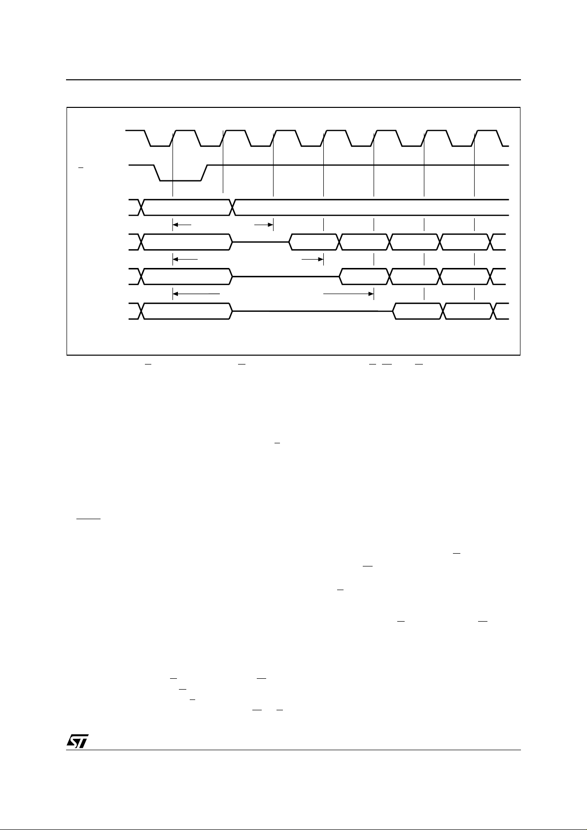
Figure 4. Single Synchronous Read Sequence (RSIG, RCFI, RSR instructions)
K
L
A20-A16
ADQ15-ADQ0
ADQ15-ADQ0
ADQ15-ADQ0
VALID ADDRESS
CONF. CODE 2
VALID ADDRESS VALID DATA NOT VALID
CONFIGURATION CODE 3
VALID ADDRESS VALID DATA
CONFIGURATION CODE 4
VALID ADDRESS NOT VALID
Both Chip Enable E and Output Enable G must be
at V
in order to read the output of the memory.
IL
Read array is the default state of the device when
exiting power down or after power up.
Burst Read. The device also supports a burst
read. In this mode a burst sequence is s tarted at
the first clock edge (risin g or falling according to
configuration settings) after th e falling edge of L
After a configurable delay of 2 to 5 clock cycles a
new data is output at each clock cycle. The burst
sequence may be configured for linear or interleaved order and for a length of 4, 8 words or for
continuous burst mode. Wrap and no-wrap modes
are also supported.
A WAIT
signal may be asserted to indicate to the
system that an output delay will occur. This delay
will depend on the starting address of the burst sequence; the worst case dela y will o ccur w hen the
sequence is crossing a 64 word boundary and the
starting address was at the end of a four word
boundary. See the Write Read Configuration Register (CR) Instruction for more details on all the
possible settings for the synchronous burst read
(see Table 14). It is possible to perform burst read
across bank boundary (all banks in read array
mode).
Write. Write operations are used to give I nstruction Commands to the memory or to latch Input
Data to be programmed. A write operation is initiated when Chip Enable E
at V
with Output Enable G at VIH. Addresses are
IL
latched on the rising edge of L
put Data are latched on the rising edge of W
and Write Enable W are
. Commands and In-
or E
whichever occurs first. Noise pulses of less than
5ns typical on E
NOT VALID
NOT VALID
VALID DATA
, W and G signals do not start a
NOT VALID
NOT VALID
write cycle. Write operations are asynchronous
and clock is ignored during write.
Dual Bank Operations. The Dual Bank allows to
run different operations simultaneously i n the tw o
banks. It is possible to read array data from one
bank while the other is programming, erasing or
reading any data (CFI, status register or electronic
.
signature).
Read and write cycles can be initiated for simulta-
neous operations in different banks without any
delay. Only one b ank at a time is all owed to be in
program or erase mode, while the other must be in
one of the read modes (see Table 8).
Commands must be writt en to an address within
the block targeted by that command.
Output Disa bl e . The data outputs are high impedance when the Output Enable G
Write Enable W
at VIH.
is at VIH with
Standby. The mem ory is in standby when C hip
Enable E
is at VIH and the P/E.C. is idle. The power consumption is reduced to the standby level
and the outputs are high impedance, independent
of the Output Enable G
or Write Enable W inputs.
Automatic Standby. When in Read mode, after
150ns of bus inactivity and when CMOS levels are
driving the addresses, the chip automatically enters a pseudo-standby mode where consumption
is reduced to the CMOS standby value, while outputs still drive the bus. The automatic standby feature is not available when the device is configured
for synchronous burst mode.
AI90022
9/52
Page 10
M58MR032C, M58MR032D
Table 9. Identifier Codes
Code Address (h) Data (h)
Manufacturer Code Bank Address + 00 0020
Device Code
Block Protection
Die Revision Code Bank Address + 03
Read Configuration Register Bank Address + 05
Lock Protection Register Bank Address + 80
Protection Register
Note: 1. DRC means Die Revisio n Co de.
CR means Read Configuration Register.
LPR means Lock Protection Register.
PR means Uni q ue Device Number and User Progra mmable OTP.
Reset/Power-down. The memory is in Powerdown when the Read Configuration Register is set
for Power-down and RP
sumption is reduced to the Power-down level, and
Outputs are in high impedance, independent of the
Chip Enable E
W
inputs. The memory is in reset when the Read
, Output Enabl e G or Write Enab le
Configuration Register is set for Reset and RP
at VIL
. The power consumption is the same of the
standby and the outputs are in hig h impedance.
After a Reset/Power down t he device defaults to
Top Bank Address + 01 88DA
Bottom Bank Address + 01 88DB
Protected and Unlocked
Unprotected and Unlocked 0000
Protected and Locked 0003
Unprotected and Locked 0002
Bank Address + 02
Bank Address + 81
Bank Address + 88
Block Locking. Any combination of blocks can
be temporarily protected against Program or
is at VIL. The power con-
Erase by setting the lock register and pulling WP
to VIL. The following summarizes the locking operation. All blocks are protected on power-up. They
can then be unprotected or protected with the Unprotect and Protect commands. The Lock com-
is
mand protects a b lock and prev ents it from being
unlocked when WP
overridden. Lock is cleared only when the dev ice
is reset or powered-down (see Protect instruction).
read array mode, the status register is set to 80h
and the read configuration register defaults to
asynchronous read.
0001
(1)
DRC
(1)
CR
(1)
LPR
(1)
PR
= 0. When WP = 1, Lock is
10/52
Page 11
M58MR032C, M58MR032D
INSTRUCTIONS AND COMMANDS
Eighteen instructions are available (see Tables 10
and 11) to perform Read Memory Array, Read Status Register, Read Electronic Signature, CFI Query, Block Erase, Bank Erase, Program, Tetra Word
Program, Double Word Program, Clear Status
Register, Program/Erase Suspend, Program/
Erase Resume, Block Protect, Block Unprotect,
Block Lock, Protection Register Program, Read
Configuration Register and Lock Protection Program.
Status Register ou tput may be read at any time,
during programming or erase, to monitor the
progress of the operation.
An internal Command Interface (C.I.) decodes the
instructions while an internal Program/Erase Controller (P/E.C.) handles all timing and verifies the
correct execution of the Program and Erase instructions. P/E.C. provides a Status Register
whose bits indicate operation and exit status of the
internal algorithms. The Command Interface is reset to Read Array when power is first applied,
when exiting from Reset or whenever V
than V
. Command sequence must be followed
LKO
is lowe r
DD
exactly. Any invalid combination of commands will
reset the device to Read Array.
Read (RD)
The Read instruction consists of o ne write cycle
(refer to Device Operations section) and places
the addressed bank in Read Array mode. When a
device reset occurs, the memo ry is in Read Array
as default. A read array command will be ignored
while a bank is programming or erasing. However
in the other bank a read array command will be accepted.
Read Status Register (RSR)
A bank’s Status Register indicates when a program or erase operation is complete and the success or failure of operation itself. Issue a Read
Status Register Instruction (70h) to read the Status Register content of t he addressed bank. The
status of the other bank is not affected by the command. The Read S tatus Register instruction may
be issued at any time, also when a Program/Erase
operation is ongoing. T he following Read operations output the content of the Status Register of
the addressed bank. The Status Register is
latched on th e fa lling edg e of E
can be read until E
must be toggled to update the latched data.
G
or G returns to VIH. Either E or
or G signals, and
Read Electronic Signature (RSIG)
The Read Electronic Signature instruction consists of one write cycle (refer to Device Operations
section) giving the com mand 90h to an address
Table 10. Commands
Hex Code Command
00h Invalid Reset
01h Protect Confirm
03h
10h Alterna tive Program Set-up
20h Block Erase Set-up
2Fh Lock Confirm
30h Double Word Program Set-up
40h Program Set-up
50h Clear Status Register
55h Tetra Word Program Set-up
60h
70h Read Status Register
80h Bank Erase Set-up
90h Read Electronic Signature
98h CFI Query
B0h Program/Erase Suspend
C0h
D0h
FFh Read Array
Write Read Configuration Register
Confirm
Protect Set-up and Write Read
Configuration Register
Protection Program and Lock Protection
Program
Program/Erase Resume, Erase Confirm
or Unprotect Confirm
within the bank A. A subsequent read in the ad-
dress of bank A will output the Manufacturer Code,
the Device Code, the protection Status of Blocks
of bank A, the Die Revision Code, the Protect ion
Register, or the Read Configuration Register (see
Table 9).
If the first write cycle of Read Electronic Signature
instruction is issued to an address within the bank
B, a subsequent read in an address of bank B will
output the protection Status of Blocks of bank B.
The status of the other bank is not affected by the
command (see Table 8).
See Tables 5, 6, 7 and 8 for the valid address. The
Electronic Signature can be read from the memory
allowing programming equipment or applications
to automatically match their interface to the char-
acteristics of M58MR032C and M58MR032D.
11/52
Page 12
M58MR032C, M58MR032D
Table 11. Instructions
Instruction Cyc. Ope ration
Read
RD
Memory
1+ Write BKA FFh
Array
RSR
Read Status
Register
1+ Write BKA 70h
Read
READ
RSIG
Electronic
1+ Write EA 90h
Signature
RCFI Read CFI 1+ Write CA 98h
CLRS
(5)
Register
1 Write BKA 50h
Clear Status
EE Block Erase 2 Write BA 20h Write BA D0h
BE Bank Erase 2 Write BKA 80h Write BKA D0h
PG Program 2 Write WA 40h or 10h Write WA WD
DPG
TPG
Double Word
Program
Tetra Word
Program
3 Write WA1 30h Write WA1 WD1
5 Write WA1 55h Write WA1 WD1
Address
(1,2)
Data
(3)
(1)
(1)
(1)
(1)
Address
(1,2)
Read
Address
BKA
EA ED
CA CD
Operation
Read
Read
Read
Read
Write WA2 WD2
Write WA2 WD2
(3)
Data
Data
Status
Register
Write WA3 WD3
PROGRAM/ERASE
Write WA4 WD4
Program
PES
Erase
1 Write BKA B0h
Suspend
Program
PER
Erase
1 Write BKA D0h
Resume
BP Block Protect 2 Write BA 60h Write BA 01h
Block
BU
Unprotect
PROTECT
BL Block Lock 2 Write BA 60h Write BA 2Fh
2 Write BA 60h Write BA D0h
Protection
PRP
Register
2 Write PA C0h Write PA PD
Program
Lock
LPRP
Protection
Register
2 Write LPA C0h Write LPA LPD
Program
CR
Write Read
Configuration
2 Write RCA 60h Write RCA 03h
CONFIGURATION
Register
12/52
Page 13

M58MR032C, M58MR032D
Note: 1. First cycle command address should be the same as the operation’s target address. The first cycle of the RD, RSR, RSIG or RCFI
CFI Query (RCFI)
The CFI Query Mode is associated to bank A. The
address of the first write cycle must be within the
bank A. The status of the other bank is not affected
by the command (see Table 8). Writing 98h the device enters the Common Flash Interface Query
mode. Next read operations in the bank A will read
the CFI data. Write a read instruction to return to
Read mode (refer to the Common Flash Interface
section).
Clear Status Register (CLSR)
The Clear Status Register uses a single write operation, which resets bits b1, b3, b4 e b5 of the status register. The Clear Status Register is executed
writing the command 50h independently of the applied V
the device returns to read array mode. The Clear
Status Register command clears only the status
register of the addressed bank.
Block Erase (EE)
Block erasure sets all the bits within the selected
block to ’1’. One block at a time can be erased. It
is not necessary to pre-program the block as the
P/E.C. will do it automatically before erasing. This
instruction use two writes cycles. The first command written is the Block Era se S et up c om m and
20h. The second command is the Erase Confirm
command D0h. An address within the block to be
erased should be given to the memory during t he
two cycles command. If the second command given is not an erase con firm, the status register bits
b4 and b5 are set and the instruction aborts.
instruction is followed by read operations in the bank array or special register. Any number of read cycles can occur after one command cycle.
2. BKA m eans Address within the bank;
BA means Block Address;
EA means Elec tronic Signature Address;
CA means C om m on Flash Interface Address;
WA means Wo rd Address;
PA means Pr otection Register Ad dress (see Ta bl e 7);
LPA means Loc k Protection Register Address (see Table 7);
RCA means Read Configuration Register Ad dress.
3. PD means Protect i on Data;
CD means Common Flash Interface Data;
ED means Electronic Si gnature Data;
WD means Data to be prog rammed at t he address loc a t i on WA;
LPD means Lock protection Register Da ta
4. WA1, WA2, WA3 and WA 4 m ust be consecutive add ress differi ng only for address bits A1- A0.
5. Read cycle after e CLSR instruction will output the memory array.
After writing the command, the device outputs status register data when any address within the bank
is read. At the end of the operation the bank will remain in read status register until a read array command is written.
Status Register bit b7 is ’0’ while the erasure is in
progress and ’1’ when it has completed. After completion the Status Register bit b5 returns ’1’ if there
has been an Erase Failure. Status register b it b1
returns ’1’ if the user is attempting t o e rase a protected block. Status Register bit b3 returns a ’1’ if
is below V
V
PP
V
. As data integrity cannot be guaranteed when
IL
. Erase aborts if RP turns to
PPLK
the erase operation is aborte d, the eras e m ust be
repeated (see Table 1 2). A Clear Status Register
voltage. After executing this comm and
PP
instruction must be issued t o reset b1, b3, b4 and
b5 of the Status Register. During the execution of
the erase by the P/E.C., the bank with the block in
erase accepts only the RS R (Read St atus Register) and PES (Program/Erase Suspend) instructions. See figure 19 for Erase Flowchart and
Pseudo Code.
Bank Erase (BE)
Bank erase sets all the bits within the selected
bank to ’1’. It is not necessary to pre-program the
block as the P/E.C. will do it automatically before
erasing.
This instruction uses two writes cycles. The first
command written is the Bank Erase set-up command 80h. The second command is the Erase
Confirm command D0h. An address within the
bank to be erased should be given to the memory
during the two cycles command. See the Block
Erase command section for status register bit details .
13/52
Page 14
M58MR032C, M58MR032D
Table 12. Status Register Bits
Mnemonic Bit Name
P/ECS 7 P/ECS
Status
ESS 6 Erase
Suspend
Status
Logic
Level
1 Ready Indicates the P/E.C. status, check during
0 Busy
1 Suspended
0
Definition Note
Program or Erase, and on completion before
checking bits b4 or b5 for Program or Erase
Success.
On an Erase Suspend instruction P/ECS and
In Progress or
Completed
ESS bits are set to ’1’. ESS bit remains ’1’ until
an Erase Resume instruction is given.
ES 5 Erase
PS 4 Program
VPPS 3 V
PSS 2 Program
BPS 1 Block
0 Reserved
Note: Logic level ’1’ is VIH and ’0’ is VIL.
Status
Status
Status
PP
Suspend
Status
Protection
Status
1 Erase Error ES bit is set to ’1’ if P/E.C. has applied the
0 Erase Success
1 Program Error
Program
0
Success
VPP Invalid,
1
Abort
V
0
1 Suspended
In Progress or
0
Completed
Program/Erase
1
on protected
Block, Abort
No operation to
0
protected blocks
Program (PG)
The Program instruction programs the array on a
word-by-word basis. The first command must be
given to the target block and only one partition can
be programmed at a time; the other partition must
be in one of the read m odes or in the erase sus pended mode (see Table 8).
This instruction uses two write cycles. The first
command written is the Program Set-up command
40h (or 10h). A second write operation latches the
Address and the Dat a to be writte n a nd starts the
P/E.C.
Read operations in the t argeted bank output the
Status Register content after the programming
has started.
The Status Register bit b7 returns ’ 0’ while the programming is in progress and ’1’ when it has completed. After completion the Status register bit b4
returns ’1’ if there has been a Program Failure (see
maximum number of erase pulses to the block
without achieving an erase verify.
PS bit set to ’1’ if the P/E.C. has failed to
program a word.
VPPS bit is set if the VPP voltage is below
V
when a Program or Erase instruction is
PPLK
PP
OK
executed. V
of the erase/program operation.
On a program Suspend instruction P/ECS and
PSS bits are set to ’1’. PSS remains ’1’ until a
Program Resume Instruction is given.
BPS bit is set to ’1’ if a Program or Erase
operation has been attempted on a protected
block.
is sampled only at the beginning
PP
Table 12). Status register bit b1 returns ’1’ if the
user is attempting to p rogram a protected block.
Status Register bit b3 returns a ’1’ if V
V
. Any attempt to write a ’1’ to an already pro-
PPLK
grammed bit will result in a program fail (status
register bit b4 set) if V
nored if V
PP
= V
PP1
PP
.
Programming aborts if RP
= V
goes to VIL. As data in-
and will be ig-
PPH
tegrity cannot be guaranteed when the program
operation is aborted, the block containing the
memory location must be erased and reprogrammed. A Clear Status Register instruction
must be issued to reset b5, b4, b3 and b1 of the
Status Register.
During the execution of the program by the P/E.C.,
the bank in prog ra mming accepts only the RSR
(Read Status Register) and PES (Program/Erase
Suspend) instructions. See Figure 16 for Program
Flowchart and Pseudo Code.
is below
PP
14/52
Page 15
Figure 5. Security Block Memory Map
Parameter Block # 0
88h
85h
84h
81h
80h
M58MR032C, M58MR032D
User Programmable OTP
Unique device number
Protection Register Lock 2 1 0
AI90023
Table 13. Protection States
(2)
Current State
(WP, DQ1, DQ0)
Program/Erase
Allowed
(1)
Next State After Event
(3)
Protect Unprotect Lo ck WP transition
100 Yes 10 1 100 111 000
101 No 101 100 111 001
110 Yes 11 1 110 111 011
111 No 111 110 111 011
000 Yes 00 1 000 011 100
001 No 001 000 011 101
011 No 011 011 011
Note: 1. All blo cks are protected at power-up, so the default configuration i s 001 or 101 acc ording to WP status.
2. Current state and Next st at e gives the protection status of a block. Th e protecti on status is def i ned by the wr ite protec t i n and by
DQ1 (= 1 for a locked block) and DQ0 (= 1 for a protected block) as read in the Read Electronic Signature instruction with A1 = V
and A0 = VIL.
3. Next state is the protection status of a block after a Protect or Unprotect or Lock command has been issued or after WP
its logic value.
4. A WP
transition to VIH on a locked block will restore the previous DQ0 value, giving a 111 or 110.
111 or 110
(4)
IH
has changed
15/52
Page 16

M58MR032C, M58MR032D
Doubl e Word Program (DP G)
This feature is offered to improve the programming
throughput, writing a page of two adjacent words
in parallel. The first command must be given to the
target block and only one partition can be programmed at a time ; the other p artition must be in
one of the read modes or in the erase suspended
mode (see Table 8).
The two words must differ only for the address A0.
Programming should not be attempted when V
is not at V
if V
is below V
PP
. The operation can also be executed
PPH
but result could be uncertain.
PPH
PP
These instructi on uses three write cycles. The first
command written is the Double Word Program
Set-Up command 30h. A second write operation
latches the Address and the Data of the first word
to be written, the third write operation latches the
Address and the Data of the second word to be
written and starts the P/E.C. (see Table 11).
Read operations in the t argeted bank output the
Status Register content after the programming
has started. The Status Register bit b7 ret urns ’0’
while the programming is in progress and ’1’ when
it has completed. After compl etion the S tatus register bit b4 returns ’1’ if there has been a Program
Failure. Status register bit b1 returns ’1’ if the user
is attempting to program a protected block. Status
Register bit b3 returns a ’1’ if V
is below V
PP
PPLK
Any attempt to write a ’1’ to an already programmed bit will result in a program fail (status
register bit b4 set). (See Table 12).
Programming aborts if RP
goes to VIL. As data integrity cannot be guaranteed when the program
operation is aborted, the memory location must be
erased and reprogrammed. A Clear Status Register instruction must be issued to reset b5, b4, b3
and b1 of the Status Register. During the execution of the program by the P/E.C., the bank in programming accepts only the RSR (Read Status
Register) instruction. See Figure 17 for Double
Word Program Flowchart and Pseudo code.
Tetra Word Program (TPG)
This feature is offered to improve the programming
throughput, writing a page of four adjacent words
in parallel. The first command must be given to the
target block and only one partition can be programmed at a time ; the other p artition must be in
one of the read modes or in the erase suspended
mode (see Table 8).
The four words must differ only for the addresses
A0 and A1. Programming should not be attempted
when V
is not at V
PP
be executed if V
PP
. The operation can also
PPH
is below V
but result could
PPH
be uncertain. These instruction uses five write cycles. The first comman d wri tten is t he Tetra Word
Program Set-Up command 55h. A second write
operation latches the Address and the Data of the
first word to be written, the third write operation
latches the Address an d the Data of the second
word to be written, the fourth write operation latches the Address and the Data of the third word to be
written, the fifth write operation latches the Address and the Data of the fourth word to be written
and starts the P/E.C. (see Table 11).
Read operations in the t argeted bank output the
Status Register content after the programming
has started. The Status Register bit b7 returns '0'
while the programming is in progress and '1' when
it has completed. After compl etion the S tatus register bit b4 returns '1' if there has been a Program
Failure. Status register bit b1 returns '1' if the user
is attempting to program a protected block. Status
Register bit b3 returns a '1' if V
is below V
PP
Any attempt to write a ’1’ to an already programmed bit will result in a program fail (status
register bit b4 set). (See Table 12).
Programming aborts if RP
goes to VIL. As data integrity cannot be guaranteed when the program
operation is aborted, the memory location must be
erased and reprogrammed. A Clear Status Register instruction must be issued to reset b5, b4, b3
and b1 of the Status Register. During the execution of the program by the P/E.C., the bank in programming accepts only the RSR (Read Status
Register) instruction. See Figure 17 for Tetra Word
Program Flowchart and Pseudo code.
.
Erase Suspend/Resume (PES/PER)
The Erase Suspend freezes , af t er a ce rtain latency period (within 25us), the erase operation and allows read in another block within the targeted bank
or program in the other block.
This instruction uses one write cycle B0h and the
address should be within the bank with the block
in erase (see Table 11). The device continues to
output status register data after the erase suspend
is issued. The status register bi t b7 and bi t b 6 are
set to ’1’ then the erase op eration has been sus pended. Bit b6 is set to '0' in case the erase is completed or in progress (see Table 12).
The valid commands while erase is suspended
are: Program/Erase Resume, Program, Read
Memory Array, Read St atus Regi ster, Read E lectronic Signature, CFI Query, Bloc k Protect, Block
Unprotect and Block Lock. The user can protect
the Block being erased issuing the B lock Protect
or Block Lock commands.
During a block erase suspend, the device goes
into standby mode by taking E
to VIH, which reduces active current draw. Erase is aborted if RP
to V
.
IL
If an Erase Suspend instruction was previously executed, the erase operation may be res umed by
issuing the command D0h using an address within
the suspended bank. The status register bit b6 and
bit b7 are cleared when erase resumes an d read
PPLK
turns
.
16/52
Page 17

M58MR032C, M58MR032D
operations output the status register after the
erase is resumed. Block erase cannot resume until
program operations initiated during block erase
suspend have completed. It is also possible to
nest suspends as follows: suspend erase in the
first partition, start programming in t he second or
in the same partition, suspend program ming and
then read from the second or the same pa rtition.
The suggested flowchart for erase suspend/resume features of the memory is shown from Figure 20.
Program Suspe nd /Re s ume ( PES/PER)
Program suspend is accepted only during the Program instruction execution. When a Program Suspend command is writt en to the C.I., the P/E.C.
freezes the Program operation.
Program Resume (PER) continues the Program
operation. Program Suspend (PES) consists of
writing the command B0h and the address should
be within the bank with the w ord in programming
(see Table 11).
The Status Register bit b2 is set to '1' (within 5µs)
when the program has been suspend ed. Bit b2 is
set to '0' in case the program is com pleted or in
progress (see Table 12).
The valid commands while program is suspen ded
are: Program/Erase Resume, Rea d Array, Read
Status Register, Read Electronic Signature, CFI
Query. During program suspend mode, the device
goes in standby mode by taking E
to VIH. This reduces active current consumption. Program is
aborted if RP
turns to VIL.
If a Program Suspend instruction was previously
executed, the Program operation may be resumed
by issuing the command D0h using an address
within the suspended bank (see Table 11). The
status register bit b2 and bit b7 are cleared when
program resumes and read operations out put the
status register after the erase is resumed (see Table 12). The suggested flowchart for program suspend/resume features of the memory is shown
from Figure 18.
Block Protect (BP)
The BP instruction use two write cycles. The f irst
command written is the protection set-up 60h. The
second command is block Protect comm and 01h,
written to an address within the block to be protected (see Table 11). If the sec ond command is not
recognized by the C.I the bit 4 and bit 5 of the status register will be set to indicate a wrong sequence of commands (see Table 12). To read the
status register write the RSR command.
Block Unprotect (BU)
The instr uction use t wo write cycl es. The fi rst c ommand written is the protection set-up 60h. The second command is block Unprotect command D0h,
written to an address within the block to be protected (see Table 11). If the sec ond command is not
recognized by the C.I the bit 4 and bit 5 of the status register will be set to indicate a wrong sequence of commands (see Table 12). To read the
status register write the RSR command.
Block Lock (BL)
The instr uction use t wo write cycl es. The fi rst c ommand written is the protection set-up 60h. The second command is block Lock command 2Fh,
written to an address within the block to be protected (see Table 11). If the second com mand is not
recognized by the C.I the bit 4 and bit 5 of the status register will be set to indicate a wrong sequence of commands. To read the status register
write the RSR command (see Table 12).
17/52
Page 18

M58MR032C, M58MR032D
BLOCK PROTECTION
The M58MR032C/M58MR032 D provide a flexible
protection of all the memory providing t he protection, un-protection and locking of any blocks. All
blocks are protected at power-up. Each block of
the array has two levels of protec t ion a gainst programming or erasing o peration. The first level is
set by the Block Protect instruction; a protected
block cannot be programmed or erased until a
Block Unprotect instruction is g iven for t hat bl oc k.
A second level of protection is set by the Block
Lock instruction, and requires the use of the WP
pin, according to the following scheme:
– when WP
is at VIH, the Lock status is overridden
and all blocks can be protected or unprotected;
– when WP
is at VIL, Lock status is enabled; the
locked blocks are protected, regardless of their
previous protect state, and protection status
cannot be changed. Bloc ks that are not locked
can still change their protection status;
– the lock status is cleared for all blocks at power
up.
The protection and lock status can be monitored
for each block using the Read Electronic Signature
(RSIG) instruction. Protected blocks will output a
'1' on DQ0 and locke d blocks will output a '1 ' in
DQ1 (see Table 13).
PROTECTION REGISTER PROGRAM (PRP)
and LO C K PROTEC TION REGISTE R
PROGRAM (LPRP)
The M58MR032C/M58MR032D features a 128-bit
protection register and a security Block in order t o
increase the prote ction of a system design. The
Protection Register is divided in two 64-bit segments. The first segm ent (81h to 84h) is a unique
device number, while the second one (85h to 88h)
can be program med by the user. When shipped
the user programmable segment is read at '1'. It
can be only programmed at '0'.
The user programmable segment c an be prot ected writing the bit 1 of the Protection Lock regi ster
(80h). The bit 1 protects al so the bi t 2 of the P rotection Lock Register.
The M58MR032C/M58MR032D feature a security
Block. The security Block is located at 1FF0001FFFFF (M58MR032C) or at 000000-000FFF
(M58MR032D) of the device. This block can be
permanently protected by the user programming
the bit 2 of the Protection Lock Register (see F igure 5).
The protection Register and the Protection Lock
Register can be read using the RSIG and RCFI instructions. A subsequent read in the address starting from 80h to 88h, the user will retrieve
respectively the Protection Lock register, the
unique device number segment and the OTP user
programmable register segment (see Table 23).
WRITE READ CONFIGURATION REGISTER
(CR).
This instruction uses two Coded Cycles, the first
write cycle is the write Read Configuration Register set-up 60h, the second write cycle is write
Read Configuration Register confirm 0 3h both to
Read Configuration Register address (see Table
11).
This instruction writes the contents of address bits
ADQ15-ADQ0 to bits CR15-CR0 of the Read Configuration Register (A20-A16 are don't care). At
Power-up the Read Configuration Regi ster is set
to asynchronous Read mode, Power-down disabled and bus invert (power save function) disabled. A description of the effects of each
configuration bit is given in Table 14.
Read mode (CR15). The device supports an
asynchronous page mode and a synchronous
burst mode. In asynchronous page mode, the default at power-up, data is internally read and stored
in a buffer of 4 words selected by ADQ0 and ADQ1
address inputs. In synchronous burst mode, the
device latches the starting address and t hen outputs a sequence of data that depends on the Read
Configuration Register settings (see Figures 10,
11 and 12).
Synchronous burst mode is supported in b oth parameter and main blocks; it is also possible to perform burst mode read across the banks.
Bus Invert configuration (CR14). This register
bit is used to enable the BINV pin functionality.
BINV functionality depends upon configuration
bits CR14 and CR15 (see Table 14 for configuration bits definition) as shown in Table 15. As output
pin BINV is active only when enabled (CR14 = 1)
in Read Array burst mode (CR15 = 0). As input pin
BINV is active only when enabled (CR14 = 1).
BINV is ignored when ADQ0-ADQ15 lines are
used as address inputs (addresses must not be inverted).
X-Latency (CR13-CR11). These configuration
bits define the number of clock cycles elapsing
going low to valid data available in b urst
from L
mode (see Figure 6). The correspondence between X-Latency set tings and the maximum sus tainable frequency mus t be calculated taking into
account some system parameters.
Two conditions must be satisfied:
–(n + 2) t
> t
–t
K
KQV
≥ t
K
ACC + tQVK_CPU
+ t
QVK_CPU
+ t
AVK_CPU
where "n" i s the chosen X-Lat ency configuration
code, t
is the clock period, t
K
AVK_CPU
is the address setup time guaranteed by the system CPU,
and t
QVK_CPU
is the data setup time required by
the system CPU.
18/52
Page 19

M58MR032C, M58MR032D
Table 14. Read Configuration Register (AS and Read CFI instructions)
Configuration Regis ter Function
Read mode
CR15
CR14
CR13-CR11
CR10
CR9 Reserved
CR8
CR7
CR6
CR5-CR4 Reserved
CR3
CR2-CR0
Note: 1. The R CR can be read v i a the RSIG com mand (90h). Bank A Address + 05h con tains the RCR data. See Tab l e 9.
2. All the bi ts in the RCR are set to default on device power-up or reset.
0 = Synchronous Burst mode read
1 = Asynchronous Page mode read (default)
Bus Invert configuration (power save)
0 = disabled (default)
1 = enabled
X-Latency
010 = 2 clock latency
011 = 3 clock latency
100 = 4 clock latency
101 = 5 clock latency
111 = reserved
Other configurations reserved
Power-down configuration
0 = power-down disabled (default)
1 = power-down enabled
Wait configuration
0 = WAIT
1 = WAIT
Burst order configuration
0 = Interleaved
1 = Linear (default)
Clock configuration
0 = Address latched and data output on the falling clock edge
1 = Address latched and data output on the rising clock edge (default)
Burst Wrap
0 = burst wrap within burst length set by CR2-CR0
1 = Don’t wrap accesses within burst length set by CR2-CR0 (default)
Burst length
001 = 4 word burst length
010 = 8 word burst length
111 = Continuous burst mode (requires CR7 = 1)
is active during wait state
is active one data cycle before wait state (default)
(1)
Table 15. BINV Configuration Bits
BINV
CR15 CR14
IN OUT
00X0
0 1 Active Active
10X0
1 1 Active 0
19/52
Page 20

M58MR032C, M58MR032D
Power-down configura tion (CR10). Th e RP pin
may be configured to give very low power consumption when driven low (pow er-down state). In
power-down the I
typical figure of I
(default at power-up) the RP
supply current is reduced to a
CC
; if this function is disabled
CC2
pin causes only a reset of the device and the supply current is the
stand-by value. The recovery time after a RP
pulse
is significantly longer when power-down is enabled (see Table 31).
Wait configuration (CR8). In burst mode WAIT
indicates whether the data on the output bus are
valid or a wait state must be inserted. The configuration bit determines if WAIT will be asserted one
clock cycle before the wait state or during the wait
state (see Figure 7). WAIT
is asserted during a
continuous burst and also during a 4 or 8 burst
length if no-wrap configuration is selected.
Burst order configuration (CR7) and Burst
Wrap configuration (CR3). See Table 16 for
burst order and length.
Figure 6. X-L at ency Configu ra tion Sequence
Clock configuration (CR6). In burst mode deter-
mines if address is latc hed and data is out put on
the rising or falling edge of the clock.
Burst length (CR2-CR0). In burst mode determines the number of words output by the memory.
It is possible to have 4 words, 8 words or a continuous burst mode, in which all the words are read
sequentially. In continuous burst mode the burst
sequence can cross the end of each of the two
banks (all banks in read array mode). In continuous burst mode or in 4, 8 words no-wrap it may
happen that the mem ory will stop the data ou tput
flow for a few clock cycles; this event is signaled by
going low until the output flow is resumed.
WAIT
The initial address dete rmines if the outpu t delay
will occur as w ell a s its du r ati o n. If the s tar t in g a ddress is aligned to a four words boundary no wait
states will be needed. If the starting address is
shifted by 1,2 or 3 positions from the four word
boundary, WAIT
will be asserted for 1, 2 or 3 clock
cycles when the burst sequence is crossing the
first 64 word boundary. WAIT
will be asserted only
once during a cont inuous burst access. S ee also
Table 16.
K
L
A20-A16
ADQ15-ADQ0
ADQ15-ADQ0
ADQ15-ADQ0
VALID ADDRESS
CONF. CODE 2
VALID ADDRESS VALID DATA VALID DATA
CONFIGURATION CODE 3
VALID ADDRESS VALID DATA
CONFIGURATION CODE 4
VALID ADDRESS VALID DATA
VALID DATA
VALID DATA
VALID DATA
VALID DATA
VALID DATA
AI90024
20/52
Page 21

Figure 7. Wai t Co nf i gu ra tio n Sequence
K
L
M58MR032C, M58MR032D
A20-A16
ADQ15-ADQ0
WAIT
CR8 = '0'
WAIT
CR8 = '1'
VALID ADDRESS
VALID ADDRESS
VALID DATA
VALID DATA NOT VALID VALID DATA
AI90025
21/52
Page 22

22/52
Table 16. Burst Order and Length Configuration
Starting
Mode
Address 4 Words 8 Words
Linear Interleaved Linear Interleaved
0 0-1-2-3 0-1-2-3 0-1-2-3-4-5-6-7 0-1-2-3-4-5-6-7 0-1-2-3-4-5-6...
1 1-2-3-0 1-0-3-2 1-2-3-4-5-6-7-0 1-0-3-2-5-4-7-6 1-2-3-4-5-6-7...
2 2-3-0-1 2-3-0-1 2-3-4-5-6-7-0-1 2-3-0-1-6-7-4-5 2-3-4-5-6-7-8...
3 3-0-1-2 3-2-1-0 3-4-5-6-7-0-1-2 3-2-1-0-7-6-5-4 3-4-5-6-7-8-9...
...
Wrap
7 7-4-5-6 7-6-5-4 7-0-1-2-3-4-5-6 7-6-5-4-3-2-1-0 7-8-9-10-11-12-13...
...
60 60-61-62-63-64-65-66...
61 61-62-63-WAIT-64-65-66...
62 62-63-WAIT-WAIT-64-65-66...
63 63-WAIT-WAIT-WAIT-64-65-66...
Linear Interleaved Linear Interleaved
0 0-1-2-3 0-1-2-3-4-5-6-7 0-1-2-3-4-5-6...
1 1-2-3-4 1-2-3-4-5-6-7-8 1-2-3-4-5-6-7...
M58MR032C, M58MR032D
Continuous Burst
2 2-3-4-5 2-3-4-5-6-7-8-9... 2-3-4-5-6-7-8...
3 3-4-5-6 3-4-5-6-7-8-9-10 3-4-5-6-7-8-9...
...
7 7-8-9-10 7-8-9-10-11-12-13-14 7-8-9-10-11-12-13...
No-wrap
...
60 60-61-62-63 60-61-62-63-64-65-66-67 60-61-62-63-64-65-66...
61 61-62-63-WAIT-64 61-62-63-WAIT-64-65-66-67-68 61-62-63-WAIT-64-65-66...
62 62-63-WAIT-WAIT-64-65 62-63-WAIT-WAIT-64-65-66-67-68-69 62-63-WAIT-WAIT-64-65-66...
63 63-WAIT-WAIT-WAIT-64-65-66 63-WAIT-WAIT-WAIT-64-65-66-67-68-69-70 63-WAIT-WAIT-WAIT-64-65-66...
Page 23

M58MR032C, M58MR032D
POWER CONSUMPTION
Power-down
The memory pro vides Reset/Power-down control
input RP
. The Power-down func tion can be activated only if the relevant Read Configuration Register bit is set to ’1’. In this case, when the RP
signal is pulled at VSS the supply current drops to
typically I
(see Table 26), the memory is dese-
CC2
lected and the outputs are in high impedance. If
is pulled to VSS during a Program or Erase op-
RP
eration, this operation is aborted and the memory
content is no longer valid (see Reset/Power-down
input description).
Power-up
The memory Command Interface is reset on Power-up to Read Array. Either E
V
during Power-up to allow maximum security
IH
or W must be tied to
and the possibility to write a command on the first
rising edge of W
. At Power-up the device is config-
ured as:
– Page mode: (CR15 = 1)
– Power-down disabled: (CR10 = 0)
– BINV disabled: (CR14 = 0).
All blocks are protecte d and unlocked.
, V
V
DD
and VPP are independent po wer sup-
DDQ
plies and can be biased in any order.
Supply Rails
Normal precautions must be taken for supply voltage decoupling; each device in a system should
have the V
itor close to the V
rails decoupled with a 0.1µF capac-
DD
DD
, V
and VSS pins. The PCB
DDQ
trace widths should be sufficient to carry the required V
program and erase currents.
DD
23/52
Page 24

M58MR032C, M58MR032D
COMMON FLASH INTERFACE (CFI)
The Comm on Fl ash In ter fac e (C FI) spec if i cati on i s
a JEDEC approved, standardized data structure
that can be read from the Flash memory device.
CFI allows a syste m software to query the flash
device to determine various electrical a nd timing
parameters, density information and functions
supported by the device. CFI allows the system to
easily interface to the Flash memory, to learn
about its features and parameters, enabling the
software to configure itself when necessary.
Tables 17, 18, 19, 20, 21, 22 and 23 show the address used to retrieve each data. The CFI data
structure gives information on the device, such as
the sectorization, the command set and some
electrical specifications. The CFI data structure
contains also a se curity area; in this section, a 64
bit unique security number is written, starting at
address 81h. This area can be accessed only in
read mode and there are no ways of changing the
code after it has been written by ST. Write a read
instruction to return to Read mode (see Table 11).
Refer to the CFI Query instruction to understand
how the M58MR032 enters the CFI Query mode.
Table 17. Query Structure Overvi ew
Offset Sub-section Name Description
00h Reserved Reserved for algorithm-specific information
10h CFI Query Identification String Command set ID and algorithm data offset
1Bh System Interface Information Device timing & voltage information
27h Device Geometry Definition Flash device layout
P Primary Algorithm-specific Extended Query table
A Alternate Algorithm-specific Extended Query table
80h Security Code Area
Note: T he Flash memor y display the CFI data structure when CFI Query comman d i s issued. In this table are listed the m ai n sub-se ctions
detailed in Ta bl es 18, 19, 20, 21, 22 and 23. Query data are al ways prese nted on the low est order data outputs.
Additional information specific to the Primary
Algorithm (optional)
Additional information specific to the Alternate
Algorithm (optional)
Lock Protection Register
Unique device Number and
User Programmable OTP
Table 18. CFI Query Identification String
Offset Sub-section Name Description Value
00h 0020h Manufacturer Code ST
01h
02h reserved Reserved
03h
04h-0Fh reserved Reserved
10h 0051h
11h 0052h "R"
12h 0059h "Y"
13h 0002h
14h 0000h
15h offset = P = 0039h
16h 0000h
17h 0000h Alternate Vendor Command Set and Control Interface ID Code
18h 0000h
19h value = A = 0000h
1Ah 0000h
Note: Query data are always present ed on the lowe st - order data outputs (AD Q0-ADQ7) only. ADQ8- A DQ15 are ‘0’.
1. DRC means Die Revision Code.
88DAh
88DBh
DRC
(1)
Device Code
Die Revision Code
Query Unique ASCII String "QRY"
Primary Algorithm Command Set and Control Interface ID code 16
bit ID code defining a specific algorithm
Address for Primary Algorithm extended Query table (see Table 20) p = 39h
second vendor - specified algorithm supported (note: 0000h means
none exists)
Address for Alternate Algorithm extended Query table
(0000h means none exists)
Top
Bottom
"Q"
NA
NA
24/52
Page 25

M58MR032C, M58MR032D
Table 19. CFI Query System Interface Information
Offset D ata Description Value
V
Logic Supply Minimum Program/Erase or Write voltage
1Bh 0017h
1Ch 0020h
1Dh 0017h
1Eh 00C0h
1Fh 0004h
20h 0004h
21h 000Ah
22h 0000h
23h 0004h
24h 0004h
25h 0 004h
26h 0000h
DD
bit 7 to 4 BCD value in volts
bit 3 to 0 BCD value in 100 millivolts
Logic Supply Maximum Program/Erase or Write voltage
V
DD
bit 7 to 4 BCD value in volts
bit 3 to 0 BCD value in 100 millivolts
V
[Programming] Supply Minimum Program/Erase voltage
PP
bit 7 to 4 HEX value in volts
bit 3 to 0 BCD value in 100 millivolts
[Programming] Supply Maximum Program/Erase voltage
V
PP
bit 7 to 4 HEX value in volts
bit 3 to 0 BCD value in 100 millivolts
n
µs
n
n
µs
ms
n
times typical
Typical timeout per single byte/word program = 2
Typical timeout for tetra word program = 2
Typical timeout per individual block erase = 2
Typical timeout for full chip erase = 2
Maximum timeout for word program = 2
Maximum timeout for tetra word = 2
n
ms
n
times typical
n
times typical
Maximum timeout per individual block erase = 2
Maximum timeout for chip erase = 2
n
times typical
1.7V
2V
1.7V
12V
16µs
16µs
1s
NA
512µs
512µs
16s
NA
25/52
Page 26

M58MR032C, M58MR032D
Table 20. Device Geometry Definition
Offset Word
Mode
27h 0016h
28h
29h
2Ah
2Bh
2Ch 0003h Number of Erase Block Regions within the device
2Dh
2Eh
2Fh
30h
31h
32h
33h
34h
M58MR032C
35h
36h
37h
38h
2Dh
2Eh
2Fh
30h
31h
32h
33h
34h
M58MR032D
35h
36h
37h
38h
Data Description V alue
n
in number of bytes
0001h
0000h
0003h
0000h
002Fh
0000h
0000h
0001h
000Eh
0000h
0000h
0001h
0007h
0000h
0020h
0000h
0007h
0000h
0020h
0000h
000Eh
0000h
0000h
0001h
002Fh
0000h
0000h
0001h
Device Size = 2
Flash Device Interface Code description
Maximum number of bytes in multi-byte program or page = 2
bit 7 to 0 = x = number of Erase Block Regions
It specifies the number of regions within the device containing one or more
contiguous Erase Blocks of the same size.
Region 1 Information (main block - Bank B)
Number of identical-size erase block = 002Fh+1
Region 1 Information (main block - Bank B)
Block size in Region 1 = 0100h * 256 byte
Region 2 Information (main block - Bank A)
Number of identical-size erase block = 000Eh+1
Region 2 Information (main block - Bank A)
Block size in Region 2 = 0100h * 256 byte
Region 3 Information (parameter block - Bank A)
Number of identical-size erase block = 0007h+1
Region 3 Information (parameter block - Bank A)
Block size in Region 3 = 0020h * 256 byte
Region 1 Information (parameter block - Bank A)
Number of identical-size erase block = 0007h+1
Region 1 Information (parameter block - Bank A)
Block size in Region 1 = 0020h * 256 byte
Region 2 Information (main block - Bank A)
Number of identical-size erase block = 000Eh+1
Region 2 Information (main block - Bank A)
Block size in Region 2 = 0001h * 256 byte
Region 3 Information (parameter block - Bank B)
Number of identical-size erase block = 002Fh+1
Region 3 Information (parameter block - Bank B)
Block size in Region 3 = 0001h * 256 byte
4 MByte
x16
Async.
n
8 Byte
3
48
64 KByte
15
64 KByte
8
8 KByte
8
8 KByte
15
64 KByte
48
64 KByte
26/52
Page 27

M58MR032C, M58MR032D
Table 21. Primary Algorithm-Specific Extended Qu ery Ta bl e
Offset
(P)h = 39h 0050h
(P+3)h = 3Ch 0031h Major version number, ASCII "1"
(P+4)h = 3Dh 0030h Minor version number, ASCII "0"
Data Descript ion Value
0052h "R"
0049h "I"
Primary Algorithm extended Query table unique ASCII string “PRI”
"P"
(P+5)h = 3Eh 00E6h Extended Query table contents for Primary Algorithm. Address (P+5)h
0003h
(P+7)h 0000h
(P+8)h 0000h
(P+9)h = 42h 0001h Supported Functions after Suspend
(P+A)h = 43h 0003h Block Protect Status
(P+B)h 0000h
(P+C)h = 45h 0018h V
contains less significant byte.
bit 0 Chip Erase supported (1 = Yes, 0 = No)
bit 1 Erase Suspend supported (1 = Yes, 0 = No)
bit 2 Program Suspend supported (1 = Yes, 0 = No)
bit 3 Legacy Lock/Unlock supported (1 = Yes, 0 = No)
bit 4 Queued Erase supported (1 = Yes, 0 = No)
bit 5 Instant individual block locking supported (1 = Yes, 0 = No)
bit 6 Protection bits supported (1 = Yes, 0 = No)
bit 7 Page mode read supported (1 = Yes, 0 = No)
bit 8 Synchronous read supported (1 = Yes, 0 = No)
bit 9 Simultaneous operation supported (1 = Yes, 0 = No)
bit 10 to 31 Reserved; undefined bits are ‘0’. If bit 31 is ’1’ then another 31
bit field of optional features follows at the end of the bit-30
field.
Read Array, Read Status Register and CFI Query
bit 0 Program supported after Erase Suspend (1 = Yes, 0 = No)
bit 7 to 1 Reserved; undefined bits are ‘0’
Defines which bits in the Block Status Register section of the Query are
implemented.
bit 0 Block protect Status Register Protect/Unprotect
bit active (1 = Yes, 0 = No)
bit 1 Block Lock Status Register Lock-Down bit active (1 = Yes, 0 = No)
bit 15 to 2 Reserved for future use; undefined bits are ‘0’
Logic Supply Optimum Program/Erase voltage (highest performance)
DD
No
Yes
Yes
No
No
Yes
Yes
Yes
Yes
Yes
Yes
Yes
Yes
1.8V
(P+D)h = 46h 00C0h V
(P+E)h = 47h
(P+F)h
(P+10)h
(P+11)h
(P+12)h
0000h Reserved
bit 7 to 4 HEX value in volts
bit 3 to 0 BCD value in 100 mV
Supply Optimum Program/Erase voltage
PP
bit 7 to 4 HEX value in volts
bit 3 to 0 BCD value in 100 mV
12V
27/52
Page 28

M58MR032C, M58MR032D
Table 22. Burst Read Information
Offset
(P)+13h = 48h 0003h Page-mode read capability
Data Description Value
bits 0-7 ’n’ such that 2
page bytes. See offset 28h for device word width to
determine page-mode data output width. 00h indicates
no read page buffer.
n
HEX value represents the number of read-
8 Byte
(P+14)h = 49h 0003h Number of synchronous mode read configuration fields that follow. 00h
indicates no burst capability.
(P+15)h = 4Ah 0001h Synchronous mode read capability configuration 1
bit 3-7 Reserved
bit 0-2 ’n’ such that 2
number of continuous synchronous reads when the device is
configured for its maximum word width. A value of 07h
indicates that the device is capable of continuous linear bursts
that will output data until the internal burst counter reaches
the end of the device’s burstable address space. This field’s
3-bit value can be written directly to the read configuration
register bit 0-2 if the device is configured for its maximum
word width. See offset 28h for word width to determine the
burst data output width.
(P+16)h = 4Bh 0002h Synchronous mode read capability configuration 2 8
(P+17)h = 4Ch 0007h Synchronous mode read capability configuration 3 Cont.
(P+18)h = 4Dh 0028h Max operating clock frequency (MHz) 40 MHz
(P+19)h = 4Eh 0001h Supported handshaking signal (WAIT
bit 0 during synchronous read (1 = Yes, 0 = No)
bit 1 during asynchronous read (1 = Yes, 0 = No)
n+1
HEX value represents the maximum
pin)
Yes
No
Table 23. Security Code Area
Offset Data Description
80h 0000-0000-0000-0XX0 Lock Protection Register
81h XXXX
82h XXXX
83h XXXX
84h XXXX
85h XXXX
86h XXXX
87h XXXX
88h XXXX
64 bits: unique device number
64 bits: User Programmable OTP
3
4
28/52
Page 29

M58MR032C, M58MR032D
Table 24. AC Measuremen t Cond itions
Input Rise and Fall Times
Input Pulse Voltages
Input and Output Timing Ref. Voltages
0 to V
V
≤
DDQ
4ns
DDQ
/2
Figure 9. AC Testing Load Circuit
V
/ 2
DDQ
1N914
3.3kΩ
Figure 8. Tes ting Inp ut/ Output Wav ef orms
DEVICE
UNDER
V
DDQ
V
/2
DDQ
0V
AI90026
Table 25. Capacitance
(T
= 25 °C, f = 1 MHz)
A
(1)
Symbol Parameter Test Condition Min Max Unit
V
V
IN
OUT
= 0V
= 0V
C
IN
C
OUT
Note: 1. Sampled only, not 100% tested.
Input Capacitance
Output Capacitance
TEST
CL = 30pF
CL includes JIG capacitance
6pF
12 pF
OUT
AI90027
29/52
Page 30

M58MR032C, M58MR032D
Table 26. DC Characteristics
(T
= –40 to 85°C; VDD = V
A
Symbol Parameter Test Condition Min Typ Max Unit
= 1.7V to 2.0V)
DDQ
I
Input Leakage Current
LI
I
Output Leakage Current
LO
Supply Current
(Asynchronous Read Mode)
I
CC1
Supply Current
(Synchronous R ead Mode
Continuous Burst)
I
CC2
I
CC3
I
CC4
I
CC5
I
PP1
I
PP2
V
V
V
V
V
V
V
PPLK
Note: 1. Sampled only, not 100% tested.
Supply Current
(Power-down)
Supply Current (Standby)
Supply Current
(1)
(Program or Erase)
Supply Current
(1)
(Dual Bank)
VPP Supply Current (Program
or Erase)
VPP Supply Current (Standby
or Read)
Input Low Voltage –0.5 0.4 V
IL
Input High Voltage
IH
Output Low Voltage
OL
Output High Voltage CMOS
OH
VPP Supply Voltage
PP1
VPP Supply Voltage
PPH
Program or Erase Lockout 1 V
2. V
may be conne ct ed to 12V pow er supply for a total of less than 100 hrs.
PP
0V ≤ V
0V ≤ V
= VIL, G = VIH, f = 6MHz
E
= VIL, G = VIH, f = 40MHz
E
RP
E
Word Program, Block Erase
≤ V
IN
DDQ
≤ V
OUT
DDQ
= VSS ± 0.2V
= VDD ± 0.2V
in progress
±1 µA
±5 µA
10 20 mA
20 30 mA
210µA
15 50 µA
10 20 mA
Program/Erase in progress
in one Bank, Asynchronous
20 40 mA
Read in the other Bank
Program/Erase in progress
in one Bank, Synchronous
30 50 mA
Read in the other Bank
V
= 12V ± 0.6V
PP
V
≤ V
PP
CC
V
= 12V ± 0.6V
PP
I
= 100µA
OL
I
= –100µA V
OH
Program, Erase
V
–0.4 V
DDQ
–0.1
DDQ
V
–0.4 V
DDQ
510mA
0.2 5 µA
100 400 µA
+ 0.4
DDQ
0.1 V
+ 0.4
DDQ
Double/Tetra Word Program 11.4 12.6 V
V
V
V
30/52
Page 31

Table 27. Asynchronous Read AC Characteristics
(T
= –40 to 85°C; VDD = V
A
= 1.7V to 2.0V)
DDQ
M58MR032C, M58MR032D
M58MR032
Symbol Alt Parameter Test Condition
t
AVAV
t
AVLH
t
AVQV
t
AVQV1
t
EHQX
(1)
t
EHQZ
t
ELLH
(2)
t
ELQV
(1)
t
ELQX
t
GHQX
(1)
t
GHQZ
(2)
t
GLQV
(1)
t
GLQX
t
LHAX
t
LHGL
t
LLLH
t
LLQV
t
LLQV1
Note: 1. Sampled only, not 100% tested.
may be delayed by up to t
2. G
t
RC
t
AVAVDH
t
ACC
t
PAGE
t
OH
t
HZ
t
ELAVDH
t
CE
t
LZ
t
OH
t
DF
t
OE
t
OLZ
t
AVDHAX
t
AVDLAVDH
t
AVDLQV
Address Valid to Next
Address Valid
Address valid to Latch
Enable High
Address Valid to Output
Valid (Random)
Address Valid to Output
Valid (Page)
Chip Enable High to Output
T ransition
Chip Enable High to Output
Hi-Z
Chip Enable Low to Latch
Enable High
Chip Enable Low to Output
Valid
Chip Enable Low to Output
Transition
Output Enable High to
Output Transition
Output Enable High to
Output Hi-Z
Output Enable Low to
Output Valid
Output Enable Low to
Output Transition
Latch Enable High to
Address Transition
Latch Enable High to
Output Enable Low
Latch Enable Pulse Width
Latch Enable Low to
Output Valid (Random)
Latch Enable Low to
Output Valid (Page)
- t
ELQV
after the fal ling edge of E without increasi ng t
GLQV
= VIL, G = V
E
= V
G
= VIL, G = V
E
= VIL, G = V
E
= V
G
= V
G
= VIL, G = V
E
= V
G
= V
G
= V
E
= V
E
= V
E
= V
E
= VIL, G = V
E
= V
E
E
= VIL, G = V
= V
E
= V
E
Unit100 120
Min Max Min Max
100 120 ns
IL
IH
IL
IL
IH
IL
IL
IL
IL
IL
IL
IH
IL
IH
IL
IL
10 10 ns
IL
IL
100 120 ns
45 45 ns
00ns
20 20 ns
10 10 ns
100 120 ns
00ns
00ns
20 20 ns
25 35 ns
00ns
10 10 ns
10 10 ns
10 10 ns
100 120 ns
45 45 ns
.
ELQV
31/52
Page 32

M58MR032C, M58MR032D
Figure 10. Asynchronous Read AC Wavefor ms
VALID ADDRESS
VALID DATA VALID ADDRESS
tEHQZ
AI90028
tGHQZ
tGHQX
tEHQX
tAVAV
VALID ADDRESS
ADQ0-ADQ15
tAVQV
VALID ADDRESS
A16-A20
tAVLH tLHAX
tGLQV
tGLQX
tLLQV
tLLLH
L
tELLH
tELQV
tELQX
tLHGL
E
G
Note: Write Enable (W) = High.
32/52
Page 33

Figure 11. Page Read AC Waveforms
M58MR032C, M58MR032D
AI90029
tAVQV1
VALID ADDRESS VALID DATA VALID ADDRESSVALID DATA VALID DATA VALID ADDRESS VALID DATA
tAVLH tLHAX
VALID ADDRESS
VALID ADDRESS
tLLQV1
tLLQV
tGHQZ
tGLQV
tLHGL
tELQV
ADQ0-ADQ15
A16-A20
L
E
G
33/52
Page 34

M58MR032C, M58MR032D
Table 28. Synchronous Burst Read AC Characteristics
(T
= –40 to 85°C; VDD = V
A
Symbol Alt Parameter Test Condition
t
AVK
t
ELK
t
t
KAX
t
KHKL
t
KLKH
K
t
AVCLKH
t
CELCLKH
t
CLK
t
CLKHAX
t
CLKHCLKL
t
CLKLCLKH
Address Valid to Clock 7 7 ns
Chip Enable Low to Clock 7 7 ns
Clock Period 25 25 ns
Clock to Address Transition
Clock High 5 5 ns
Clock Low 5 5 ns
Clock to Data Valid
t
KQV
t
CLKHQV
Clock to BINV Valid
Clock to WAIT Valid
Clock to Output Transition
t
KQX
t
CLKHQX
Clock to BINV Transition
Clock to WAIT Transition
t
LHAX
t
LLK
t
ADVHAX
t
AVDLCLKH
Latch Enable High to
Address Transition
Latch Enable Low to Clock 7 7 ns
= 1.7V to 2.0V)
DDQ
E
= VIL, G = V
E
= VIL, G = V
E
= V
M58MR032
Unit100 120
Min Max Min Max
IH
IL
13 13 ns
IL
20 20 ns
44ns
13 13 ns
34/52
Page 35

Figure 12. Synchronous Burst Read
M58MR032C, M58MR032D
AI90030
VALID
VALID DATA
VALID
tEHQX
tKQXtKQV
tEHQZ
VALID
tGHQZ
tGHQX
tKQV tKQV
VALID
tKQX
tK
VALID
tKQX
note 2 note 3
VALID ADDRESS VALID
ADQ0-ADQ15
tLLLH
tAVLH
VALID ADDRESS
A16-A20
L
tLLK
tAVK
note 1
K
tELK tKAX
tGLQX
signal can be c onfigured to be active du ri ng wait state or one cycle be l ow wait state.
signal is asserted only when burst l ength is configured as continuous (see Burst Read section for further informa tion).
3. WAIT
2. WAIT
E
G
BINV
WAIT
Note: 1. The num ber of clock cy cles to be inserted depe nds upon the x-l atency set in th e read configuration register.
35/52
Page 36

M58MR032C, M58MR032D
Table 29. Write AC Characteristics, Write Enable Controlled
(T
= –40 to 85 °C; VDD = V
A
= 1.7V to 2.0V)
DDQ
M58MR032
Symbol Alt Parameter
t
AVAV
t
AVLH
t
DVWH
t
ELLH
t
ELWL
t
GHLL
t
GHWL
t
LHAX
t
LHWH
t
LLLH
t
VDHEL
t
VPPHWH
t
WHDX
t
WHEH
t
WHGL
t
WHLL
t
WHVPPL
t
WHWL
t
WHWPV
t
WLWH
t
WPVWH
t
Address Valid to Next Address Valid 100 120 ns
WC
Address Valid to Latch Enable High 10 10 ns
t
Input Valid to Write Enable High 40 40 ns
DS
Chip Enable Low to Latch Enable High 10 10 ns
t
Chip Enable Low to Write Enable Low 0 0 ns
CS
Output Enable High to Latch Enable Low 20 20 ns
Output Enable High to Write Enable Low 20 20 ns
Latch Enable High to Address Transition 10 10 ns
Latch Enable High to Write Enable High 10 10 ns
Latch Enable Pulse Width 10 10 ns
t
VCSVDD
VPP High to Write Enable High
t
Write Enable High to Input Transition 0 0 ns
DH
t
Write Enable High to Chip Enable High 0 0 ns
CH
t
Write Enable High to Output Enable Low 0 0 ns
OEH
Write Enable High to Latch Enable Low 0 0 ns
Write Enable High to VPP Low
t
Write Enable High to Write Enable Low 30 30 ns
WPH
Write Enable High to Write Protect Valid 200 200 ns
t
Write Enable Low to Write Enable High 50 50 ns
WP
Write Protect Valid to Write Enable High 200 200 ns
High to Chip Enable Low
Unit100 120
Min Max Min Max
50 50 µs
200 200 ns
200 200 ns
36/52
Page 37

Figure 13. Write AC Waveforms, W Controlled
tWHLL
M58MR032C, M58MR032D
AI90031
tWHGL
tWHVPPL
VALID
DATA VALIDADDRESS VALID
tAVAV
tDVWH tWHDX
tLHAX
ADDRESS VALID
tAVLH
tLHWH
tLLLH
tWLWH
tELLH
tELWL
tGHLL
tWPVWH tWHWPV
tGHWL
tVPPHWH
PPH
V
tVDHEL
PP1
V
ADQ0-ADQ15
A16-A20
BINV VALID
L
W
E
G
WP
PP
V
V
DD
37/52
Page 38

M58MR032C, M58MR032D
Table 30. Write AC Characteristics, Chip Enable Controlled
(T
= –40 to 85 °C; VDD = V
A
= 1.7V to 2.0V)
DDQ
M58MR032
Symbol Alt Parameter
t
AVAV
t
AVLH
t
DVEH
t
EHDX
t
EHEL
t
EHWH
t
ELEH
t
ELLH
t
GHLL
t
LHAX
t
LHEH
t
LLLH
t
VDHEL
t
VPPHEH
t
EHVPPL
t
EHWPV
t
WLEL
t
WPVEH
t
Address Valid to Next Address Valid 100 120 ns
WC
Address Valid to Latch Enable High 10 10 ns
t
Input Valid to Chip Enable High 40 40 ns
DS
t
Chip Enable High to Input Transition 0 0 ns
DH
t
Chip Enable High to Chip Enable Low 30 30 ns
CPH
t
Chip Enable High to Write Enable High 0 0 ns
WH
t
Chip Enable Low to Chip Enable High 60 60 ns
CP
Chip Enable Low to Latch Enable High 10 10 ns
Output Enable High to Latch Enable Low 20 20 ns
Latch Enable High to Address Transition 10 10 ns
Latch Enable High to Chip Enable High 10 10 ns
Latch Enable Pulse Width 10 10 ns
t
VCSVDD
VPP High to Chip Enable High
Chip Enable High to VPP Low
Chip Enable High to Write Protect Valid 200 200 ns
t
Chip Enable Low to Chip Enable Low 0 0 ns
WS
Write Protect Valid to Chip Enable High 200 200 ns
High to Chip Enable Low
Unit100 120
Min Max Min Max
50 50 µs
200 200 ns
200 200 ns
38/52
Page 39

Figure 14. Write AC Waveforms, E Controlled
M58MR032C, M58MR032D
AI90032
DATA VALIDADDRESS VALID
tDVEH tEHDX
tLHAX
ADDRESS VALID
tAVLH
VALID
tLHEH
tLLLH
tEHWH
tELLH
tEHEL
tELEH
VALID
tWPVEH tEHWPV
tEHVPPL
tVPPHEH
PPH
V
PP1
V
ADQ0-ADQ15
A16-A20
BINV
tGHLL
tWLEL
L
W
E
G
WP
tVDHEL
PP
V
V
DD
39/52
Page 40

M58MR032C, M58MR032D
Figure 15. Reset and Power-up AC Waveforms
W,
E, G
L,
RP
tPHWL
tPHEL
tPHGL
tPHWL
tPHEL
tPHGL
VDD, V
tVDHPH
DDQ
Power-up
tPLPH
AI90033
Table 31. Reset and Power-up AC Characteristics
Symbol Parameter Test Condition Min Unit
(1,2)
t
PLPH
t
PHEL
t
PHLL
t
PHWL
t
VDHPH
Note: 1. The de vi ce Reset is p ossible but not guarant eed if t
2. Sampled only, not 100% tested.
3. It is im portant to ass ert RP
RP Pulse Width 100 ns
During Program and Erase 50 µs
Reset High to Device Enabled
Other Conditions 30 ns
(3)
Supply Valid to Reset High 50 µs
< 100ns.
PLPH
in order to all ow proper CP U i ni tializat i on during Po wer-up or Sy st em reset.
Table 32. Program, Erase Times and Program , Erase End urance Cycl es
(T
= –40 to 85°C; VDD = V
A
Parameter Min
Parameter Block (4 K-Word) Erase (Preprogrammed) 2.5 0.5 1 sec
= 1.7V to 2.0V, VPP = VDD unless otherwise specified)
DDQ
Max
(1)
Typ
Typical after
100k W/E Cycles
Unit
Main Block (32 K-Word) Erase (Preprogrammed) 10 1 3 sec
Bank Erase (Preprogrammed, Bank A) 4 sec
Bank Erase (Preprogrammed, Bank B) 15 sec
Chip Program
(2)
Chip Program (DPG, V
Word Program
(3)
= 12V)
PP
(2)
200 10 10 µs
40 sec
20 sec
Double Word Program 200 10 10 µs
Tetra Word Program 200 10 10 µs
Program/Erase Cycles (per Block) 100,000 cycles
Note: 1. Max values refer t o the maximum t i me allow ed by the internal algorithm before error bi t is set. Worst case condi tions program or
erase shou l d perform significantl y better.
2. Exc l udes the time needed to exe cute the sequence for program instruction.
3. Sam e tim i ng value if V
= 12V.
PP
40/52
Page 41

M58MR032C, M58MR032D
Figure 16. Program Flow c hart and Pseudo Code
Start
Write 40h or 10h
Command
Write Address
& Data
Read Status
Register
b7 = 1
YES
b3 = 0
YES
NO
NO
NO
Suspend
YES
Suspend
Loop
VPP Invalid
Error (1, 2)
(1)
Program instruction:
– write 40h or 10h command
– write Address & Data
(memory enters read status state after
the Program instruction)
do:
– read status register (E or G must be
toggled) if PES instruction given execute
suspend program loop
while b7 = 1
If b3 = 1, VPP invalid error:
– error handler
b4 = 0
b1 = 0
End
Note: 1. Status check of b1 (Protected Blo ck), b3 (VPP Invalid) and b4 (P rogram Error) can be made af t er each program ope ration or after
a program sequence.
2. If an er ror is found, the Status Register m ust be cleared (CLRS instruction) before fu rther P/E. C. operation s.
NO
YES
NO
YES
Program
Error (1, 2)
Program to Protected
Block Error (1, 2)
If b4 = 1, Program error:
– error handler
If b1 = 1, Program to protected block error:
– error handler
AI90034
41/52
Page 42

M58MR032C, M58MR032D
Figure 17. Double Wo rd Progr am and Tet ra Word Program Flowc hart and Pseudo code
Start
Write 55h
Command
Write Address 1
& Data 1
Write Address 2
& Data 2
Write Address 3
& Data 3
Write Address 4
& Data 4
Read Status
Register
NO
Suspend
YES
DPG instruction:
– write 30h command
– write Address 1 & Data 1 (3)
– write Address 2 & Data 2 (3)
(memory enters read status state after
the Program instruction)
TPG instruction:
– write 55h command
– write Address 1 & Data 1 (4)
– write Address 2 & Data 2 (4)
– write Address 3 & Data 3 (4)
– write Address 4 & Data 4 (4)
(memory enters read status state after
the Program instruction)
do:
– read status register (E or G must be
toggled) if PES instruction given execute
suspend program loop
(1)
while b7 = 1
If b3 = 1, VPP invalid error:
– error handler
If b4 = 1, Program error:
– error handler
If b1 = 1, Program to protected block error:
– error handler
AI90035
YES
YES
YES
YES
NO
NO
NO
NO
Program to Protected
Block Error (1, 2)
b7 = 1
b3 = 0
b4 = 0
b1 = 0
End
Note: 1. Status check of b1 (Protected Block), b3 (VPP Invalid ) and b4 (Program Er ror) can be made after each program operation or after
a program sequence.
2. If an er ror is found, the Status Register m ust be cleared (CLRS instruction) before fu rther P/E. C. operation s.
3. Address 1 and add ress 2 must be consecutive addresses di ffering only for address bit A0.
4. Address, ad dress 2, address 3 and ad dress 4 must be co nsecutive add resses diff er i ng only for addr ess bit A1-A0.
Suspend
Loop
VPP Invalid
Error (1, 2)
Program
Error (1, 2)
42/52
Page 43

Figure 18. Program Suspend & Resume Flowchart and Pseudo Code
Start
Write B0h
Command
M58MR032C, M58MR032D
Write 70h
Command
Read Status
Register
b7 = 1
YES
b2 = 1
YES
Write a read
Command
Read data from
another address
Write D0h
Command
Program Continues
NO
NO
Program Complete
Write FFh
Command
Read Data
PES instruction:
– write B0h command
do:
– read status register
(E or G must be toggled)
while b7 = 1
If b2 = 0 Program completed
PER instruction:
– write D0h command to resume
the program
– if the program operation completed
then this is not necessary.
The device returns to Read Array as
normal (as if the Program/Erase
suspend was not issued).
AI90036
43/52
Page 44

M58MR032C, M58MR032D
Figure 19. Block Erase Flowchart and Pseudo Code
Start
Write 20h
Command
Write Block Address
& D0h Command
Read Status
Register
b7 = 1
b3 = 0
b4, b5 = 0
b5 = 0 Erase Error (1)
NO
YES
NO
YES
NO
YES
NO
Suspend
Sequence Error (1)
NO
VPP Invalid
Error (1)
Command
EE instruction:
– write 20h command
– write Block Address (A12-A20) &
command D0h
(memory enters read status state after
the EE instruction)
do:
– read status register (E or G must be
toggled) if PES instruction given execute
suspend erase loop
YES
Suspend
Loop
while b7 = 1
If b3 = 1, VPP invalid error:
– error handler
If b4, b5 = 1, Command sequence error:
– error handler
If b5 = 1, Erase error:
– error handler
44/52
b1 = 0
End
YES
YES
NO
Erase to Protected
Block Error (1)
If b1 = 1, Erase to protected block error:
– error handler
AI90037
Page 45

Figure 20. Erase Suspend & Resume Flowchart and Pseudo Code
Start
Write B0h
Command
M58MR032C, M58MR032D
Write 70h
Command
Read Status
Register
b7 = 1
b6 = 1
Read data from
another block
or
Program/Protection Program
or
Block Protect/Unprotect/Lock
Write D0h
Command
Erase Continues
NO
YES
NO
YES
Erase Complete
Write FFh
Command
Read Data
PES instruction:
– write B0h command
do:
– read status register
(E or G must be toggled)
while b7 = 1
If b6 = 0, Erase completed
PER instruction:
– write D0h command to resume
erasure
– if the erase operation completed
then this is not necessary.
The device returns to Read Array as
normal (as if the Program/Erase
suspend was not issued).
AI90038
45/52
Page 46

M58MR032C, M58MR032D
Table 33. Command Interface States - Lock table
Cur r en t Stat e o f the
Current Partition
Current
State of
the Other
Partition
Any State Read
Any State
Any State
Any State
Setup
Idle
Erase
Suspend
Idle
Any State
Setup
Busy
Idle
Program
Suspend
Mode State Other s
Protect
Unprotect
Lock RCR
Protecti on
Regi ster
Progr am-
Multiple
Progr am
Program
Suspend
Block-Bank
Erase
Erase
Suspend
Array
CFI
Electronic
Signature
Status
Setup
Error
Protect-
Unprotect-
LockBlock
Set RCR
Done
Done
Read
Array, CF I,
Elect.
Sign.,
Status
Setup
Error
Done
Read
Array, CF I,
Elect.
Sign.,
Status
SEE
MODIFY
TABLE
Block
Protect-
Unprotect-
LockError
Write RCR
Error
SEE
MODIFY
TABLE
SEE
MODIFY
TABLE
SEE
MODIFY
TABLE
SEE
MODIFY
TABLE
Erase
Error
SEE
MODIFY
TABLE
SEE
MA DIFY
TABLE
Read A rray Read Array
Unprotect-
LockError
Write RCR
Read A rray Read Array
Read A rray Read Array
Read A rray Read Array
Read A rray Read Array
Comma nd Input to t he Current Partiti on (and Next St ate of t he Current Part i ti on)
Read
Memor y
Array
(FFH)
Block
Protect-
Error
PS Re ad
Array
Erase
Error
ES Re ad
Array
Erase
Confirm P/
E Resume
BU
Confirm
(D0h)
Block
Protect-
Unprotect-
LockBlock
Program
(Busy)
Erase
(Busy)
Erase
(Busy)
ES Re ad
Array
Erase
(Busy)
ES Re ad
Array
Read
Status
Register
(70h)
Read
Status
Register
Block
Protect-
Unprotect-
LockError
Write RCR
Error
Read
Status
Register
Read
Status
Register
Read
Status
Register
PS Read
Status
Register
Erase
Error
Read
Status
Register
ES Read
Status
Register
Clear
Status
Register
(50h)
Read A rray
Block
ProtectUnprotectLockError
Write RCR
Error
Read A rray
Read A rray
Read A rray
PS Read
Array
Erase
Error
Read A rray
ES Read
Array
Read
elect.
sign. (90h)
Read
Elect.
Sign.
Block
Protect-
Unprotect-
LockError
Write RCR
Error
Read
Elect.
Sign.
Read
Elect.
Sign.
Read
Elect.
Sign.
PS Read
Elect.
Sign.
Erase
Error
Read
Elect.
Sign.
ES Read
Elect.
Sign.
Read CFI
(98h)
Read CFI
Block
Protect-
Unprotect-
LockError
Write RCR
Error
Read CFI
Read CFI
Read CFI
PS Read
CFI
Erase
Error
Read CFI
ES Read
CFI
Block
Protect-
Unprotect-
Lock
setup
write RCR
setup
(60h)
Block
ProtectUnprotectLockSetup
Write RCR
Setup
Block
ProtectUnprotect-
LockError
Write RCR
Error
Block
ProtectUnprotectLockSetup
Write RCR
Setup
Block
ProtectUnprotectLockSetup
Write RCR
Setup
Block
ProtectUnprotectLockSetup
Write RCR
Setup
PS Read
Array
Erase
Error
Block
ProtectUnprotectLockSetup
Write RCR
Setup
Block
ProtectUnprotectLockSetup
Write RCR
Setup
Block
Protect
Confirm
(01h)
R ead A rray Read Array Rea d Array
Block
Protect-
Unprotect-
LockBlock
R ead A rray Read Array Rea d Array
R ead A rray Read Array Rea d Array
R ead A rray Read Array Rea d Array
PS Read
Array
Erase
Error
R ead A rray Read Array Rea d Array
ES Read
Array
Block
Lock
Confirm
(2Fh)
Block
ProtectUnprotectLockBlock
PS Read
Array
Erase
Error
ES Read
Array
Write RCR
Confirm
(03h)
Set RCR
PS Re ad
Array
Erase
Error
ES Re ad
Array
46/52
Page 47

Table 34. Command Interface States - Modify table
Current St ate of t he Cu r r e n t
Cur r en t Stat e
of the Other
Partition
Setup
Busy
Idle
Erase Suspend
Program
Suspend
Setup
Busy
Idle
Erase Suspend
Program
Suspend
Idle
Setup Busy
Busy
Idle
Erase Suspend
Program
Suspend
Any Sta te
Idle Busy
Setup
Busy
Idle
Erase Suspend
Program
Suspend
Setup
Idle
Erase Suspend
Idle
Setup
Busy
I dle Pr ogr am Se tup
Program
Suspend
Unprotect-Lock/
Erase Suspend
Part i t i o n
Mode State Others
Array, CFI,
Read
Protect
RCR
Protecti on
Register
Progr am-
Multiple
Program
Program
Suspend
Block-Bank
Erase
Electronic
Signature,
Status Register
Error, Pro tect-
Unprotect-
LockBlo ck, Set
RCR
Setup
Done
Setup
Done
Read A rray,
CFI, El ect.
Sign., Status
Register
Setup
Busy Erase (Busy) E rase (Busy) Erase (Busy)
Read A rray,
CFI, El ect.
Sign., Status
Register
SEE LOCK
SEE LOCK
Protect ion
Register ( Busy)
SEE LOCK
Program (Busy) Program (Busy) Program (Busy)
SEE LOCK
SEE LOCK
SEE LOCK
SEE LOCK
TABLE
TABLE
TABLE
TABLE
TABLE
TABLE
TABLE
Command Input t o the Current Parti t i on ( and Next State of t he Current Part i t ion)
Program Setup
(10h/40h)
Read Array Read Array
Progr am setup
Read Array Read Array
Read Array Read Array
Progr am setup
Read Array Read Array
Protect ion
Register ( Busy)
Read Array Read Array
Progr am Se tup
Read Array Read Array
Read Array Read Array
Progr am Se tup
Read Array Read Array
PS Read Array PS Read Array PS Read Array PS Read Array PS Read Array PS Read Arr ay
Erase E rror E rase Error Erase Error Erase Error E rase E rro r Era se Error
ES Read Array
ES Read Array ES Read Array
M58MR032C, M58MR032D
Block Erase
Setup (20h)
Block Erase
Setup
Read Array Read Array Read Array
Block Erase
Setup
Read Array Read Array Read Array
Protection
Register ( Busy)
Block Erase
Setup
Read Array Read Array Read Array
Block Erase
Setup
Read Array Read Array Read Array
ES Read Array ES Read Array ES Read Array
Program-Erase
Suspend (B0h)
Read Array
Read Array
Protection
Regis ter (Busy )
Read Array
Program (Busy)
PS Read Status
Register
Read Array
ES Read Status
Register
OTP Setup
(C0h)
Read Array Read Array Read Array
OTP Setup
Read Array Read Array Read Array
OTP Setup
Protection
Regis ter (Busy )
Read Array Read Array Read Array
OTP Setup
Program (Busy) Program (Busy) Program (Busy)
Read Array Read Array Read Array
OTP Setup
Erase (Busy) Erase (Busy) Erase (Busy)
Multiple
Program Setup
(30h/55h)
Multiple
Progr am Se tup
Multiple
Progr am Se tup
Protecti on
Register (Busy)
Multiple
Progr am Se tup
Multiple
Progr am Se tup
ES Read Array
Multiple
Progr am Se tup
Bank Erase
Setup (80h)
Bank Erase
Set up
Bank Erase
Set up
Protection
Register (Busy)
Bank Erase
Set up
Bank Erase
Set up
ES Re ad Array
47/52
Page 48

M58MR032C, M58MR032D
Table 35. Ordering Information Scheme
Example: M58MR032C 100 ZC 6 T
Device Type
M58
Architecture
M = Multiplexed Address/Data, Dual Bank, Burst Mode
Operating Voltage
R = 1.8V
Device Function
032C = 32 Mbit (x16), Dual Bank: 1/4-3/4 partitioning, Top Boot
032D = 32 Mbit (x16), Dual Bank: 1/4-3/4 partitioning, Bottom Boot
Speed
100 = 100 ns
120 = 120 ns
Package
ZC = TFBGA48: 0.5 mm pitch
Temperature Range
6 = –40 to 85°C
Option
T = Tape & Reel packing
Devices are shipped from the factory with the memory content bits erased to ’1’.
Table 36. Daisy Chain Ordering Scheme
Example: M58MR032 -ZC T
Device Type
M58MR032
Daisy Chain
-ZC = TFBGA48: 0.5 mm pitch
Option
T = Tape & Reel Packing
For a list of available options (Speed, Pac kage, etc...) or for furthe r information on any aspect of this device, please contact the STMicroelectronics Sales Office nearest to you.
48/52
Page 49

Table 37. Document Revision History
Date Version Revision Details
November 2000 -01 First Issue
12/20/00 -02 Protection/Security clarification
FBGA Connections change (Figure 2)
Memory Map diagram clarification (Figure 3)
Single Synchronous Read clarification (Figure 4)
Identifier Codes clarific ation (Table 9)
X-Latency configuration clarification
CFI Query Identification String change (Table 18)
Synchronous Burst Read Waveforms change (Figure 12)
Reset AC Characteristics clarification (Table 31)
Program Time clarification (Table 32)
TFBGA Package Mechanical and Outline drawing change (Table 27, Figure 21)
1/08/01 -03 Reset AC Characteristics clarification (Table 31)
Reset AC Waveforms diagram change (Figure 15)
3/02/01 -04 Document type: from Target Specification to Product Preview
Write AC Waveforms W Contr. change (Figure 13)
Reset and Power-up AC Characteristics and Waveform change (Table 31, Figure 15)
TFBGA Package Mechanical Data change (Table 38)
M58MR032C, M58MR032D
3/19/01 -05 TFBGA Package Mechanical Data change
Reset and Power-up AC Characteristics clarification
01-Aug-2002 5.1 Revision numbering modified: a minor revision will be indicated by incrementing the
digit after the dot, and a major revision, by incrementing the digit before the dot.
(revision version 05 becomes 5.0).
Supply voltage ranges V
DD
and V
modified, Burst mode Read frequency
DDQ
modified. Maximum operating frequency modified in Table 22, Burst Read
Information. Par amete rs t
, t
, t
K
KQV
KAX
and t
modified in Table 28, Synchronous
LHAX
Burst Read AC Characteristics.
Document status changed from Product Preview to Preliminary Data.
49/52
Page 50

M58MR032C, M58MR032D
Table 38. TFBGA48 - 10 x 4 ball array, 0.5 mm pitch, Package Mechanical Data
Symbol
Typ Min Max Typ Min Max
A 0.950 1.200 0.0374 0.0 472
A1 0.200 0.300 0.0079 0.0 118
A2 0.790 0.0311
b 0.300 0.250 0.350 0.0118 0.0 098 0.0138
D 10.530 10.480 10.580 0.4146 0.4126 0.4165
D1 4.500 – – 0.1772 – –
D2 6.500 – – 0.2559 – –
D3 8.500 – – 0.3346 – –
ddd 0.080 0.0031
E 6.290 6.240 6.340 0.2476 0.2457 0.2496
E1 1.500 – – 0.05 91 – –
E2 3.500 – – 0.13 78 – –
E3 5.500 – – 0.21 65 – –
e 0.500 – – 0.0197 – –
FD 3.015 – – 0.1187 – –
FD1 2.015 – – 0.0793 – –
FD2 1.015 – – 0.0400 – –
FE 2.395 – – 0.0943 – –
FE1 1.395 – – 0.0549 – –
FE2 0.395 – – 0.0156 – –
SD 0. 250 – – 0.0098 – –
SE 0.250 – – 0.0098 – –
millimeters inches
Figure 21. TFBGA48 - 10 x 4 ball array, 0.5 mm pitch, Bottom View Package Outl ine
D
D3
D2
D1
FE
Drawing is not to scale.
FE1 FE2
e
SE
BALL "A1"
FD2
FD1
FD
A
SD
b
DUMMY BALLS
A1
E1
A2
E2
E3
E
ddd
BGA-Z17
50/52
Page 51

M58MR032C, M58MR032D
Figure 22. TFBGA48 Daisy Chain - Package Connections (Top view through package)
12 78 13121110914
A
B
C
D
E
F
G
H
6543
Figure 23. TFBGA48 Daisy Chain - PCB Connections proposal (Top view through package)
AI90039
12 78 13121110914
A
B
START
C
D
E
F
G
H
POINT
6543
END
POINT
AI90040
51/52
Page 52

M58MR032C, M58MR032D
Information furnished is believed to be ac curate and reli able. Howev er, STMicroel ectronics assumes no responsibilit y for the consequence s
of use of such information nor for any infringement of patents or other rights of third parties which may result from its use. No license is granted
by implic ation or otherwise under any patent or patent rights of STMi croelectr onics. Specifications mentioned in thi s publicati on are subject
to change without notice. This publication supersedes and replaces all information previously supplied. STMicroelectronics products are not
authorized for use as cri tical comp onents in life support dev i ces or systems wi t hout express written ap proval of STMi croelect ro nics.
The ST log o i s registered trademark of STMicroelectronics
All other names are the property of their respective owners.
© 2002 STMicroelectronics - All Rights Reserved
Austra lia - Brazil - Can ada - China - Finl and - France - Germany - Hong Kong -
India - Israel - Italy - Japan - Malaysia - Malta - Morocc o - S in gapore - Spain - Sweden - S wi t zerland - Uni t ed Kingdom - United States.
STMicroelect ro n ics GRO UP OF COMPANI ES
www.st.com
52/52
 Loading...