

Page 1
64 Mbit (x16 and x16/x32, Block Erase)
■ M58LW064A x16 organisation,
■ M58LW064B x16/x32 selectable
■ MULTI-BIT CELL for HIGH DENSITY andLOW
COST
■ SUPPLY VOLTAGE
–VDD= 2.7V to 3.6V Supply Voltage
–V
■ PIPELINED SYNCHRONOUS BURST
INTERFACE
■ SYNCHRONOUS/ASYNCHRONOUS READ
– Synchronous Burst read
– Asynchronous Random and Latch Enabled
■ ACCESS TIME
– Synchronous Burst Read up to 66MHz
– Asynchronous Page Mode Read 150/25ns,
■ PROGRAMMING TIME
– 16 Word or 8 Double-Word Write Buffer
– 12us Word effective programming time
■ MEMORY BLOCKS
– 64 Equal blocks of 1 Mbit
■ ELECTRONIC SIGNATURE
– Manufacturer Code: 20h
– Device Code M58LW064A:17h
– Device Code M58LW064B:14h
= 2.7V to 3.6V or 1.8V to 2.5V
DDQ
Input/Output Supply Voltage
Controlled Read, with Page Read
Random Read 150ns
M58LW064A
M58LW064B
Low Voltage Flash Memories
PRODUCT PREVIEW
86
1
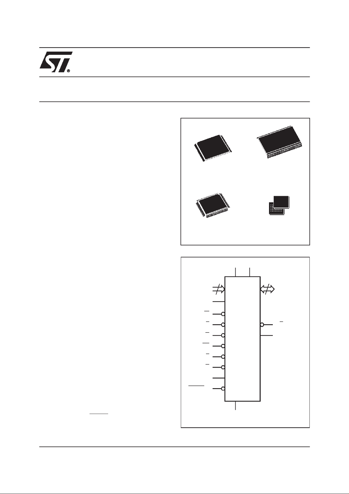
TSOP56 (NF)
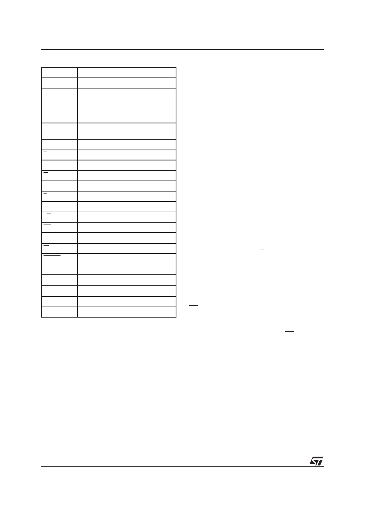
Figure 1. Logic Diagram
V
DD
22
A1-A22
V
PP
W
E
G
RP
M58LW064A
M58LW064B
V
DDQ
TSOP86 II (NH)
FBGA
LBGA54 (ZA)PQFP80 (T)
32
DQ0-DQ31
RB
R
DESCRIPTION
The M58LW064 is a non-volatile Flash memory
that may be erased electrically at the block level
and programmed in-system on a 16 Word or 8
Double-Word basis usinga2.7V to 3.6V supply for
the circuit and a supply down to 1.8V for the Input
WORD
L
B
K
(1)
and Output buffers. TheM58LW064A is organised
as 4M by 16 bit. The M58LW064B has 4M by 16
bit or 2M by 32 bit organisation selectable by the
Word Organisation WORD input. Both devices are
V
SS
internally configured as 64 blocks of 1 Mbit each.
Note: 1. Only on M58LW064B.
May 2000
This is preliminary information on a new product now in development. Details are subject to change without notice.
AI03223
1/53
Page 2
M58LW064A, M58LW064B
Table 1. Signal Names
A1-A22 Address Inputs x16 Organisation
A2-A22 Address inputs x32 Organisation
Data Input/Output x16 and x32
Organisation Command Input,
DQ0-DQ7
DQ8-DQ15
DQ16-DQ31 Data Input/Output x32 Organisation
B Burst Address Advance
E Chip Enable
G Output Enable
K Burst Clock
L Latch Enable
R Valid Data Ready (open drain output)
RB Ready/Busy (open drain output)
RP Reset/Power-down
V
PP
W Write Enable
WORD Word Organisation (M58LW064B only)
V
DD
V
DDQ
V
SS
NC No internal connection
DU Don’t Use (internally connected)
Electronic Signature Output, Block
Protection Ststus Output, Status
Register Output
Data Input/Output x16 and x32
Organisation
Program/Erase Enable
Supply Voltage
Input/Output Supply Voltage
Ground
The devices support Asynchronous Random and
Latch EnableControlledRead withPage mode as
well as Synchronous Burst Read with a configurable burst. They also support pipelined synchronous Burst Read. Writing is Asynchronous or
Asynchronous Latch Enable Controlled.
The configurablesynchronous burst read interface
allows a high data transfer rate controlled by the
Burst Clock K signal. It is capable of bursting fixed
or unlimited lengths of data. The burst type, latency and length are configurable and can be easily
adapted to a large variety of system clockfrequencies and microprocessors. A 16 Word or 8DoubleWord Write Buffer improves effective programming speed by up to 20 times when data is programmed in full buffer increments. Effective Word
programming takes typically 12µs. The array matrix organisation allows each block to be erased
and reprogrammed without affecting other blocks.
Program and Erase operations can be suspended
in order to perform either Read or Program in any
other block and then resumed. All blocks are protected against spurious programming and erase
cycles at power-up. Any block can be separately
protected at any time. The block protection bits
can also be deleted, this is executed as one sequence for all blocks simultaneously. Block protection can be temporarily disabled. Each block can
be programmed and erased over 100,000 cycles.
Block erase is performed in typically 1 second.
An internal Command Interface (C.I.) decodes Instructions to access/modify the memory content.
The Program/Erase Controller (P/E.C.) automatically executes the algorithms taking care of the
timings required by the program and erase operations. Verification is internally performed and a
Status Register tracks thestatus of the operations.
The Ready/Busy output RB indicates the completion of operations.
Instructions are written to the memory through the
Command Interface (C.I.) using standard microprocessor write timings. The device supports the
Common Flash Interface (CFI) command set definition.
A Reset/Power-down mode is entered when the
RP input is Low. In this modethe power consumption is lower than in the normalstandbymode, the
device is write protected and both the Status and
the Burst Configuration Registers are cleared. A
recovery time is required when the RP input goes
High.
The device is offered in various package versions,
TSOP56 (14 x 20 mm), TSOP86 Type II (11.76 x
22.22 mm) and LBGA54 1mm ball pitch for the
M58LW064A and PQFP80 for the M58LW064B.
2/53
Page 3
M58LW064A, M58LW064B
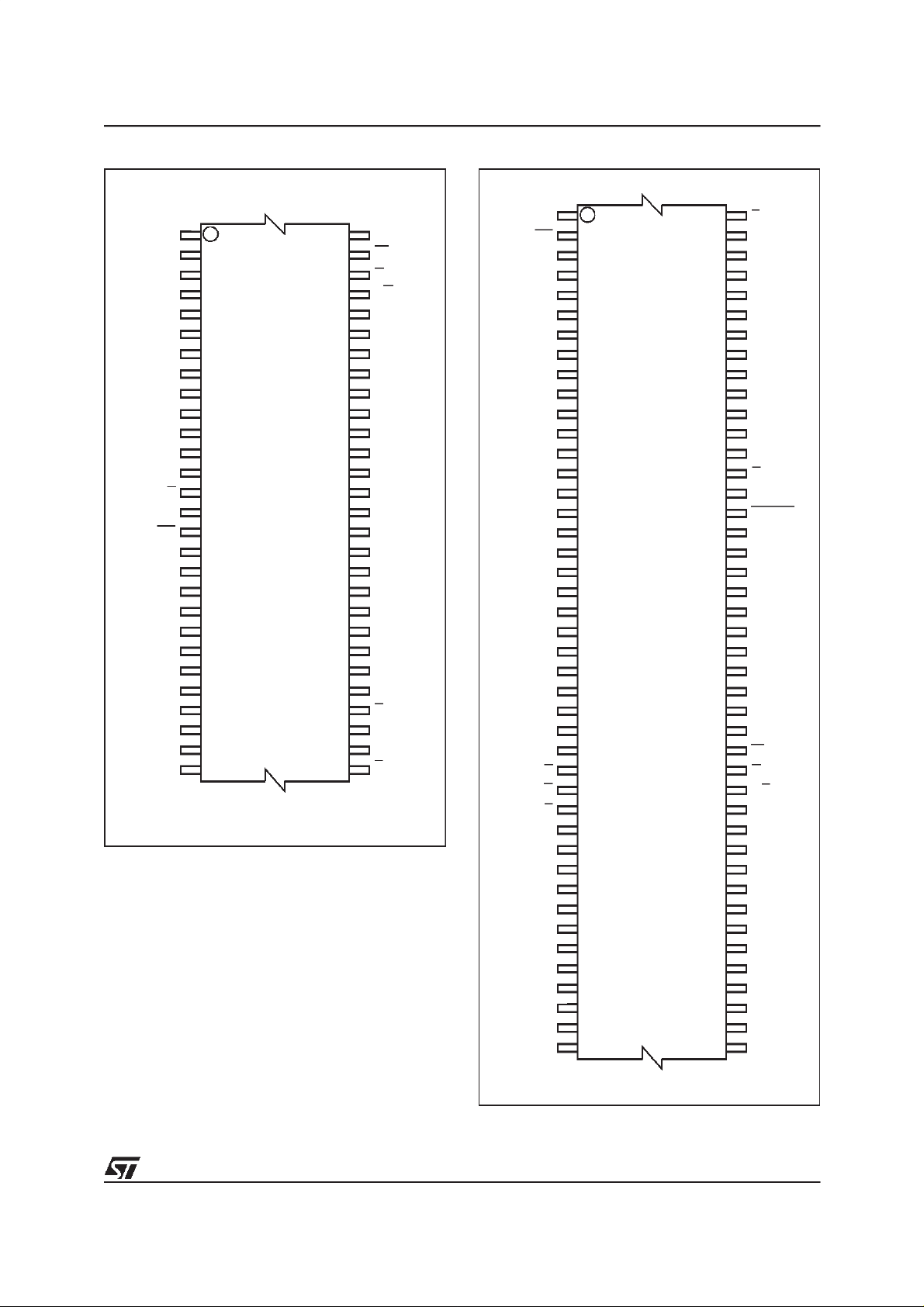
Figure 2. TSOP56 Connections
A22
A21
A20
A19
A18
A17
A16
V
A15
A14
A13
A12
V
A11
A10
V
DD
PP
RP
SS
1
R
14
E
M58LW064A
15
A9
A8
A7
A6
A5
A4
A3
A2
28 29
A1
AI03224
56
43
42
NC
W
G
RB
DQ15
DQ7
DQ14
DQ6
V
SS
DQ13
DQ5
DQ12
DQ4
V
DDQ
V
SS
DQ11
DQ3
DQ10
DQ2
V
DD
DQ9
DQ1
DQ8
DQ0
B
K
NC
L
Figure 3. TSOP86 Type II Connections
V
PP
RP
A11
A10
A9
A8
V
SS
SS
A7
A6
A5
A4
A3
A2
A1
NC
NC
NC
NC
NC
DQ16
DQ24
DQ25
DQ18
DQ26
DQ19
DQ27
DQ0
DQ8
DQ1
DQ9
V
DD
V
DD
DQ2
DQ10
DQ3
DQ11
V
SS
V
SS
1
21
M58LW064A
22
L
K
B
43 44
86
66
65
AI03634
E
A12
A13
A14
A15
V
DD
V
DD
A16V
A17
A18
A19
A20
A21
R
A22
WORD
NC
NC
NC
DQ31
DQ23
DQ30
DQ22DQ17
DQ29
DQ21
DQ28
DQ20
W
G
RB
DQ15
DQ7
DQ14
DQ6
V
SS
V
SS
DQ13
DQ5
DQ12
DQ4
V
DDQ
V
DDQ
V
DDQ
3/53
Page 4
M58LW064A, M58LW064B
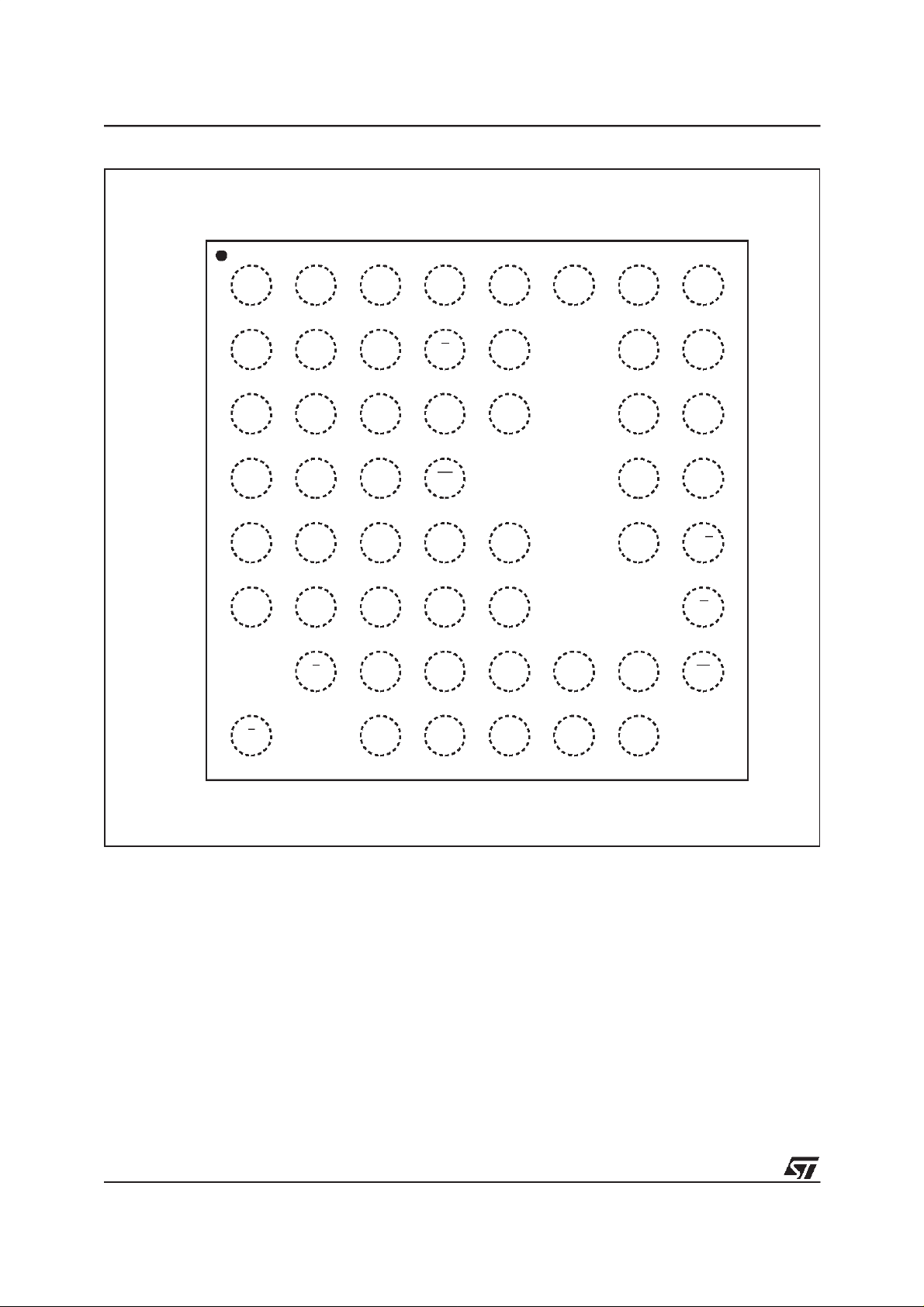
Figure 4. LBGA Connections for M58LW064A (Top view through package)
87654321
A
B RA19A2
C
D A16
E
F
G
A1
A4 A5
K
A6 V
V
SS
A7A3
DQ0
A8
A10 A12
A11
DQ10
DQ2B
PP
EA9
RP
DDQ
A13
A14
A15
DQ5V
V
DD
DQ6
A20
DQ15 R/BDQ9DQ8 DQ1 DQ4DQ3
DQ14
A22A18
A21
A17
GDQ12DQ11
W
4/53
H
L
V
DD
V
SS
DQ13
V
SS
DQ7
AI03536
Page 5
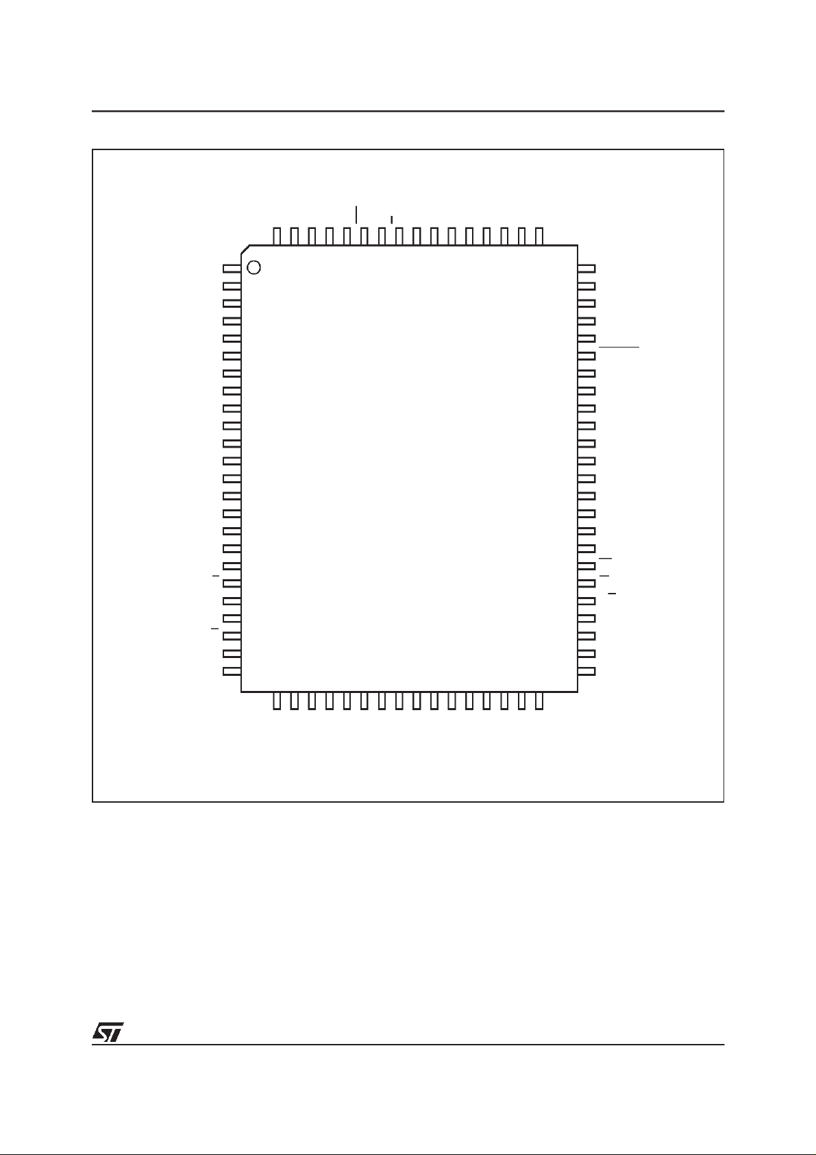
Figure 5. PQFP Connections
M58LW064A, M58LW064B
A7
A6
A5
A4
A3
A2
A1
NC
NC
NC
DQ16
DQ24
DQ17
DQ25
DQ18
DQ26
DQ19
DQ27
NC
DQ0
DQ8
SS
A9
A10
A8
V
1
A11
RP
V
PP
73
A13
E
A12
A14
A15
12 M58LW064B 53
L
K
B
32
DD
V
A16
A17
A18
A19
A20
A21
R
A22
WORD
NC
NC
NC
DQ31
DQ23
DQ30
DQ22
DQ29
DQ21
DQ28
DQ20
W
G
RB
DQ15
DQ7
DQ14
DQ6
DQ1
DQ9
DD
V
DQ2
DQ3
DQ10
SS
V
DQ11
DDQ
V
DDQ
V
DQ4
DQ5
DQ12
VSSV
DQ13
SS
AI03546
5/53
Page 6
M58LW064A, M58LW064B
Table 2. Absolute Maximum Ratings
(1)
Symbol Parameter Value Unit
Grade 1 0 to 70 °C
T
A
T
BIAS
T
STG
V
IO
V
DD,VDDQ
V
HH
Note: 1. Except for the rating ”Operating Temperature Range”, stresses above those listed in the Table ”Absolute Maximum Ratings” may
cause permanent damage to the device. These are stress ratings only and operation of the device at these or any other conditions
above those indicated in the Operating sections of this specification is not implied. Exposure to Absolute Maximum Rating conditions for extended periods may affect device reliability. Refer also to theSTMicroelectronics SURE Program and otherrelevant quality documents.
2. Cumulative time at a high voltage level of 10V should not exceed 80 hours on RP pin.
Ambient Operating Temperature
Grade 6 –40 to 85
Temperature Under Bias –40 to 125 °C
Storage Temperature –55 to 150 °C
Input or Output Voltage
–0.6 to V
DDQ
+0.6
V
Supply Voltage –0.6 to 5.0 V
RP Hardware Block Unlock Voltage
–0.6 to 10
(2)
V
6/53
Page 7
Figure 6. Memory Map
M58LW064A, M58LW064B
M58LW064A,
Word (x16)
Address lines A1-A22
3FFFFFh
3F0000h
01FFFFh
010000h
00FFFFh
000000h
M58LW064B
Organisation
1Mbit or
64 KWords
x64
1Mbit or
64 KWords
1Mbit or
64 KWords
ORGANISATION
Memory control is provided by Chip Enable E,Output Enable G and Write Enable W inputs. A Latch
Enable L input latches an address for both Read
and Write operations. The Burst Clock K and the
Burst Address Advance B inputs synchronize the
memory to the microprocessor during burst read.
Reset/Power-down RP is used to reset all the
memory circuitry, excluding the block protection
bits, andtosetthe chip indeep power down mode.
Erase and Program operations are controlled by
an internal Program/Erase Controller (P/E.C.). A
Status Register data output on DQ7 provides a
Ready/Busy signal to indicate the state of the P/
E.C. operations. A Ready/Busy RB output also indicates the completion of the internal algorithms. A
Valid Data Ready R output indicates the memory
data output valid status during the synchronous
burst mode operations.
A Word Organisation WORD input selects the x16
or x32data width for the M58LW064B. For the x16
only organisation of the M58LW064A or the x16
organisation of the M58LW064B theaddress lines
are A1-A22 and the Data Input/Output is on DQ0DQ15. For the x32 organisation of the
M58LW064B the address lines are A2-A22 and
the Data Input/Output is DQ0-DQ31.
Double-Word (x32)
1FFFFFh
1F8000h
00FFFFh
008000h
007FFFh
000000h
M58LW064B
Address lines
(A1 is Don’t Care)
32 KDouble-Words
32 KDouble-Words
32 KDouble-Words
Organisation
A2-A22
1Mbit or
x64
1Mbit or
1Mbit or
AI03228
MEMORY BLOCKS
The device has a uniform block architecture with
an array of 64 separate blocks of 1Mbit each. The
memory features a software erase suspend of a
block allowing read or programming within any
other block. A suspended erase operation can be
resumed to complete block erasure. A program
suspend operation on a block allows reading only
within any other block. A suspend program operation can be resumedto complete programming.At
any moment of the sequence the Status Register
indicates the status of the operation.
Each block is erased separately. An Erase or Program operation is managed automatically by the
P/E.C. Individual block protection against Program
or Erase provides additional data security. All
blocks are protected during power-up. A software
instruction is provided to cancel all block protection bits simultaneously in an application and a
higher level input on RP can temporarily disable
the protection mechanism. A software instruction
is provided to allow protection of some or all of the
blocks in an application. All Program or Erase operations are blocked when the Program/Erase Enable input VPPis Low.
7/53
Page 8
M58LW064A, M58LW064B
BUS OPERATIONS
The following operations can be performed using
the appropriate bus configuration:
Asynchronous
– Read Array
– Read Electronic Signature
– Read Block Protection
– Read Status Register
– Read Query
– Write
– Output Disable
– Standby
– Reset/Power-down
Synchronous
– Address Latch
– Burst Read
– Burst Read Suspend
– Burst Read Interrupt
– Burst Read Resume
– Burst Address Advance
See Tables 3, 4, 5, 6 and 7.
COMMAND INTERFACE
Instructions, made up of Commands written in Cycles, can be given to the Program/Erase Controller
(P/E.C.) by writing to the Command Interface
(C.I.). At power-up or on exit from power down or
if VDDis lower than V
, the Command Interface
LKO
is resetto Read Array. Any incorrect commandwill
reset the device to Read Array. Anyimproper command sequence will cause the Status Register to
report the error condition and the device will default to Read Status Register.
The internal Program/Erase Controller (P/E.C.)
automatically handles all timing and verification of
the Program and Erase operations. The Status
Register information P/ECS on DQ7 can be read
at any time, during programming or erase, to monitor the progress of the operation.
Table 3. Asynchronous Bus Operations
Operation E G W RP L DQ0-DQ31
Read Array
Read Electronic Signature or
Block Protection Status
Read Status
P/E.C. Active
Read Query
Write V
Output Disable
Standby
Reset/Power-down X X X
Note: 1. X = Don’t Care VILor VIH. High = VIHor VHH.
2. ? = need to check with designers - X or V
V
IL
V
IL
V
IL
V
IL
IL
V
IL
V
IH
(1)
V
IL
V
IL
V
IL
V
IL
V
IH
V
IH
X X High X High Z
???
IL
V
IH
V
IH
V
IH
V
IH
V
V
IH
High X Data Output
High X
High X Status Register Output
High X CFI Query Output
High V
IL
High X High Z
V
IL
IL
X High Z
Manufacturer or Device Code
Output Block Protection Status
Data Input
8/53
Page 9
M58LW064A, M58LW064B
Table 4. Synchronous Burst Read Operations
(1)
Operation E G RP K L B
Address Latch
Burst Read
Burst Read Suspend
Burst Read Interrupt (E)
V
IL
V
IL
V
IL
V
IH
Burst Read Interrupt (RP) X X
Burst Read Resume
Burst Address Advance
No Data Output Burst Address
Advance with valid Data Output
Note: 1. X = Don’t Care, VILor VIH.
2. ? need to check with designers for various X and clock _/ definitions
V
IL
V
IL
V
IL
V
IH
V
IL
V
IH
X
V
IL
V
IH
V
IL
V
IH
V
IH
V
IH
V
IH
V
IL
V
IH
V
IH
V
IH
Table 5. Asynchronous Read Electronic Signature Operation
Code Device E G W A22-A1 A22-A2 DQ7-DQ0
Manufacturer All
M58LW064A
Device
M58LW064B
Note: 1. For M58LW064B, A1 = Dont’Care
(1)
V
IL
V
IL
V
IL
V
IL
V
IL
V
IL
V
V
V
A1-A22
DQ0-DQ31
_/
_/
X
X
V
IL
V
IH
V
IH
V
IH
V
IH
V
IH
V
IH
V
IH
Addess Input
Data Output
High Z
High Z
X X X High Z
_/
_/
_/ V
IH
IH
IH
V
IH
V
IH
IH
00000h 00000h 20h
00001h – 17h
V
IL
V
IL
V
IL
Data Output
High Z
Data Output
– 00001h 14h
Table 6. M58LW064A CFI Block Protection Status Query Operation
(1)
Block Status E G W A1 A2 A3-A16 A17-A22 DQ7-DQ0
Protected
Unprotected
Note: 1. X = Dont’Care, VILor VIH.
V
IL
V
IL
Table 7. M58LW064B CFI Block Protection Status Query Operation
V
IL
V
IL
V
IH
V
IH
V
IH
V
IH
V
IH
V
IH
X Block Address 01h
X Block Address 00h
(1)
Block Status E G W A1 A2 A3 A4-A16 A17-A22 DQ7-DQ0
Protected
Unprotected
Note: 1. X = Dont’Care, VILor VIH.
V
IL
V
IL
V
V
V
IL
IL
IH
V
IH
V
X
V
X
V
IH
IH
IH
V
IH
X Block Address 01h
X Block Address 00h
9/53
Page 10

M58LW064A, M58LW064B
SIGNAL DESCRIPTIONS
See Figure 1 and Table 1.
Address Inputs (A1-A22). A1 is used to select
between the high and low Word in the x16 configuration of the M58LW064A or B. For the
M58LW064B A1 is not used in the x32 mode.
When Chip Enable E is at VILthe address bus is
used to input addresses for the memory array in
Read mode, or addresses for the data to be programmed, or to input addresses associated with
Commands to be written to the Command Interface. Theaddress latch is transparent when Latch
Enable L is at VIL. The address inputs for the
memory array are latched on the rising edge of
Chip Enable E or Latch Enable L or Write Enable
W, whichever occurs first in a writeoperation. The
address is also internally latched in the command
for an Erase or Program Instruction.
Data Inputs/Outputs (DQ0-DQ31). Input data
for a Write to Buffer andProgram operation andfor
writing Commands to the Command Interface are
latched on the rising edge of Write Enable W or
Chip Enable E, whichever occurs first.
When Chip Enable E and Output Enable G are at
VILdata is output from the Array, the Electronic
Signature - the Manufacturer and the Device code
- the Block Protection status, the CFI Query information or the Status Register.The databus is high
impedance when the device is deselected with
Chip Enable E at VIH, Output Enable Gis at VIHor
RP is at VIL. When the P/E.C. is active the Status
Register content is output on DQ0-DQ7 and DQ8DQ31 are at VIL.
Chip Enable (E). The Chip Enable E input activates the memory control logic, input buffers, decoders and sense amplifiers. Chip Enable E at V
IH
deselects thememory and reduces the power consumption to the standby level.
Output Enable (G). The Output Enable G gates
the outputs through the data output buffers during
a read operation. When Output Enable G is at V
IH
the outputs are high impedance. Output Enable G
can be used to suspend the data output in a burst
read operation.
Write Enable (W). The Write Enable W input
controls writing to the Command Interface, Input
Address and Data latches. Both addresses and
data are latched onthe rising edge of W (see also
Latch Enable L).
Reset/Power-down (RP). The Reset/Power-
down RP input provides a hardware reset of the
memory and power-down functions. Reset/Powerdown of the memory is achieved by pulling RP to
VILfor at least t
. Writing is inhibited to protect
PLPH
data, the Command Interface and the P/E.C. are
reset. The Status Register information is cleared
andpower consumptionis reduced to deep powerdown level. The device acts as deselected, that is
the data outputs are high impedance.
When RP rises to VIH, the device will be available
for new operations after a delay of t
PHQV
and will
be configured by default for Asynchronous Random Read. The minimum delay required toaccess
the Command Interface by a write cycle is t
PHWL
If the RP input is activated during a Block Erase, a
Write to Buffer and Program ora Block Protect/Unprotect operation the cycle is aborted and data is
altered and may be corrupted. The Ready/Busy
output RB may remain low for a maximum time of
t
PLPH+tPHRH
beyond the completion of the Reset/
Power-down RP pulse.
Applying the highervoltage VHHtothe Reset/Pow-
er-down input RP temporarily unprotects and enables Erase and Program operations on allblocks.
Thus it acts as a hardware block unprotect input.
In an application, it is recommended to associate
RP to the reset signal of the microprocessor. Otherwise, if a reset operation occurs while the device
is performing an Erase or Program cycle, the
Flash memory may output the Status Register information instead of being re-initialized to the default Asynchronous Random Read.
Latch Enable (L). Latch Enable L latches the address bits A1-A22 on its rising edge for the Asynchronous Latch Enable Controlled Read or Write,
or Synchronous Burst Read operations. The address latch is transparent when Latch Enable L is
at VIL. Latch Enable Lmust remain at VILforAsynchronous Random Read and Write operations.
.
10/53
Page 11

M58LW064A, M58LW064B
Burst Clock (K). The Burst Clock K is used only
in burst mode. It is the fundamental synchronous
signal that allows internal latching of the address
from the address bus, together with Latch Enable
L; increment of the internal address counter in association with Burst Address Advance B;and to indicate valid data on the external data bus. All
these operations are synchronously controlled on
the valid edge of the Burst Clock K, which can be
selected to be the rising or falling edge depending
on the definition in the Burst Configuration Register.
For Asynchronous Read or Write, the Burst Clock
K input level is Don’tCare. For Synchronous Burst
Read the address is latched on the first valid clock
edge when Latch Enable L is at VIL, or the rising
edge of Latch Enable L, whichever occurs first.
Burst Address Advance (B). Burst Address Advance Benables increment of the internal address
counter when it falls to VILduring Synchronous
Burst Read. It is sampled on the last valid edge of
the Burst Clock K at the expiry of the X-latency
time. If sampled at VIL, new data will be output on
the next Burst Clock K valid edge (or second next
depending on the definitionin the Burst Configuration Register). If it is at VIHwhensampled, the previous data remains on the Data Outputs. The Burst
Address Advance B may be tied to VIL.
Ready (R). The Valid Data Ready R is an output
signal used during Synchronous Burst Read. It indicates, at the valid clock edge (or one cycle before depending on the definition in the Burst
Configuration Register), if valid data is ready on
the Data Outputs. New Data Outputs are valid if
Valid Data Ready R is at VIH, the previous Data
Outputs remain active if Valid Data Ready R is at
VIL.
In all operations except Burst Read, Valid Data
Ready R is at VIH. It may be tied to other components with the same Valid Data Ready R signal to
create a unique system Ready signal. The Valid
Data Ready R output has an internalpull-up resistor ofaround 1 MΩ powered from V
, designers
DDQ
should use an external pull-up resistor of the correct value to meet the external timing requirements for R going to VIH.
Word Organisation (WORD). The Word Organisation WORD input is present only on the
M58LW064B and selects x16 or x32 organisation.
The WORD input selects the data width as Word
wide (x16) or Double-Word wide (x32). When
WORD is at VIL, Word-wide x16 width is selected
and data is read and programmedon DQ0-DQ15,
DQ16-DQ31 are at high impedance and A1 is the
LSB address. When WORD is at VIH, the DoubleWord wide x32 width is selected and the data is
read and programmed on DQ0-DQ31, and A2 is
the LSB address.
Ready/Busy (RB). Ready/Busy RB is an opendrain output and gives the internal state of the P/
E.C. When Ready/Busy RB is at VILthe device is
busy with a Program or Erase operation and it will
not accept any additional program or erase instructions except for the Program or Erase Suspend instructions. When a Program or Erase
Suspend is given the RB signal rises to VIH, after
a latency time, to indicate that the Command Interface is ready for a new instruction. When RB is at
VIH, the device is ready for any Read, Program or
Erase operation. Ready/Busy RB is also at V
IH
whenthe memory isin Erase/Program Suspend or
Standby modes.
Program/Erase Enable (VPP). Program/Erase
Enable VPPautomatically protects all blocks from
programming or erasure when at VIL.
Supply Voltage (VDD). The Supply Voltage V
DD
is the main power supply for all operations (Read,
Program and Erase).
Input/Output Supply Voltage (V
put/Output Supply Voltage V
DDQ
). The In-
DDQ
is the Input and
Output buffer power supply for all operations
(Read, Program and Erase).
Ground (VSS). Ground VSSisthe reference for all
the voltage measurements.
11/53
Page 12

M58LW064A, M58LW064B
DEVICE OPERATIONS
See Tables 5, 6, 7 and 10.
Address Latch. An address is latched on the ris-
ing edge of the Latch Enable L input for Asynchronous Latch Enable Controlled Read. For
Asynchrouns Latch Enable Controlled Write, the
address is latched on the rising edge of Chip Enable E, Write Enable W or Latch Enable L, whichever occurs first.
For Synchronous Burst Read the address is
latched on the first valid Burst Clock K edge when
Latch Enable L is at Low, or on the rising edge of
Latch Enable L, whichever occurs first.
Asynchronous Random Read. Asynchronous
Random Read outputs the contents of the Array.
Both Chip Enable E andOutput Enable G must be
Low in order to read the output of the memory.
By first writing the appropriate Instruction, the
Electronic Signature (RSIG), the Status Register
(RSR), the Read Query Instruction (RCFI) or the
Block Protection Status (RSIG) can be read.
Asynchronous Random Read is the default read
mode which the device enters on power-up or on
return fromReset/Power-down.
Asynchronous Page Read. Asynchronous
Page Read may be used for Random or Latch Enable Controlled Reads of the Array, which are performed independent of the Burst Clock signal. A
page has a size of 4 Words or 2 Double-Words
and is addressed by the address inputs A1 and A2
in the x16, or A2 only in the x32 organisation. Data
is read internally and stored in the Page Buffer.
The page read starts when both Chip Enable E
and Output Enable G are Low. The first data is internally read and is output after the normal access
time t
. Successive Words or Double-Words
AVQV
can be read with a much reduced access time of
t
AVQV1
by changing only the low address bits.
Synchronous Burst Read. The memory supports different types of burst access using a Burst
Configuration Register to configure the burst type,
length and latency.
In continuous burst read, one burst read operation
can access the entire memory sequentially by
keeping the Burst Address Advance B Low for the
appropriate number of clock cycles. At the end of
the memory address space the burst read restarts
from the beginning at address 000000h.
Synchronous Burst Read is activated when the
Burst Clock K input is clocking and Chip Enable E
is Low. The burst start address is latched and
loaded into the internal Burst Address Counter on
the valid Burst Clock K edge (rising or falling depending on the M6 bit value for the Burst Clock
Edge Configuration in the Burst Configuration
Register) when Latch Enable Lis Low, orupon the
rising edge of Latch Enable L when the Burst
Clock K is valid. After an initial memory latency
time, the memory outputs data each clock cycle
(or two clock cycles depending onM9 bit value defined in the Burst Configuration Register). The
Burst Address Advance B input controls the memory burst output. The second burst output is on the
next clock valid edge after the Burst Address Advance B has been pulled Low.
The Valid Data Ready output signal R monitors if
the memory burst boundary is exceeded and the
Burst Controller of the microprocessor needs to insert wait states. When Valid Data Ready R is Low
on the active clock edge, no new data is available
and the memory does not increment the internal
address counter at the active clock edge even if
Burst Address Advance B is Low.
Synchronous Burst Read will be suspended when
Burst Address Advance B is High. The Valid Data
Ready signal R may be configured (by bit M8 of
Burst Configuration Register) to be valid immediately at the valid clock edge or one data cyclebefore the valid clock edge.
To increase the data throughput the device has
been built with an internal pipelined architecture
allowing the user to enter a burst read input command and the next starting address location to be
read while the device is filling the output data bus
with its current burst content. This pipelined structure is intended to produce no wait-states on the
output data bus for successive burst read mode
operations.
Asynchronous and Latch Enable Controlled
Write. Asynchronous Write is used to give com-
mands to the Command Interface for Instructions
tothe memory or to latch addressesand input data
to be programmed. To perform any Instruction the
Command Interface is activated starting with a
write cycle. A write cycle is also required give the
Instruction to clear the Status Register information. Two write cycles are needed to define the
Block Erase and the Write to Buffer and Program
Instructions. The first write cycle defines the Instruction selection and the second indicates the
appropriate block address to be erased for the
Block Erase instruction, or the address locations to
program with the number of Words or DoubleWords in the Write to Buffer and Program Instruction.
An Asynchronous Write is initiated when Chip Enable E, Write Enable W and Latch Enable L are
Low with Output Enable G High. Commands and
Input Data are latched on the rising edge of Chip
Enable E or Write Enable W, whichever occurs
first. For an Asynchronous Latch Enable Controlled Write the address is latched on the rising
edge of Latch Enable L, Write Enable W or Chip
Enable E, whichever occurs first.
12/53
Page 13

M58LW064A, M58LW064B
Data to be programmed in the array is internally
latched inthe Write Bufferbefore theprogramming
operation starts and a minimum of 4 Words or 2
Double-Words need to be programmed in the
same sequence and must be contained in the
same address location boundary defined by A1 to
A2 for the x16 and A2 for the x32 organisation.
Write operations are asynchronous and the Burst
Clock signal K is ignored during a write operation.
Output Disable. The data outputs are high impedance when the Output Enable G is High.
Standby. The memory is in standby when Chip
Enable E goes High and the P/E.C. is idle. The
power consumption is reduced tothe standby level
and the outputs are high impedance, independent
of the Output Enable G or Write Enable W inputs.
Automatic Low Power. After a short time of bus
inactivity (no Chip Enable E, Latch Enable L or Address transitions) the chip automatically enters a
pseudo-standby mode where consumption is reduced to the Automatic Low Power standby value,
while theoutputs may still drive the bus. The Automatic Low Power feature is available only for
Asynchronous Read.
Power-down. The memory is in Power-down
when Reset/Power-down RP is Low. The power
consumption is reduced to the power-down level
and the outputs are high impedance, independent
of the Chip Enable E, Output Enable G or Write
Enable W inputs.
Electronic Signature. Two codes identifying the
manufacturer and the device can be read from the
memory allowing programming equipment or applications to automatically match their interface to
the characteristics of the memory. The Electronic
Signature is output by givingthe RSIG Instruction.
The manufacturer code is output when all the Address inputs are Low. The device code is output
when A1 (M58LW064A) or A2 (M58LW064B) input is High, the other pins A3-A22 must be Low.
The codes are output on DQ0-DQ7. A return to
Read mode is achieved by writing the Read Array
instruction.
INITIALIZATION
The device must be powered up and initialized in
a predefined manner. Procedures other than
specified may result in undefined operation.
Power should be applied simultaneously to V
and V
with the RP input held Low. When the
DDQ
DD
supplies are stable RP is taken High. The Output
Enable G, Chip Enable E and Write Enable W inputs should also be held High during power-up.
The memory will be ready to accept the first Instruction after the power-up time t
. The device
PUR
is automatically configured for Asynchronous Random Read at power-up or after leaving Reset/
Power-down.
BURST CONFIGURATION REGISTER
See Tables 8, 9, 10 and 11.
The Synchronous Burst Read, Asynchronous
Random Read, Asynchronous Latch Enable Controlled Read are selected using the Burst Configuration Register.
For Synchronous Read the register defines the X
and Y Latencies, Valid Data Ready signal timing,
Burst Type, Valid Clock Edge and Burst Length.
The Burst Configuration Register is programmed
usingthe SetBurst Configuration Register (SBCR)
Instruction and will retain the stored information
until it is programmed again or the device is reset
or goes into the Reset/Power-down.
The Burst Configuration Register bits M2-M0
specify the burst length (1, 2, 4, 8 or continuous);
bit M3 specifies Asynchronous Random Read or
Asynchronous Latch Enable Controlled Read; bits
M4and M5 are not used; bit M6 specifies the rising
or falling burst clock edge as valid; bit M7 specifies
the burst type (Sequential or Interleaved); M8
specifies the Valid Data Ready output period; bit
M9 specifies the Y-latency; bit M10 is not used;
M14-M11 specify the X-latency; and bit M15 selects between Synchronous Burst Read or Asynchronous Read. M10, M5 and M4 are reserved for
future use.
M15 Read Select
The device features three kinds of read operation:
Asynchronous Random Read, Asynchronous
Latch Enable Controlled Read and Synchronous
Burst Read. Page Read may be used in either of
the Asynchronous Read operations.
The Burst Configuration Register bit M15 selects
between Synchronous Burst and Asynchronous
Read.
M14 - M11 and M9 X and Y Latency.
The values of X and Y are used to define the burst
latency for the data sequence. The X-latency defines the number of clock cycles before the output
of the first data from the clock edge that latches
the address. The X-latency can be set from 7 to
16. A value of 7 is only valid for continuous burst.
The Y-latency is the number of clock cycles need-
ed to output the next data from the burst register,
following the first data output. The latency can be
set to 1 or 2 clock cycles.
The minimum X-Latency value to consider depends on the Burst Clock K signal frequency. The
burst performance in terms of frequency is listed in
Table 11 and indicates theminimum X-latencyand
Y-latency values (X.Y.Y.Y) related to the burst
type, burst length and x16 or x32 organisation.
13/53
Page 14

M58LW064A, M58LW064B
M8 Valid Data Ready R Signal Configuration.
The Valid Data Ready R output signal indicates
when valid data is on the data outputs synchronous with the valid burst clock egde. It can be asserted by the device synchronously with the valid
clock edge or one clock cycle before.
M7 Burst Type.
Accesses within a given burst may be programmed to be either Sequential or Interleaved.
This is referred to as the burst type and is selected
by theBurst Configuration Register M7 bit. The access order within a burst is determined by the
burst length, the burst type and the starting address (See Table 8).
M6 Valid Clock Edge Configuration.
All the synchronous operations such as Burst
Read, Output Data or Ready signal validation can
be synchronized on the valid rising or on the falling
edge of the Burst Clock signal K.
M2 - M0 Burst Length.
Synchronous reads have a programmable burst
length, set using the M2- M0 bits of the Burst Configuration Register. The burst length corresponds
to the maximum number of Words or DoubleWords that can be output. Burst lengths of 1, 2, 4
or 8 are available for both the Sequential and Interleaved burst types, and a continuous burst is
available for the Sequential type. The burst length
of 8 is not available in the x32 configuration.
When a Read command is issued, a block of
Words or Double-Words equal to the burst length
is selected. All accesses for that burst take place
within this block, meaning that the burst wraps
within the burst block if a boundary is reached.
If a Continuous Burst Read has been initiated the
device will output data synchronously. Depending
on the starting address of the read, the device activates the Valid Data Ready R output to indicate
that it needs a delay to complete the internal read
operation before outputing data. If the startingaddress is aligned to a four Word boundary the continuous burst mode will run without activating the
Valid Data Ready R output. If the starting address
is not aligned to a four Word boundary,Valid Data
Ready R is activated at the beginning of the continuous burst read to indicate that the device
needs an internal delay to read the content of the
four successive words in the array.
Pipelined Burst Read.
An overlapping Burst Read operation is possible.
That is, the address and data phases of consecutive synchronous read operations can be overlapped by several clock cycles. This is done by
applying a pulse on Latch Enable Linput to latch a
new address before the completion of the data
output of the current cycle. This reduces or avoids
wait-states in the data output for the burst read
mode. The minimum clock edge number for the
following read sequence must be six before the
last data output of the previous read cycle. The
pipelined burst read mode is available in the x16
organisation for both burst length definitions of
four and eight, and in the x32 organisation for the
burst length of four. It is not possible for a burst
length of one or two.
14/53
Page 15
Table 8. Burst Type Definition (x16 mode)
Starting Address
Burst Length
2
4
8
(binary)
A3-A2-A1
0-0-0 0-1 0-1
0-0-1 1-0 1-0
0-0-0 0-1-2-3 0-1-2-3
0-0-1 1-2-3-0 1-0-3-2
0-1-0 2-3-0-1 2-3-0-1
0-1-1 3-0-1-2 3-2-1-0
0-0-0 0-1-2-3-4-5-6-7 0-1-2-3-4-5-6-7
0-0-1 1-2-3-4-5-6-7-0 1-0-3-2-5-4-7-6
0-1-0 2-3-4-5-6-7-0-1 2-3-0-1-6-7-4-5
0-1-1 3-4-5-6-7-0-1-2 3-2-1-0-7-6-5-4
1-0-0 4-5-6-7-0-1-2-3 4-5-6-7-0-1-2-3
1-0-1 5-6-7-0-1-2-3-4 5-4-7-6-1-0-3-2
1-1-0 6-7-0-1-2-3-4-5 6-7-4-5-2-3-0-1
1-1-1 7-0-1-2-3-4-5-6 7-6-5-4-3-2-1-0
Sequential
(decimal)
M58LW064A, M58LW064B
Interleaved
(decimal)
Table 9. Burst Type Definition (x32 mode)
Starting Address
Burst Length
2
4
(binary)
A2-A1
0-0 0-1 0-1
0-1 1-0 1-0
0-0 0-1-2-3 0-1-2-3
0-1 1-2-3-0 1-0-3-2
1-0 2-3-0-1 2-3-0-1
1-1 3-0-1-2 3-2-1-0
Sequential
(decimal)
Interleaved
(decimal)
15/53
Page 16
M58LW064A, M58LW064B
Table 10. Burst Configuration Register
(1)
BCR mode bit Description Value Description
0 Synchronous Burst Read
M15 Read Select
1 Asynchronous Read
0001 Reserved
(5)
(6)
(7)
(8)
M14-M11
M9
X-Latency
Y-Latency
(4)
(4)
0010
0011
7, only for F
8, only for F
0100 9, only for F
0101
0110
1001
1010
1011
1101
10, only for F
11, only for F
12, only for F
13, only for F
14, only for F
16, only for F
= 33MHz
K
= 33MHz
K
= 33MHz
K
= 50MHz
K
= 50MHz
K
= 50MHz
K
= 50MHz
K
= 66MHz
K
= 66MHz
K
0 One Burst Clock cycle
1 Two Burst Clock cycles
0 R valid Low during valid Burst Clock edge
M8 Valid Data Ready
1 R valid Low one data cycle before valid Burst Clock edge
0 Interleaved
M7 Burst Type
1 Sequential
0 Falling Burst Clock edge
M6 Valid Clock Edge
1 Rising Burst Clock edge
0 Random Read
M3 Asynchronous
1 Latch Enable Controlled Read
100 1 Word or Double-Word
101 2 Words or Double-Words
M2-M0
Burst Length
(2)
001 4 Words or Double-Words
010
8 Words or Double-Words
(3)
111 Continuous
Note: 1. The BCR defines both the read mode and the burst configuration.
2. Synchronous burst length is defined as Word or Double-Word, the data bus width depends only on the WORD input.
Asynchronous Page read is two Words or one Double-Word.
3. A burst length of 8 is not available for x32 organisation.
> 50MHz when X-Latency = 10 or 12, Y-Latency = 2 independent of the value of M9.
4. At F
K
= 66MHz when X-Lantency = 14 or 16, Y-Latency = 2 indepedent of the value of M9.
At F
K
5. Latency 7 valid only for continuous burst. Otherwisw Latency = 8.
6. Latency 10 valid only for continuous burst. Otherwisw Latency = 12.
7. Latency 11 valid only for continuous burst. Otherwisw Latency = 12.
8. Latency 14 valid only for continuous burst. Otherwisw Latency = 16.
16/53
Page 17

M58LW064A, M58LW064B
Table 11. Burst Performance
x16 organisation x32organisation
Sequential Interleaved Sequential Interleaved V
Burst length:
1,2,4,8
8.1.1.1 8.1.1.1 8.1.1.1 8.1.1.1 7.1.1.1 7.1.1.1 ≤ 33 MHz
12.1.1.1 12.1.1.1 12.1.1.1 12.1.1.1 10.1.1.1 10.1.1.1 ≤ 50 MHz
t.b.a. t.b.a. t.b.a. t.b.a. t.b.a. t.b.a. ≤ 60 MHz
16.2.2.2 16.2.2.2 16.2.2.2 16.2.2.2 14.2.2.2 14.2.2.2 ≤ 66 MHz
Note: 1. The burst length of 8 is not available in the x32 organisation.
Burst length:
1,2,4,8
(1)
X-Y Latencies (minimum)
Burst length:
1,2,4
Burst length:
1,2,4
x16
organisation
= 2.7 to 3.6V
DD
Continuous Burst
x32
organisation
Clock
Frequency
17/53
Page 18

M58LW064A, M58LW064B
INSTRUCTIONS AND COMMANDS
The Command Interface latches commands written to the memory. Instructions are made up of
one or more commands to perform:
– Read Array (RD),
– Read Electronic Signature or Read Block Pro-
tection (RSIG),
– Read Status Register (RSR),
– Read Query (RCFI),
– Clear Status Register (CLRS),
– Block Erase (EE),
– Write to Buffer and Program (WBPR),
– Erase/Program Suspend (PES),
– Erase/Program Resume (PER),
– Set Burst Configuration Register (SBCR),
– Block Protect (BP), and
– Block Unprotect (BU).
Instructions (see Table 12)are composed of a first
write sequence followed by either a second write
sequence needed toconfirm an Erase or Program
instruction or by a read operation in order to read
data from the array, the Electronic Signature, the
Block Protection information, the CFI or the Status
Register information. The instructions for Write to
Buffer and Program and Block Erase operations
consist of two commands written into the memory
Command Interface (C.I.) that start the automatic
P/E.C. operation. Erasure of a memory block may
be suspended,in order to read data fromor to program data in an other block, andthen be resumed.
Write to Buffer and Program operation may be
suspended, in order to read data from another
block, and then be resumed.
At power-up the Command Interface is reset to
Read Array. The appropriate Instruction must be
given to access Read Query (RCFI), Read Electronic Signature or Block Protection Status (RSIG)
or Read Status Register (RSR). Reading of the
memory array is disabled during a Block Protect/
Unprotect (BP, BU), a Block Erase (EE) or a Write
to Buffer and Program (WBPR) Instruction. A
Erase/Program Suspend Instruction (PES) must
be given to read under these conditions.
Read Array Instruction (RD). The Read Array
Instruction consists of one write cycle giving the
command FFh. Subsequent read operations will
read the array content addressed and output the
corresponding data. The Read Array Instruction
remains active until another one is written into the
Command Interface. At Power-up or at the exit of
the Reset/Power-down mode, the device is by default initialised to Read Array.
Read Electronic Signature Instruction (RSIG).
An Electronic Signature can be read from the
memory allowing programming equipment or applications to automatically match their interface to
the characteristics of the device.
The Electronic Signature instruction consists of a
first write cycle giving the command 90h, followed
by a subsequent read which will output the Manufacturer Code, the Device Code or the Block Protection Status. The Manufacturer Code is output
when all the address inputs are at VIL. The Device
Code is output when A1 (for the M58LW064A) or
A2 (for the M58LW064B) is at VIH, with all other
address inputs at VIL. The code is output on DQ0DQ7 with DQ8-DQ31 at VIL.
The RSIG Instruction also allows access to the
Block Protection Status for the selected block address defined by A17-A22. After the Read Electronic Signature (RSIG) command, A1-A2 (for the
M58LW064A) or A2-A3 (for the M58LW064B) are
set to VIH, while A17-A22 define the address of the
block to be queried. A read operation outputs 01h
if the block is protected and 00h if the block is not
protected.
Read Query Instruction (RCFI). The ReadQuery Instruction is initiated with one write cycle giving
the command 98h at any address. Subsequent
read operations, depending on the address specified, will output the Block Status information, the
Common Flash Interface ID string, the System Interface information, the Device Geometry Configuration or STMicroelectronics Specific Query
information. The address mappingfor the information is shown in Table 14.
Read Status Register Instruction (RSR). The
Read Status Register Instruction consists of one
write cycle giving the command 70h. Subsequent
read operations, independent of the address, output the Status Register informationthat indicates if
a Block Erase, Write to Buffer and Program, Block
Protect or Block Unprotect operation has been
completed successfully. See Table 12. Once initiated the RSR Instruction is active until another
command is given to the Command Interface.
For Asynchronous Read, the Status Register information is present on the output data bus when
both Chip Enable E and OutputEnable G are Low.
InSynchronous Burst Read the Status Register information is output on the data bus DQ1-DQ7
when Latch Enable L goes High or on a valid Burst
Clock K edge (M6 in the Burst Configuration Register specifies the rising or falling valid clock edge)
when Latch Enable L is low. An interactive update
of the status register information is possible by
toggling Output Enable G, or when the device is
18/53
Page 19

Table 12. Instructions
Mne-
monic
Instruction Cycles
M58LW064A, M58LW064B
1st Cycle 2nd Cycle
Comments
Op. Address Data Op. Address Data
RD
Read Array
Read
Manufacturer
RSIG
Code
Read Device
Code or Block
RSIG
Protection
Status
Read Status
RSR
Register
RCFI Read Query ≥ 2 Write X 98h Read QAh QDh
Clear Status
CLRS
Register
Block
EE
Erase
Write
PES
PER
to Buffer and
Program
Erase/
Program
Suspend
Erase/
Program
Resume
WBPR
1+ Write X FFh
≥ 2 Write X 90h Read 000000h 20h Read Manufacturer Code
≥ 2 Write X 90h Read
2 Write X 70h Read X SRDh
1 Write X 50h
2 Write X 20h Write BAh D0h
≥ 2 Write BAh E8h Write BAh N
1 Write X B0h
1 Write X D0h
IAh IDh
Read Array until a new
write cycle is initiated
Read Device ID Code
SRD = Status Register
Data
QA = Query Address
QD = Query Data
BA = Block Address to
erase
BA = Block Address
N = Word/Double-Word
Count Argument
Confirm command for
Write to Buffer and
Program instruction
Set Burst
Configuration
SBCR
Register
BP Block Protect 2 Write BAh 60h Write BAh 01h
Block
BU
Unprotect
dis-activated by Chip Enable E High and then reactivated by Chip Enable E and Output Enable G
Low, during an Erase or Program operation. The
content of Status Register may also be read atthe
completion of an Erase/Program and/or Suspend
2 Write BCRh 60h Write BCRh 03h
2 Write X 60h Write X D0h
operation.During a Block Erase, Write to Buffer
and Program, Block Protect or Block Unprotect Instruction, DQ7 indicates the P/E.C. status. Itis valid until the operation is completed or suspended,
DQ0-DQ7 output the Status Register content and
DQ8-DQ31 are Low.
BCR =Burst Configuration
Register
Keep the Block Protect bit
active of the selected
block
BA = Block Address
Clear all the Block protect
bits simultaneously
19/53
Page 20

M58LW064A, M58LW064B
Table 13. Status Register Definition
Mnemonic DQ Function Status
P/ECS DQ7 P/E.C. Status
ESS DQ6 Erase Suspend Status
ES DQ5
PS DQ4
Erase/Block Unprotect Status
Write to Buffer and Program/Block
Protect Status
(7)
(7)
DQ3 Not used
PSS DQ2 Program Suspend Status
EPPB DQ1
Erase/Write to Buffer and Program in a
Protected Block
DQ0 Not used
Note: 1. DQ0-DQ6 are High Impedance when DQ7 is indicating that the part is busy. Status Register P/ECS bit7 indicates the P/E.C.status,
check during Program or Erase, and on completion before checking bit4 or bit5 for Program or Erase Success.
2. DQ6 indicates the Erase Suspend Status. On an Erase Suspend instruction P/ECS and ESS bits are set to ’1’. ESS bit remains ’1’
until an EraseResume instruction is given.
3. Erase Status, ES bit5 is set to ’1’ if the P/E.C.has applied the maximum number of erase pulses to the block without achieving an
erase verify.
4. Program Status, PS bit4 is set to’1’ if the P/E.C.has failed to program a Word or Double-Word.
5. DQ2 indicates the Program Suspend Status. On a Program Suspend instruction P/ECS and PSS bits are set to ’1’.PSS bit remains
’1’until an Program Resume instruction is given.
6. DQ1 defines the status of an Erase or Write to Buffer and Program instruction defined in a protected block. RP pin must be held at
to temporarily override the block protect feature once it has been enabled.
V
HH
7. DQ5 and DQ4 simultaneously at ’1’ after an Erase or Block Unprotect instruction indicates that an improper command was entered.
1 = Ready
0 = Busy
(1)
1 = Block Erase Suspended
0 = Block Erase in Progress/Completed
(2)
1 = Error in Block Erase operation or Block
Unprotect
0 = Successful Block Erase operation or Block
Unprotect
(3)
1 = Error in Write to Buffer and Program, Block
(4)
Protect
0 = Write to Buffer and Program, Block Protect
Completed successfully
1 = Program Suspended
0 = Program operation in Progress/Completed
1 = Error in the defined operation
0 = Operation in Progress/Completed
(6)
(5)
20/53
Page 21

M58LW064A, M58LW064B
Clear Status Register Instruction (CLRS). The
Clear Status Register Instruction is given with the
command 50h at any address location. It is a reset
instruction that resets DQ5, DQ4 and DQ1 in the
Status Registerto ’0’.
If an operation such as Block Erase, Write toBuffer and Program Block Protect or Block Unprotect
has failed, the P/E.C.will set DQ5, DQ4 or DQ1 to
’1’ depending on the failure detected (see Table
12, Status Register Definition). The Clear Status
Register Instruction must be given before restarting any corrective Erase/Program Instruction. The
CLRS Instruction should be given also after an
Erase or Program Suspend Instruction failure or
before a Resume Instruction if the previous instruction has been detected to have failed. It is
also a software reset solution that may allow the
execution of several operations such as cumulated Erase or Block Protect operations of multiple
blocks. The Clear Status Register instruction is
valid when the P/E.C. is inactive or the device is in
a suspend mode and it is also valid independent of
the voltage VIHor VHHapplied on the RP input.
Write to Buffer and Program Instruction (WBPR). The Write to Buffer and Program Instruction
is used to program the memory array. Up to 16
Words or 8 Double-Words can be loaded into the
Write Buffer and programmed into the device. The
Write to buffer and Program Instruction is composed of three successive steps. The first step is
to give the Write to Buffer andProgram command,
E8h with the selected memory Block Address
where the program operation should occur. The
Status Register DQ7 bit then indicates the ”buffer
available” status.If the write buffer is not available
(indicated by DQ7 = 0) then the software can either continue monitoring DQ7 until it transitions to
1, or else re-try later by reloading first the WBPR
command, E8h, and then again monitoring the value of DQ7.
Once the ”write buffer available” condition is valid
(indicated by DQ7 = 1), the second step is towrite
the block address again, along with the value N,
where N+1 is the number of Words (x16 organisation) or Double-Words (x32 organisation) to be
programmed.
In the third step, a sequence of N+1 write cycles
loads the addresses and data to the write buffer
(see boundary constraints below). The addresses
must lie between the starting address and the
starting address + (N+1).
The array must be programmed in 4 Word or 2
Double-Word blocks, which must be aligned with
an A2 = A1 = 0 starting address (or A2 = 0 for x32
organisation). Invalid data will be flagged and the
operation will abort with the status register bits
DQ4 and DQ5 set to 1.
The Confirm Command, D0h (the same as Erase/
Program Resume PER Instruction) needs to be
givenimmediately after the completion of the Write
to Buffer and Program Instruction. It represents
the last (that is the N+2) write operation.
The P/E.C. is enabled only if the whole previous
sequence is fully respected. Otherwise an Invalid
Command/Sequence error will be generated with
the Status Register DQ5 and DQ4 set to ’1’. For
additional Write to Buffer and Program operations,
after the initial input command the software can
check the availability of the write buffer by checking DQ7 status from the Status Register.
If an error appears during a program sequence,
the device will stop its operation and DQ4 of the
Status Register will be set to ’1’ to indicate a program failure. DQ5 will indicate if an error has been
detected during a Block Erase operation. If these
bits, DQ4 or DQ5 are set to ’1’,the Write to Buffer
and Program input command is not accepted by
the device until the status register has been
cleared.
Additionally, if the Block is protected and
VIH<RP<VHHinstead of RP = VHH, the Write to
Buffer and Program Instruction will not be accepted by the device, and DQ4 and DQ1 of the status
register will be set to ’1’.
Block Protect Instruction (BP). The Block Protect Instruction BP uses a two-cycle write sequence. The first write cycle gives the command
60h at any address location. The second write cycle gives the block address memorylocation to be
protected and the command 01h.
Block protection can be cleared with the BU Instruction, which unprotects all blocks. Alternatively, temporary unprotect can be achieved by raising
the RP input to VHHand holding it at that level
throughout the Block Erase or Write to Buffer and
Program operations.
21/53
Page 22

M58LW064A, M58LW064B
Block Unprotect Instruction (BU). The Block
Unprotect Instruction BU uses a two-cycle write
sequence. All the Block Protect bits are simultaneously erased. The Block Protect bit register is
erased by giving the command 60h and then the
Confirm command D0h, at any address location.
The sequence is aborted if the Confirm command
is not given and the device will output the Status
Register Data with DQ4 and DQ5 set to ’1’.
Block Erase Instruction (EE). The Block Erase
Instruction EE uses a two-cycle command sequence. The Erase Setup command 20h is written
to any address location. Then a second writecycle
is given with the block address to be erased and
the Confirm command D0h. The sequence is
aborted if the Confirm command is not given and
the device willoutput the StatusRegister Data with
DQ4 and DQ5 set to ’1’.
During the execution of the erase cycle by the P/
E.C., the memory accepts only the Erase/Program
Suspend instructions. Read operations output the
Status Register bits. A complete state of the erase
operation is given by the Status Register bits.
Erase/Program Suspend Instruction (PES).
The Block Erase or Write to Buffer and Program
operations may be suspended by writing the command B0h at any address. The Erase/Program
Suspend Instruction interrupts the P/E.C. Erase or
Program sequence at a predetermined point in the
algorithm. After the Suspend command is written
the device outputs the Status Register data.
It is possible to read or program data in a block
other thanthe one in whichthe Erase Suspend operation is effective. It is only possible to read in a
block other than the one in which a Program Suspend operation is effective. The suspended Erase/
Program operation has to be resumed in order to
complete the previous erase/program sequence.
The Erase Suspend instruction is accepted only
during a Block Erase operation execution. Program Suspend also is valid only during the Writeto
Buffer and Program instruction execution. Block
Erase or Erase/Program Suspend instructions are
ignored if the memory is already in the Suspend
mode.
The Suspend Instruction may be presented atany
time during the execution of a Block Erase. For a
Write to Buffer and Program instruction the Suspend Instruction is accepted only when the P/E.C.
is running.
The device outputs information about thesuspend
in the Status Register information on DQ7, DQ6
and DQ2. If the operation has been completed
DQ7 = ’1’ and DQ6 = ’0’ (Erase Suspend) or
DQ2 = ’0’(Program Suspend).
If the Suspend instruction occurred after the P/
E.C. has completed its operation (DQ7 = 1,
DQ6 = 0 and DQ2 = 0), the Status Register information remains available by toggling Output Enable G. No command is accepted by the device
with the exception of a Read Memory Array Instruction FFh. After the FFh Command is issued,
the device is ready for Read Array (in the mode
defined by the last Set Configuration Register issued).
When a program operation is completed inside a
Block Erase Suspend Instruction, Read Array Instruction FFh will reset the device to Read Array.
The Erase Resume Instruction has to be issued to
complete the whole sequence.
When erase is suspended, the memory will respond only to the Read Array, Read Electronic
Signature, Read Query, Read Status Register,
Clear Status Register, Erase/Program Resume
and the Write to Buffer and Program instructions.
When a Write to Buffer and Program instruction is
suspended, the memory will respond only to the
Read Array, Read Electronic Signature, Read
Query, Read Status Register, Clear Status Register and Erase/Program Resume instructions.
Erase/Program Resume Instruction (PER). If
an Erase Suspend instruction was previously executed, the erase operation may be resumed by
giving the command D0h, at any address. This
also serves as the Confirm command for the Write
to Buffer and Program (WPBR) Instruction which
is issued after the write buffer loading sequence is
completed, and which starts the P/E.C.
22/53
Page 23

M58LW064A, M58LW064B
Set Burst Configuration Register (SBCR).
This instruction uses two command cycles. The
Burst Configuration Setup command 60h is written
with the address corresponding to the Set Burst
Configuration Register content. Then in the second write cycle the address bus A2-A17 specifies
the BCR, Burst Configuration Register, information and the command 03h. The burst length, type,
latency, synchronous/asynchronous read mode
and clock edge active configuration are defined in
that operation. After the command 03h the device
will default in the Read array mode.
Status Register Bits. The P/E.C. status is indicated during execution with a Ready/Busy output
available on DQ7. Any read attempt during Program or Erase command execution will automatically update the Status Register bits. The P/E.C.
automatically sets bits DQ1, DQ2, DQ4, DQ5,
DQ6 and DQ7. The bit DQ0 is reserved for future
use and should be masked. It is not necessary to
specify an address when the Status Register bits
are read. The Status Register is a static memory
register that is reset when RP signalis active or on
a power-down operation.
POWER SUPPLY
Power Down. The memory provides Reset/Pow-
er-down control using the input RP. When Reset/
Power-down RP is pulled to VIL the supply current
drops to typically lessthan 1µA, the memory isdeselected and the outputs are at high impedance. If
RP is pulled to VILduring a Program or Erase operation, this operation is aborted after a latency
time of t
and the memory content is no longer
PLRH
valid.
RESET, POWER-DOWN AND POWER-UP
See Fig 16.
The device is reset if the Reset/Power-down RP
input is pulled to VILfor longer than tPLPH. If the
device was in a Read mode then it will recover
from reset after a time of t
to give valid data
PHQV
output. If the device was executing an Erase or
Program operation, with the P/E.C. active, the operation will abort in a time of t
maximum. The
PLRH
device will be ready to accept new write commends after a time of t
The supply voltages VDDand V
a time t
VDHEL
or t
VDHWL
PHWL
or t
.
PHEL
must be high
DDQ
before a read or write cycle. At first power up Reset/Power-down should be
held Low for a time of t
VDHPH
after VDDand V
DDQ
are high.The device will be ready to accept its first
read or write commands after a time of t
t
.
PUW
PUR
or
COMMON FLASH INTERFACE - CFI
The introduction to the JEDEC CFI specification
Rel. 1.2 quotes, ”The Common Flash Interface
(CFI) specification outlines a device and host system software interrogation handshake which allows specific software algorithms to be used for
entire families of devices. This allows device-independent, JEDEC, ID independent and forwardand backward-compatible software support for the
specified flash device families. It allows flash vendors to standardize their existing interfaces for
long-term compatibility.”
The CFI Query instructionRCFIdescribes how the
device enters the CFI Query mode which enables
information to be read from the Flash memory. CFI
allows a system software to query the flash device
to determine various electrical and timing parameters, density information and functions supported
by the device. CFI allows the system to easily interface to the flash memory, to learn about its features and parameters, enabling the software to
upgrade itself when necessary.
Query Structure Overview
The flash memory displays the CFI data structure
when the CFI Query Instruction RCFI is issued. A
list of the main subsections is detailed in Tables15
to 19.
23/53
Page 24

M58LW064A, M58LW064B
Table 14. Query Structure Overview
Offset Sub-section Name Description
00h Manufacturer Code
01h Device Code
10h CFI Query Identification String Command set ID and algorithm data offset
1Bh System Interface Information Device timing and voltage information
27h Device Geometry Definition Flash device layout
P(h) Primary Algorithm-specific Extended Query table
A(h) Alternate Algorithm-specific Extended Query table
(BA+3)h Block Status Register Block-related Information
Table 15. CFI - Query Address and Data Output in the x16/x32 organization
Address
A22-A1 (M58LW064A)
A22-A2 (M58LW064B)
Note: 1. The x8 or Byte Address mode is not available.
2. In the x16 organization, the value of the address location of the CFI Query is independent of A1 pad (M58LW064B).
3. Query Data are always presented on the lowest order data outputs (DQ7-DQ0) only. Others data (DQ31-DQ8) are set to ’0’.
4. For M58LW064B, A1 = Don’t Care.
(4)
Data Instruction
10h 51h ”Q”
11h 52h ”R”
12h 59h ”Y”
13h 20h
14h 00h
15h 31h
16h 00h
17h 00h
18h 00h
19h 31h
1Ah 00h
Query ASCII String 52h; ”R”
Primary Vendor:
Command Set and Control Interface ID Code
Primary algorithm extended Query Address Table:P(h)
Alternate Vendor:
Command Set and Control Interface ID Code
Alternate Algorithm Extended Query address Table
Additional information specific to the Primary
Algorithm (optional)
Additional information specific to the Alternate
Algorithm (optional)
51h; ”Q”
59h; ”Y”
24/53
Page 25

M58LW064A, M58LW064B
Table 16. CFI - Device Voltage and Timing Specification
Address
A22-A1 (M58LW064A)
A22-A2 (M58LW064B)
Note: 1. Bits are coded in Binary Code Decimal, bit7 to bit4 are scaled in Volt and bit3 to bit0 in mV.
2. Bit7 to bit4 are coded in Hexadecimal and scaled in Volt while bit3 to bit0 are in Binary Code Decimal and scaled in 100mV.
3. Not supported.
4. For M58LW064B, A1 = Don’t Care.
(4)
Data Instruction
1Bh
1Ch
1Dh
1Eh
1Fh
27h
36h
00h
00h
00h
20h x07h
21h 0Ah
22h
23h
00h
00h
24h 04h
25h 04h
26h
00h
(1)
VCCMin, 2.7V
(1)
VCCmax, 3.6V
(2)
VPPmin – Not Available
(2)
VPPmax – Not Available
(3)
2Nms Word, DWord prog. typical time-out
N
2
ms, typical time out formax buffer write
N
ms, Erase Block typical time-out
2
(3)
2Nms, chip erase time-out typ. – Not Available
(3)
2Ntimes typ. for Word Dword time-out max – Not Available
N
times typ. for buffer write time-out max
2
N
x typ. individual block erase time-out maximum
2
(3)
2Ntimes typ. for chip erase max time-out – Not Available
Table 17. Device Geometry Definition
Address
A22-A1 (M58LW064A)
A22-A2 (M58LW064B)
Note: 1. For M58LW064B, A1 = Don’t Care.
(1)
Data Instruction
27h 17h
28h 01h. Device Interface Sync./Async.
29h 00h Organisation Sync./Async.
2Ah 05h
2Bh 00h
2Ch 01h Bit7-0 = nb of Erase Block region
2Dh 3Fh
2Eh 00h
2Fh 00h
30h 02h
N
nb. of bytes device Size
2
Page size in bytes, 2
N
Number (N-1) of Erase Blocks of identical size; N=64
x times 256 bytes per Erase block (128K bytes)
25/53
Page 26

M58LW064A, M58LW064B
Table 18. Block Status Register (see also, Table 6 and 7 in the datasheet)
Address
A22-A2
(BA+3)h
Note: 1. BA specifies the block address location, i-e, A22-A17.
(1)
2. Not Supported.
Table 19. Extended Query information
Address
offset
(P)h 31h 50h ”P” 62h, 63h 50h
(P+2)h 33h 49h ”Y” 66h, 67h 49h
(P+3)h 34h 31h 68h, 69h 31h Major version number
(P+4)h 35h 31h 6Ah, 6Bh 31h Minor version number
(P+5)h 36h 0Eh 6Ch, 6Dh 0Eh
(P+6)h 37h 00h 6Eh, 6Fh 00h
Data (Hex) x32 organization Selected Block Information
0 Block Unlocked
bit0
1 Block Locked
0
Last erase operation ended successfully
bit1
1
Last erase operation not ended successfully
bit7-2 0 Reserved for future features
M58LW064B - x32
M58LW064A - x16
Address
A22-A2
Data (Hex)
x32 organization
M58LW064B -
x16 organization
Address
A22-A1
Data
Query ASCII string - Extended Table(P+1)h 32h 52h ”R” 64h, 65h 52h
Optional Feature: (1=yes, 0=no)
bit0, Chip Erase Supported (0=no)
bit1, Suspend Erase Supported (1=yes)
bit2, Suspend Program Supported (1=yes)
bit3, Lock/Unlock Supported (1=yes)
bit4, Queue Erase Supported (0=no)
Bit 31-5 reserved for future use
(2)
(2)
Instruction
Optional Features(P+7)h 38h 00h 70h, 71h 00h
(P+8)h 39h 00h 72h, 73h 00h
Function allowed after Suspend:
(P+9)h 3Ah 01h 74h, 75h 00h
Program allowed after Erase Suspend (1=yes)
Bit 7-1 reserved for future use
(P+A)h 3Bh
00h
(2)
76h, 77h
(P+C)h 3Ch 33h 78h, 79h 33h
(P+D)h 3Dh 50h 7Ah, 7Bh 50h
00h
(2)
Block Status Register Mask
V
OPTIMUMProgram/Erase voltage conditions
CC
V
OPTIMUM Program/Erase voltage conditions
PP
(P+E)h 3Eh 00h 7Ch, 7Dh 00h Reserved for future use
(P+F)h 3Fh 00h 7Dh, 7Fh 00h Reserved for future use
Note: 1. Bit7 to bit4 are coded in Hexadecimal and scaled in Volt while bit3 to bit0 are in Binary Code Decimal and scaled in mV.
2. Not supported.
26/53
Page 27

M58LW064A, M58LW064B
Table 20. AC Measurement Conditions
Clock Rise and Fall Times ≤3ns
Figure 8. AC Testing Load Circuit
1.3V
Input Rise and Fall Times ≤4ns
Input Pulses Voltages 0V to V
Input and Output Timing Ref. Voltages
V
DDQ
DDQ
/2
1N914
3.3kΩ
Figure 7. AC Testing Input Output Waveform
DEVICE
UNDER
V
DDQ
0V
Note: VDD=V
DDQ
V
/2
DDQ
AI00610
.
TEST
CL= 30pF
CLincludes JIG capacitance
Table 21. Capacitance (TA=25°C, f = 1 MHz)
Symbol Parameter Test Condition Typ Max Unit
C
IN
C
OUT
Input Capacitance
Output Capacitance
V
V
OUT
IN
=0V
=0V
68pF
812pF
OUT
AI03229
27/53
Page 28

M58LW064A, M58LW064B
Table 22. DC Characteristics
(TA= 0 to 70°C, –40 to 85°C, VDD= 2.7V to 3.6V)
Symbol Parameter Test Condition Min Max Unit
I
I
I
CC
I
CCB
I
CC1
Input Leakage Current
LI
Output Leakage Current
LO
Supply Current (Random Read)
Supply Current (Burst Read)
E=V
Supply Current (Standby)
Supply Current (Auto Low-Power) 2 mA
E=V
0V≤ V
0V
≤ V
OUT≤VDDQ
,G=VIH,f
IL
,G=VIH,f
IL
E=V
RP = V
IN
DD
DD
≤ V
DDQ
add
clock
± 0.2V,
± 0.2V
= 6MHz
= 50MHz
±1 µA
±5 µA
30 mA
50 mA
40 mA
I
CC2
I
CC3
I
CC4
V
V
V
V
V
HH
V
Note: 1. Sampled only, not 100% tested.
Supply Current (Reset/Power-down) RP = VSS± 0.2V 1 µA
Supply Current (Program or Erase,
(1)
Set Lock Bit, Erase Lock Bit)
Supply Current
(Erase/Program Suspend)
Input Low Voltage –0.5 0.4 V
IL
Input High Voltage
IH
Output Low Voltage IOL= 100µA 0.1 V
OL
Output High Voltage CMOS
OH
(2)
RP Hardware Block Unlock Voltage
VDDSupply Voltage (Erase and
LKO
Program lockout)
2. Biasing RP pin to V
3. Current increases to I
is allowed for a maximum cumulative period of 80 hours.
HH
CC+ICC5
Write to Buffer and program
Write to Bufferand Program
during a read operation.
Block Erase in progress
E=V
IH
I
= –100µAV
OH
Block Erase in progress,
30 mA
40 µA
V
DDQ
DDQ
–0.4 V
–0.1
DDQ
+ 0.3
8.5 9.5 V
2.2 V
V
V
28/53
Page 29

M58LW064A, M58LW064B
Table 23. Asynchronous Random Read
(TA= 0 to 70°C, –40 to 85°C, VDD= 2.7V to 3.6V, V
Symbol Parameter Test Condition Min Max Unit
t
AVAV
t
AVQV
t
AXQX
t
EHLX
t
EHQX
t
EHQZ
t
ELQV
t
ELQX
t
GHQX
t
GHQZ
t
GLQV
t
GLQX
t
LLEL
Note: 1. Output Enable G may bedelayed up to t
Address Valid to Address Valid
Addrss Valid to Output Valid
Address Transition to Output Transition
Chip Enable High to Latch Enable Transition 0 ns
Chip Enable High to Output Transition G = V
Chip Enable High to Output Hi-Z
(1)
Chip Enable Low to Output Valid
Chip Enable Low to Output Transition
Output Enable High to Output Transition
Output Enable High to Output Hi-Z
Output Enable Low to Output Valid E = V
Output Enable to Output Transition
Latch Enable Low to Chip Enable Low 10 ns
ELQV-tGLQV
after the falling edge of Chip Enable E without increasing t
= 1.8V to VDD)
DDQ
E=V
E=V
E=V
,G=V
IL
,G=V
IL
,G=V
IL
G=V
G=V
G=V
E=V
E=V
E=V
150 ns
IL
IL
IL
IL
IL
IL
IL
IL
IL
IL
IL
0ns
0ns
0ns
0ns
0ns
150 ns
10 ns
150 ns
10 ns
50 ns
ELQV
.
Figure 9. Asynchronous Random Read AC Waveforms
Asynchronous Read (M15 = 1), Random (M3 = 0)
tAVQV
(1)
A1-A22
E
G
DQ0-DQx
L
tELQV
tELQX
tGLQX
tGLQV
(2)
tLLEL
VALID
See also Page Read
tAXQX
tEHQZ
tEHQX
tGHQX
tGHQZ
OUTPUT
tEHLX
(1) A1 is not used (Don’t Care) in x32
(2) DQ0-DQ15 in x16 or DQ0-DQ31 in x32 organization
organization
AI03250
29/53
Page 30

M58LW064A, M58LW064B
Table 24. Asynchronous Latch Enable Controlled Read and Page Read
(TA= 0 to 70°C, –40 to 85°C, VDD= 2.7V to 3.6V, VDD= 1.8V to VDD)
Symbol Parameter Test Condition Min Max Unit
E=V
E=V
E=V
E=V
E=V
,G=V
IL
G=V
E=V
E=V
E=V
E=V
,G=V
IL
,G=V
IL
,G=V
IL
IL
IL
IL
IL
IL
IL
IL
IL
IL
10 ns
IL
IL
6ns
0ns
0ns
0ns
10 ns
10 ns
IL
IL
IL
0ns
25 ns
10 ns
10 ns
50 ns
125 ns
25 ns
t
AVLL
t
AVQV1
t
AXQX
t
EHLX
t
EHQX
t
EHQZ
t
ELLL
t
GHQX
t
GHQZ
t
GLQV
t
GLQX
t
LHAX
t
LHLL
t
LLLH
t
LLQV
t
LLQV1
t
LLQX
Address Valid to Lacth Enable Low
Address Valid to Output Valid (Page Read) E = VIL,G=V
Address Transition to Output Transition (Page Read)
Chip Enable High to Latch Enable Transition 0 ns
Chip Enable High to Output Transition
Chip Enable High to Output Hi-Z G = V
Chip ENable Low to Latch Enable Low 10 ns
Output Enable High to Output Transition
Output Enable High to Output Hi-Z
Output Enable Low to Output Valid E = V
Output Enable Low to Output Transition
Latch Enable High to Address Transition
Lacth Enable High to Latch Enable Low 10 ns
Latch Enable Low to LatchEnable High E = V
Latch Enable Low to Output Valid
Lacth Enable Low to Output Valid (Page Read)
Latch Enable Low to Output Transition
Figure10. Asynchronous Read LatchEnable ControlledReadAC Waveforms (x16, x32 organisation)
Asynchronous Read (M15 = 1), Latch EnableControlled (M3 = 1)
(1)
A1-A22
L
E
G
DQ0-DQX
(2) DQ0-DQ15 in x16 or DQ0-DQ31 in x32 organization
(2)
VALID
tLLLH
tELLL
tGLQX
tGLQV
organization
tLHAXtAVLL
tLLQV
tLLQX
tEHLXtLHLL
tEHQX
tEHQZ
tGHQX
GHQZ
OUTPUT
See also Page Read(1) A1 is not used (Don’t Care) in x32
AI03251
30/53
Page 31

M58LW064A, M58LW064B
Figure 11. Asynchronous Page Read for Random or Latch Enable Controlled Read
Asynchrouns Read (M15 = 1), Random (M3 = 0) or Latch Enable Controlled (M3 = 1)
(1)
A1-A2
(2)
L
DQ0-DQX
A1 and/or A2 (x16), A2 (x32)
tLLQV1
tAVQV1
tAXQX
OUTPUT
OUTPUT + 1
See Asynchronous
Random
Read
or
Asynchronous
Enable Controlled Read
(1) A1 and/or A2 only may change in x16 organization, A2 only in x32
(2) Only for Latch Enable Controlled Read
Latch
Page Read up
- 4 Words in x16
- 2 Double-Words in x32 orognization
to
organization
organization
AI03699
31/53
Page 32

M58LW064A, M58LW064B
Table 25. Synchronous Burst Read
(TA= 0 to 70°C, –40 to 85°C, VDD= 2.7V to 3.6V, VDD= 1.8V to VDD)
Symbol
Note: 1. Data output should be read on the valid clock edge.
(2)
t
AVLL
t
BHKH
t
BLKH
t
ELLL
t
GLKH
t
KHAX
t
KHLL
t
KHLX
t
KHQX
t
LLKH
t
QVKH
t
RLKH
2. For paramters not listed see Asynchronous Read.
Address Valid to Latch Enable Low
Burst Address Advance High toValid Clock Edge E = VIL,G=VIL,L=V
Burst Address Advance Low to Valid Clock Edge
Chip Enable Low to Latch Enable low 0 ns
Output Enable Low to Valid Clock Edge
Valid Clock Edge to Address Transition
Valid Clock Edge to Latch Enable Low
Valid Clock Edge to Latch Enable Transition
Valid Clock Edge to Output Transition
Latch Enable Low to Valid Clock Edge
(1)
Output Valid to Valid Clock Edge
Valid Data Ready Low to Valid Clock Edge
Parameter Test Condition Min Max Unit
E=V
E=V
,G=VIL,L=V
IL
E=V
IL
E=V
E=V
E=V
E=V
,G=VIL,L=V
IL
E=V
E=V
,G=VIL,L=V
IL
E=V
,G=VIL,L=V
IL
IL
,L=V
IL
IL
IL
IL
10 ns
10 ns
IH
10 ns
IH
IH
20 ns
0ns
0ns
0ns
IH
6ns
10 ns
10 ns
IH
10 ns
IH
Figure 12. Synchronous Burst Read (9.1.1.1 example)
X-Latency = 0 (M14-M11 = 0100), Y-Latency = 1 (M9 = 0), Burst Length = 4 (M2-M0 = 001),
Burst Type = Sequential (M7 = 1), Valid Clock Edge = Rising (M6 = 1)
14131211109
K
tQVKH
DQ0-DQx
SETUP
(1) For set up signals and timings see Synchronous Burst Read 8.1.1.1
Q0 Q1 Q2 Q3 Q0 Q1
tKHQX
(1)
Burst
Read
Q0 to Q3
Burst Read Wraps if
remains Selected (E = VIL)
Device
AI03698
32/53
Page 33

M58LW064A, M58LW064B
Figure 13. Synchronous Burst Read (8.1.1.1 example)
X-Latency = 8 (M14-M11 = 0010), Y-Latency = 1 (M9 = 0), Burst Length = 1 (M2-M0 = 100),
Burst Type = Any (M7 = 0 or 1), Valid Clock Edge = Rising (M6 = 1)
AI03256
tEHQX
tEHQZ
109876543210
tGHQX
tGHQZ
OUTPUT
tKHAX
tKHLL
VALID
tKHLX
tLLKH
tAVLL
tGLKH
tQVKH
Setup
tELLL
(1)
K
A1-A22
L
E
G
(1)
DQ0-DQx
(1) A1 is not used (Don’t Care) in x32 organization
(2) DQ0-DQ15 in x16 or DQ0-DQ31 in x32 organization
33/53
Page 34

M58LW064A, M58LW064B
Figure 14. Synchronous Burst Read - Continuous - Valid Data Ready Output
Valid Data Ready = Valid Low during valid clock edge (M8 = 0)
K
(1)
Output
R
V
V V NV NV V V
tBLKH
(2)
(1) V = Valid output; NV = Not Valid
(2) R is an open drain output with an internal pull up resistor of 1MΩ.
The internal timing of R follows DQ. An external resistor, typically 300kΩ for a single memory on the R Bus,
be used to give a data valid set up time required to recognize valid data is evailable on thenext valid clock edge.
output.
Figure 15. Synchronous Burst Pipeline Read (8.1.1.1 example)
X-Latency = 8 (M14-M11 = 0010), Y-Latency = 1 (M9 = 0), Burst Length = 1 (M2-M0 = 100),
Burst Type = Any (M7 = 0 or 1), Valid Clock Edge = Rising (M6 = 1)
Valid
Clock
Edges
Addresses
Outputs
12345678910111213141516171819
8
8
1st
Address
Latch
2nd
Address
Latch
Q0 Q1 Q2 Q3 Q0 Q1 Q2 Q3
Not Valid
should
AI03696
AI03695
34/53
Page 35

Figure 16. Synchronous Burst Read - Burst Address Advance
K
M58LW064A, M58LW064B
14131211109
OUTPUTS
B
(1) Valid clock edge ’9’ is valid and outputs
(2) B goes low before valid clock edge ’10’ and output increments to
(3) B goes high before valid clock edge ’12’ and output remainsQ1.
Q0 Q1
tBLKH tBHKH
(1)
(2) (3)
Q0.
Q1.
AI03697
35/53
Page 36

M58LW064A, M58LW064B
Table 26. Asynchronous Write and Latch Enable Controlled Write
(TA= 0 to 70°C, –40 to 85°C, VDD= 2.7V to 3.6V, VDD= 1.8V to VDD)
Symbol Parameter Test Condition Min Max Unit
t
AVLH
t
AVWH
t
DVWH
t
ELWL
t
LHAX
t
LLLH
t
LLWH
t
QVRH
t
QVVPL
t
RHHWH
t
VPHWH
t
WHAX
t
WHBL
t
WHDX
t
WHEH
t
WHGL
t
WHWL
t
WLWH
Address Valid to Latch Enable High 10 ns
Address Valid to Write Enable High
Data Input Valid to Write Enable High
E=V
E=V
IL
IL
50 ns
50 ns
Chip Enable Low to Write Enable Low 0 ns
Latch Enable High to Address Transition 3 ns
Latch Enable low to Latch Enable High 10 ns
latch Enable Low to Write Enable High 50 ns
Output Valid to Reset/Power Down VDD 0 ns
Output Valid to Program/Erase Enable Low 0 ns
Reset/Power Down VHH to Write Enable High 0 ns
Program/Erase Enable High to Write Enable High 0 ns
Write Enable High to Address Transition
E=V
IL
10 ns
Write Enable High to Read/Busy low 90 ns
Write Enable High to Input Transition
E=V
IL
10 ns
Write Enable High to Chip Enable High 0 ns
Write Enable High to OutputEnable Low 35 ns
Write Enable High to Write Enable Low 30 ns
Write Enable Low to Write Enable High E = V
IL
70 ns
36/53
Page 37

Figure 17. Asynchronous Write
M58LW064A, M58LW064B
AI03694
DD
tQVRHtRHHW
RP = V
Read Status RegisterWrite CycleWrite Cycle
VALID
VALID VALID
tWHAX
tAVWH
tWHEH
tWHGL
tWHWL
tWLWH
tELWL
tWHQV
INPUT VALID SR
tDVWH
INPUT
tWHBL
HH
RP = V
tVPHWH tQVVPL
tWHDX
A1-A22
E
G
W
DQ0-DQ31
RB
V
PP
RP
37/53
Page 38

M58LW064A, M58LW064B
Figure 18. Asynchronous Latch Enabled Controlled Write
AI03693
VALID
VALID VALID
tLHAX
tAVLH
tWHAX
tLLWH
tLLLH
tWHQV
tWHGL
INPUT VALID SR
Write CycleWrite Cycle
tWHEH
tWHWLtWLWH
tDVWH
INPUT
tWHDX
tAVWH
tELWL
38/53
A1-A22
L
E
G
W
DQ0-DQx
Page 39

M58LW064A, M58LW064B
Table 27. Reset, Power-down and Power-up
(TA= 0 to 70°C, –40 to 85°C, VDD= 2.7V to 3.6V, VDD= 1.8V to VDD)
Symbol Parameter Min Max Unit
t
PHEL
t
PHQV
t
PHWL
t
PLPH
t
PLRH
t
PUR
t
PUW
t
VDHEL
t
VDHPH
t
VDHWL
Table 28. Program, Erase Times and Program Erase Endurance Cycles
(TA= 0 to 70°C; VDD= 2.7V to 3.6V; V
Uniform Block (1Mb) Erase 1.5 0.75 0.75 sec
Chip Program 54 54 sec
Write Buffer 192 192 µs
Reset/Power-down High to Chip Enable Low 50 µs
Reset/Power-down High to Output Valid 10 µs
Reset/Power-down High to Write Enable Low 50 µs
Reset/Power-down Low to Reset/Power-down High 500 ns
Reset/Power-down Low to Ready High 22 µs
Power-up to Read 10 µs
Power-up to Write 10 µs
Supply Voltages High to Chip Enable low 50 ms
Supply Voltages High to Reset/Power-down High 1 µs
Supply Voltages High to Write Enable Low 50 ms
=1.7V to 1.9V)
DDQ
M58LW064A/B
Parameters
Min Max Typ
Typical after
100k W/E Cycles
Unit
Program Suspend Latency Time 10 3 µs
Erase Suspend Latency Time 30 10 µs
Program/Erase Cycles (per Block) 100,000 cycles
39/53
Page 40

M58LW064A, M58LW064B
Figure 19. Reset, Power-down and Power-up AC Waveform
Reset during Read Mode
RP
RP
RP
tPLPH
Reset Recovery to Read
Reset during Program/Erase
tPLRH
tPLPH
Reset
Abort
tPLRH
tPLPH
Abort
Power
Down
tPHQV
tPHWL
tPHEL
Recovery
tPHWL
tPHEL
Recovery
40/53
RP
VDD,V
E
DDQ
Reset during Power up
tPHR, tPKW
tVDHPH
tVDHEL
tVDHWL
Power-up
AI03692
Page 41

Figure 20. Write Buffer Program Flowchart and Pseudo Code
Start
M58LW064A, M58LW064B
Write to Buffer
Command, Block Address
Read
Register
Write Word or
Count, Block Address
Write Buffer
Start Address
Status
b7=1
YES
X=0
X=N
NO
E8h
NO
Byte
Data,
YES
Write to
Timeout
NO
Buffer
YES
Try Again Later
Write Next Buffer
Device Address
X=X+1
Program Buffer to
Confirm D0h
Read
Status
Register
b7 = 1
YES
Full Status
Check
(Optional)
End
Data,
Flash
NO
AI03635
41/53
Page 42

M58LW064A, M58LW064B
Figure 21. Program Suspend & Resume Flowchart and Pseudo Code
Start
Write
B0h
Command
Write
70h
Command
Read Status
Register
PES
instruction:
– write B0h
(memory enters read register
state after the PES instruction)
do:
– read status
(E or G must be toggled)
command
register
b7=1
YES
b4=1
YES
Write FFh
Command
Read data
another block
Program Continues
Write
D0h
Command
from
NO
NO
Program Complete
Write FFh
Command
Read Data
while b7 = 1
If b4 = 0, Program
(at this point the memory will
accept only the RD or PER instruction)
RD
instruction:
– write FFh
– one or more data
from another block
PER
instruction:
– write D0h
to resume
– if the program operation completed
then this is not necessary. The device
returns to Read Array as normal
(as if the Program/Erase suspend
was not issued).
completed
command
reads
command
erasure
AI00612
42/53
Page 43

Figure 22. Erase Flowchart and Pseudo Code
Start
Write
20h
Command
Write Block
& D0h Command
Address
M58LW064A, M58LW064B
EE
instruction:
– write 20h
– write Block
(A12-A17) & command
(memory enters read status
state after the EE instruction)
command
Address
D0h
Read Status
Register
b7 = 1
YES
b3 = 0
YES
b4, b5 = 0
YES
b5 = 0
YES
b1 = 0
YES
End
NO
NO
NO
NO
NO
NO
Suspend
VPPInvalid
Error (1)
Command
Sequence Error
Erase
Error (1)
Erase to
Protected
Block Error
YES
Suspend
Loop
do:
– read status
(E or G must be
if EE instruction given
suspend erase loop
while b7 = 1
If b3 = 1, VPPinvalid
– error handler
If b4, b5 = 1, Command Sequence
– error handler
If b5 = 1, Erase
– error handler
If b1 = 1, Erase to Protected Block Error:
– error handler
register
toggled)
execute
error:
error:
error:
AI00613B
Note: 1. If an error is found, the Status Register must be cleared (CLRS instruction) before further P/E.C. operations.
43/53
Page 44

M58LW064A, M58LW064B
Figure 23. Erase Suspend & Resume Flowchart and Pseudo Code
Start
Write
B0h
Command
Write
70h
Command
Read Status
Register
PES
instruction:
– write B0h
(memory enters read register
state after the PES instruction)
do:
– read status
(E or G must be toggled)
command
register
b7=1
YES
b6=1
YES
Write FFh
Command
Read data
another
Program Continues
from
block
or Program
Write
D0h
Command
NO
NO
Erase Complete
Write FFh
Command
Read Data
while b7 = 1
If b6 = 0, Erase
(at this point the memory
accept only the RD or PER instruction)
RD
instruction:
– write FFh
– one o more data
from another block
PG
instruction:
– write 40h
– write Address & Data
PER
instruction:
– write D0h
to resume
– if the program operation completed
then this is not necessary. The device
returns to Read Array as normal
(as if the Program/Erase suspend
was not issued).
completed
command
reads
command
command
erasure
wich
AI00615
44/53
Page 45

M58LW064A, M58LW064B
Figure 24. Command Interface and Program Erase Controller Flowchart (a)
WAIT FOR
COMMAND
WRITE (1)
NO
90h
YES
READ
STATUS
READ
SIGNATURE
98h
YES
CFI
QUERY
NO
70h
YES
READ
STATUS
NO
50h
YES
CLEAR
STATUS
NO
PROGRAM
BUFFER
E8h
LOAD
YES
NO
20h
YES
ERASE
SET-UP
D0h
NO
NO
FFh
READ
ARRAY
NOC
YES
YES
B
Note: 1. If no command is written, the Command Interface remains in its previous valid state. Upon power-up, on exit from power-down or
if V
falls below V
DD
2. P/E.C. status (Ready or Busy) is read on Status Register bit 7.
, the Command Interface defaults to Read Array mode.
LKO
A
ERASE
COMMAND
ERROR
AI03618
45/53
Page 46

M58LW064A, M58LW064B
Figure 25. Command Interface and Program Erase Controller Flowchart (b)
B
NO
ERASE
SUSPENDED
YES
YES
A
ERASE
READY
(2)
NO
B0h
YES
ERASE
SUSPEND
READY
(2)
NO
READ
STATUS
(READ STATUS)
NO
READ
STATUS
YES
READ
STATUS
READ
SIGNATURE
CFI
QUERY
PROGRAM
BUFFER
LOAD
c
READ
ARRAY
AI03618
Note: 2. P/E.C. status (Ready or Busy) is read on Status Register bit 7.
YES
YES
YES
YES
NO
70h
90h
98h
E8h
D0h
NO
NO
NO
NO
YES
READ
STATUS
(ERASE RESUME)
46/53
Page 47

M58LW064A, M58LW064B
Figure 26. Command Interface and Program Erase Controller Flowchart (c)
B
YES
YES
NO
PROGRAM
SUSPENDED
C
PROGRAM
READY
(2)
NO
B0h
YES
PROGRAM
SUSPEND
READY
(2)
NO
READ
STATUS
(READ STATUS)
NO
READ
STATUS
YES
READ
STATUS
READ
SIGNATURE
CFI
QUERY
READ
ARRAY
AI00618
Note: 2. P/E.C. status (Ready or Busy) is read on Status Register bit 7.
YES
YES
YES
NO
70h
90h
98h
D0h
NO
NO
NO
YES
READ
STATUS
(PROGRAM RESUME)
47/53
Page 48

M58LW064A, M58LW064B
Table 29. Ordering Information Scheme
Example: M58LW064A 150 N 1 T
Device Type
M58
Architecture
L = Multi-Bit Cell, Burst Mode, Page Mode
Operating Voltage
W=V
Device Function
064A = 64 Mbit (x16), Equal Block, Boot Block
064B = 64 Mbit (x16/x32), Equal Block, Boot Block
Speed
150 = 150 ns
Package
NF = TSOP56: 14 x 20 mm
NH = TSOP86 TypeII
T = PQFP80
ZA = LBGA64
= 2.7V to 3.6V; V
DD
DDQ
= 1.8 to V
DD
Temperature Range
1=0to70°C
6=–40to85°C
Option
T = Tape & Reel Packing
Devices are shipped from the factory with the memory content bits erased to ’1’.
For a list of available options (Configuration, Package, etc...) or for further information on any aspect of
this device, please contact the STMicroelectronics Sales Office nearest to you.
48/53
Page 49

M58LW064A, M58LW064B
Table 30. TSOP56 - 56 lead Plastic Thin Small Outline, 14 x 20 mm, Package Mechanical Data
Symbol
Typ Min Max Typ Min Max
A 1.20 0.0472
A1 0.05 0.15 0.0020 0.0059
A2 0.95 1.05 0.0374 0.0413
B 0.17 0.27 0.0067 0.0106
C 0.10 0.21 0.0039 0.0083
D 19.80 20.20 0.7795 0.7953
D1 18.30 18.50 0.7205 0.7283
E 13.90 14.10 0.5472 0.5551
e 0.50 – – 0.0197 – –
L 0.50 0.70 0.0197 0.0276
α 0° 5° 0° 5°
N40 40
CP 0.10 0.0039
mm inches
Figure 27. TSOP56 - 56 lead Plastic Thin Small Outline, 14 x 20 mm, Package Outline
A2
1N
e
E
B
N/2
D1
D
DIE
A
CP
C
TSOP-a
LA1 α
Drawing is not to scale.
49/53
Page 50

M58LW064A, M58LW064B
Table 31. TSOP86 Type II, Package Mechanical Data
Symbol
Typ Min Max Typ Min Max
A 1.200 0.0472
A1 0.050 0.0020
A2 0.950 1.150 0.0374 0.0453
b 0.220 0.170 0.300 0.0087 0.0067 0.0118
C 0.145 – – 0.0057 – –
D 22.220 22.120 22.320 0.8748 0.8709 0.8787
E 11.760 11.560 11.960 0.4630 0.4551 0.4709
E1 10.160 10.060 10.260 0.4000 0.3961 0.4039
e 0.500 – – 0.0197
L 0.450 0.750 0.0177 0.0295
α 0° 8° 0° 8°
N86 86
CP 0.100 0.0039
mm inch
Figure 28. TSOP86 Type II, Package Outline
D
N
1
A
CP
E1 E
N/2
eb
A2
C
α
A1
L
TSOP-e
Drawing is not to scale.
50/53
Page 51

M58LW064A, M58LW064B
Table 32. PQFP80 - 80 lead Plastic Quad Flat Pack, Package Mechanical Data
Symbol
Typ Min Max Typ Min Max
A 3.40 0.1339
A1 0.25 0.0098
A2 2.80 2.55 3.05 0.1102 0.1004 0.1201
b 0.30 0.45 0.0118 0.0177
c 0.11 0.23 0.0043 0.0091
D 23.90 – – 0.9409 – –
D1 20.00 – – 0.7874 – –
e 0.80 – – 0.0315 – –
E 17.90 – – 0.7047 – –
E1 14.00 – – 0.5512 – –
L 0.88 0.73 1.03 0.0346 0.0287 0.0406
α 3.5 ° 0 ° 7 ° 3.5 ° 0 ° 7 °
N80 80
Nd 24 24
Ne 16 16
CP 0.250 0.0098
mm inches
Figure 29. PQFP80 - 80 lead Plastic Quad Flat Pack, Package Outline
D
D1
D2
E1
ENe
N
TQFP
E2
1
Nd
A2
e
b
A
CP
c
LA1 α
Drawing is not to scale.
51/53
Page 52

M58LW064A, M58LW064B
Table 33. LBGA54 - 6 x 8 balls, 1 mm pitch, Package Mechanical Data
Symbol
Typ Min Max Typ Min Max
A 1.090 0.980 1.200 0.0429 0.0386 0.0472
A1 0.290 0.220 0.360 0.0114 0.0087 0.0142
A2 0.800 0.760 0.840 0.0315 0.0299 0.0331
b 0.430 0.300 0.560 0.0169 0.0118 0.0220
D 10.000 9.800 10.200 0.3937 0.3858 0.4016
D1 7.000 – – 0.2756 – –
ddd 0.150 0.0059
e 1.000 0.925 1.075 0.0394 0.0364 0.0423
E 13.000 12.800 13.200 0.5118 0.5039 0.5197
E1 7.000 – – 0.2756 – –
FD 3.000 – – 0.1181 – –
FE 1.500 – – 0.0591 – –
SD 0.500 – – 0.0197 – –
SE 0.500 – – 0.0197 – –
mm inch
Figure 30. LBGA54 - 6 x 8 balls, 1 mm pitch, Package Outline
E
FE
FD
D1D
BALL ”A1”
eb
A
E1
SE
SD
A1
ddd
A2
BGA-Z11
Drawing is not to scale.
52/53
Page 53

M58LW064A, M58LW064B
Information furnished is believed to be accurate and reliable. However, STMicroelectronics assumes no responsibility for the consequences
of useof such information nor for any infringement of patents or other rights of third parties which may result from itsuse. No license is granted
by implication or otherwise under any patent or patent rights of STMicroelectronics. Specifications mentioned in this publication are subject
to change without notice. This publication supersedes and replaces all information previously supplied. STMicroelectronics products are not
authorized for use as critical components in life support devices or systems without express written approval of STMicroelectronics.
The ST logo is registered trademark of STMicroelectronics
2000 STMicroelectronics - All RightsReserved
All other names are the property of their respective owners.
Australia - Brazil - China - Finland - France - Germany - Hong Kong - India - Italy - Japan - Malaysia - Malta - Morocco -
Singapore - Spain - Sweden - Switzerland - United Kingdom - U.S.A.
STMicroelectronics GROUP OF COMPANIES
http://www.st.com
53/53
 Loading...