

Page 1
64 Mbit (4Mb x16 or 2Mb x32, Uniform Block, Burst)
FEATURES SUMMARY
■ WIDE DATA BUS for HIGH BANDWIDTH
– M58LV064 A: x16
– M58LV064 B: x16/x32
■ SUPPLY VOLTAGE
–V
–V
■ SYNCHRONOUS/ASYNCHRONOUS READ
– Synchronous Burst read
– Pipelined Synchronous Burst Read
– Asynchronous Random Read
– Asynchronous Ad dress Latch Control led
– Page Read
■ ACCESS TIME
– Synchronous Burst Read up to 66MHz
– Asynchronous Page Mode Read 150/25ns
– Random Read 150ns
■ PROGRAMMING TIME
– 16 Word or 8 Double-Word Write Buffer
–12µs Word effective programming time
■ 64 UNIFORM 64 KWord MEMORY BLOCKS
■ BLOCK PROTECTION/ UNPROTECTION
■ PROGRAM and ERASE SUSPEND
■ OTP SECURITY AREA
■ COMMON FLASH INTERFACE
■ 100,000 PROGRAM/ERASE CYCLES per
BLOCK
■ ELECTRONIC SIGNATURE
– Manufacturer Code: 0020h
– Device Code M58LV064A: 0015h
– Device Code M58LV064B: 0014h
= 3.0 to 3.6V M58LV064 core supply
DD
= 1.8 to VDD for I/O B u ffers
DDQ
Read
M58LV064A
M58LV064B
3V Supply Flash Memories
PRELIMINARY DATA
Figure 1. Packages
TSOP56 (N)
14 x 20mm
TBGA
TBGA64 (ZA)
10 x 13mm
TBGA
TBGA80 (ZA)
10 x13mm
December 2002
This is preliminary information on a new product now in development or undergoing evaluation. Details are subject to change without notice.
1/65
Page 2

M58LV064A, M58LV064B
TABLE OF CONTENTS
SUMMARY DESCRIPTION. . . . . . . . . . . . . . . . . . . . . . . . . . . . . . . . . . . . . . . . . . . . . . . . . . . . . . . . . . . 6
Figure 2. Logic Diagram . . . . . . . . . . . . . . . . . . . . . . . . . . . . . . . . . . . . . . . . . . . . . . . . . . . . . . . . . 7
Table 1. Signal Names . . . . . . . . . . . . . . . . . . . . . . . . . . . . . . . . . . . . . . . . . . . . . . . . . . . . . . . . . . 7
Figure 3. TSOP56 Connections . . . . . . . . . . . . . . . . . . . . . . . . . . . . . . . . . . . . . . . . . . . . . . . . . . . . 8
Figure 4. TBGA64 Connections for M58LV064A (Top view through package) . . . . . . . . . . . . . . . . 9
Figure 5. TBGA80 Connections for M58LV064B (Top view through package) . . . . . . . . . . . . . . . 10
Figure 6. Block Addresses. . . . . . . . . . . . . . . . . . . . . . . . . . . . . . . . . . . . . . . . . . . . . . . . . . . . . . . 11
SIGNAL DESCRIPTIONS . . . . . . . . . . . . . . . . . . . . . . . . . . . . . . . . . . . . . . . . . . . . . . . . . . . . . . . . . . . 12
Address Inputs (A1-A22). . . . . . . . . . . . . . . . . . . . . . . . . . . . . . . . . . . . . . . . . . . . . . . . . . . . . . . . . 12
Data Inputs/Outputs (DQ0-DQ31). . . . . . . . . . . . . . . . . . . . . . . . . . . . . . . . . . . . . . . . . . . . . . . . . .12
Chip Enable (E). . . . . . . . . . . . . . . . . . . . . . . . . . . . . . . . . . . . . . . . . . . . . . . . . . . . . . . . . . . . . . . . 12
Output Enable (G). . . . . . . . . . . . . . . . . . . . . . . . . . . . . . . . . . . . . . . . . . . . . . . . . . . . . . . . . . . . . . 12
Write Enable (W). . . . . . . . . . . . . . . . . . . . . . . . . . . . . . . . . . . . . . . . . . . . . . . . . . . . . . . . . . . . . . . 12
Reset/Power-Down (RP). . . . . . . . . . . . . . . . . . . . . . . . . . . . . . . . . . . . . . . . . . . . . . . . . . . . . . . . . 12
Latch Enable (L).. . . . . . . . . . . . . . . . . . . . . . . . . . . . . . . . . . . . . . . . . . . . . . . . . . . . . . . . . . . . . . . 12
Clock (K).. . . . . . . . . . . . . . . . . . . . . . . . . . . . . . . . . . . . . . . . . . . . . . . . . . . . . . . . . . . . . . . . . . . . . 13
Burst Address Advance (B). . . . . . . . . . . . . . . . . . . . . . . . . . . . . . . . . . . . . . . . . . . . . . . . . . . . . . . 13
Valid Data Ready (R). . . . . . . . . . . . . . . . . . . . . . . . . . . . . . . . . . . . . . . . . . . . . . . . . . . . . . . . . . . . 13
Word Organization (WORD).. . . . . . . . . . . . . . . . . . . . . . . . . . . . . . . . . . . . . . . . . . . . . . . . . . . . . . 13
Ready/Busy (RB). . . . . . . . . . . . . . . . . . . . . . . . . . . . . . . . . . . . . . . . . . . . . . . . . . . . . . . . . . . . . . . 13
Program/Erase Enable (V
V
Supply Voltage. . . . . . . . . . . . . . . . . . . . . . . . . . . . . . . . . . . . . . . . . . . . . . . . . . . . . . . . . . . . . 13
DD
Input/Output Supply Voltage (V
Ground (V
Ground (V
). . . . . . . . . . . . . . . . . . . . . . . . . . . . . . . . . . . . . . . . . . . . . . . . . . . . . . . . . . . . . . . . . . 14
SS
). . . . . . . . . . . . . . . . . . . . . . . . . . . . . . . . . . . . . . . . . . . . . . . . . . . . . . . . . . . . . . . . . 14
SSQ
). . . . . . . . . . . . . . . . . . . . . . . . . . . . . . . . . . . . . . . . . . . . . . . . . . . . . . 13
PP
). . . . . . . . . . . . . . . . . . . . . . . . . . . . . . . . . . . . . . . . . . . . . . . . 14
DDQ
BUS OPERATIONS. . . . . . . . . . . . . . . . . . . . . . . . . . . . . . . . . . . . . . . . . . . . . . . . . . . . . . . . . . . . . . . . 15
Asynchronous Bus Operatio ns . . . . . . . . . . . . . . . . . . . . . . . . . . . . . . . . . . . . . . . . . . . . . . . . . . 15
Asynchronous Bus Read. . . . . . . . . . . . . . . . . . . . . . . . . . . . . . . . . . . . . . . . . . . . . . . . . . . . . . . . . 1 5
Asynchronous Latch Controlled Bus Read . . . . . . . . . . . . . . . . . . . . . . . . . . . . . . . . . . . . . . . . . . . 15
Asynchronous Page Read. . . . . . . . . . . . . . . . . . . . . . . . . . . . . . . . . . . . . . . . . . . . . . . . . . . . . . . . 15
Asynchronous Bus Write . . . . . . . . . . . . . . . . . . . . . . . . . . . . . . . . . . . . . . . . . . . . . . . . . . . . . . . . . 15
Asynchronous Latch Controlled Bus Write . . . . . . . . . . . . . . . . . . . . . . . . . . . . . . . . . . . . . . . . . . . 15
Output Disable. . . . . . . . . . . . . . . . . . . . . . . . . . . . . . . . . . . . . . . . . . . . . . . . . . . . . . . . . . . . . . . . . 16
Standby . . . . . . . . . . . . . . . . . . . . . . . . . . . . . . . . . . . . . . . . . . . . . . . . . . . . . . . . . . . . . . . . . . . . . . 16
Automatic Low Power.. . . . . . . . . . . . . . . . . . . . . . . . . . . . . . . . . . . . . . . . . . . . . . . . . . . . . . . . . . . 16
Power-Down.. . . . . . . . . . . . . . . . . . . . . . . . . . . . . . . . . . . . . . . . . . . . . . . . . . . . . . . . . . . . . . . . . . 16
Table 2. Asynchronous Bus Operations . . . . . . . . . . . . . . . . . . . . . . . . . . . . . . . . . . . . . . . . . . . . 16
Synchronous Bus Operations . . . . . . . . . . . . . . . . . . . . . . . . . . . . . . . . . . . . . . . . . . . . . . . . . . .17
Synchronous Burst Read. . . . . . . . . . . . . . . . . . . . . . . . . . . . . . . . . . . . . . . . . . . . . . . . . . . . . . . . . 17
Synchronous Pipelined Burst Read. . . . . . . . . . . . . . . . . . . . . . . . . . . . . . . . . . . . . . . . . . . . . . . . .17
Synchronous Burst Read Suspend . . . . . . . . . . . . . . . . . . . . . . . . . . . . . . . . . . . . . . . . . . . . . . . . . 17
2/65
Page 3

M58LV064A, M58LV064B
Table 3. Synchronous Burst Read Bus Operations. . . . . . . . . . . . . . . . . . . . . . . . . . . . . . . . . . . . 18
Table 4. Address Latch Cycle for Optimum Pipelined Synchronous Burst Read . . . . . . . . . . . . . 18
Figure 7. Synchronous Burst Read Operation. . . . . . . . . . . . . . . . . . . . . . . . . . . . . . . . . . . . . . . . 19
Figure 8. Example Synchronous Pipelined Burst Read Operation . . . . . . . . . . . . . . . . . . . . . . . . 19
Figure 9. Example Burst Address Advance and Burst Abort operations. . . . . . . . . . . . . . . . . . . . 20
Burst Configurat io n Regist er. . . . . . . . . . . . . . . . . . . . . . . . . . . . . . . . . . . . . . . . . . . . . . . . . . . . 21
Read Select Bit (M15) . . . . . . . . . . . . . . . . . . . . . . . . . . . . . . . . . . . . . . . . . . . . . . . . . . . . . . . . . . . 21
X-Latency Bits (M14-M11). . . . . . . . . . . . . . . . . . . . . . . . . . . . . . . . . . . . . . . . . . . . . . . . . . . . . . . . 2 1
Y-Latency Bit (M9). . . . . . . . . . . . . . . . . . . . . . . . . . . . . . . . . . . . . . . . . . . . . . . . . . . . . . . . . . . . . .21
Valid Data Ready Bit (M8). . . . . . . . . . . . . . . . . . . . . . . . . . . . . . . . . . . . . . . . . . . . . . . . . . . . . . . . 21
Burst Type Bit (M7).. . . . . . . . . . . . . . . . . . . . . . . . . . . . . . . . . . . . . . . . . . . . . . . . . . . . . . . . . . . . . 21
Valid Clock Edge Bit (M6).. . . . . . . . . . . . . . . . . . . . . . . . . . . . . . . . . . . . . . . . . . . . . . . . . . . . . . . . 21
Latch Enable Bit (M3) . . . . . . . . . . . . . . . . . . . . . . . . . . . . . . . . . . . . . . . . . . . . . . . . . . . . . . . . . . . 21
Burst Length Bit (M2-M0). . . . . . . . . . . . . . . . . . . . . . . . . . . . . . . . . . . . . . . . . . . . . . . . . . . . . . . . . 21
Table 5. Burst Conf iguration Registe r. . . . . . . . . . . . . . . . . . . . . . . . . . . . . . . . . . . . . . . . . . . . . . 22
Table 6. Burst Type Definition (x16 Bus Width). . . . . . . . . . . . . . . . . . . . . . . . . . . . . . . . . . . . . . . 23
Table 7. Burst Type Definition (x32 Bus Width). . . . . . . . . . . . . . . . . . . . . . . . . . . . . . . . . . . . . . . 23
Table 8. Burst Performance. . . . . . . . . . . . . . . . . . . . . . . . . . . . . . . . . . . . . . . . . . . . . . . . . . . . . . 24
COMMAND INTERFACE . . . . . . . . . . . . . . . . . . . . . . . . . . . . . . . . . . . . . . . . . . . . . . . . . . . . . . . . . . . 25
Read Memory Array Command. . . . . . . . . . . . . . . . . . . . . . . . . . . . . . . . . . . . . . . . . . . . . . . . . . . .25
Read Electronic Signature Comma nd . . . . . . . . . . . . . . . . . . . . . . . . . . . . . . . . . . . . . . . . . . . . . . . 25
Read Query Command. . . . . . . . . . . . . . . . . . . . . . . . . . . . . . . . . . . . . . . . . . . . . . . . . . . . . . . . . . . 25
Read Status Register Command. . . . . . . . . . . . . . . . . . . . . . . . . . . . . . . . . . . . . . . . . . . . . . . . . . .25
Clear Status Regist e r Command. . . . . . . . . . . . . . . . . . . . . . . . . . . . . . . . . . . . . . . . . . . . . . . . . . . 25
Block Erase Command . . . . . . . . . . . . . . . . . . . . . . . . . . . . . . . . . . . . . . . . . . . . . . . . . . . . . . . . . . 2 5
Write to Buffer and Program Command.. . . . . . . . . . . . . . . . . . . . . . . . . . . . . . . . . . . . . . . . . . . . . 25
Program/Erase Suspend Comm and . . . . . . . . . . . . . . . . . . . . . . . . . . . . . . . . . . . . . . . . . . . . . . . . 26
Program/Eras e Resume Command . . . . . . . . . . . . . . . . . . . . . . . . . . . . . . . . . . . . . . . . . . . . . . . . 26
Set Burst Configuration Register Command. . . . . . . . . . . . . . . . . . . . . . . . . . . . . . . . . . . . . . . . . . 27
Block Protect Command.. . . . . . . . . . . . . . . . . . . . . . . . . . . . . . . . . . . . . . . . . . . . . . . . . . . . . . . . . 27
Blocks Unprotect Command.. . . . . . . . . . . . . . . . . . . . . . . . . . . . . . . . . . . . . . . . . . . . . . . . . . . . . . 27
Table 9. Commands . . . . . . . . . . . . . . . . . . . . . . . . . . . . . . . . . . . . . . . . . . . . . . . . . . . . . . . . . . . 28
Table 10. Read Electronic Signature. . . . . . . . . . . . . . . . . . . . . . . . . . . . . . . . . . . . . . . . . . . . . . . 28
Table 11. Program, Erase Times and Program Erase Endurance Cycles . . . . . . . . . . . . . . . . . . 29
STATUS REGISTER. . . . . . . . . . . . . . . . . . . . . . . . . . . . . . . . . . . . . . . . . . . . . . . . . . . . . . . . . . . . . . . 30
Program/Erase Controller Status (Bit 7) . . . . . . . . . . . . . . . . . . . . . . . . . . . . . . . . . . . . . . . . . . . . .30
Erase Suspend Status (Bit 6) . . . . . . . . . . . . . . . . . . . . . . . . . . . . . . . . . . . . . . . . . . . . . . . . . . . . . 30
Erase Status (Bit 5). . . . . . . . . . . . . . . . . . . . . . . . . . . . . . . . . . . . . . . . . . . . . . . . . . . . . . . . . . . . . 30
Program Status (Bit 4). . . . . . . . . . . . . . . . . . . . . . . . . . . . . . . . . . . . . . . . . . . . . . . . . . . . . . . . . . . 30
VPP Status (Bit 3) . . . . . . . . . . . . . . . . . . . . . . . . . . . . . . . . . . . . . . . . . . . . . . . . . . . . . . . . . . . . . . 31
Program Suspend Status (Bit 2) . . . . . . . . . . . . . . . . . . . . . . . . . . . . . . . . . . . . . . . . . . . . . . . . . . . 31
Block Protection Status (Bit 1). . . . . . . . . . . . . . . . . . . . . . . . . . . . . . . . . . . . . . . . . . . . . . . . . . . . . 3 1
Reserved (Bit 0). . . . . . . . . . . . . . . . . . . . . . . . . . . . . . . . . . . . . . . . . . . . . . . . . . . . . . . . . . . . . . . . 31
3/65
Page 4

M58LV064A, M58LV064B
Table 12. Statu s Regi ster Bits. . . . . . . . . . . . . . . . . . . . . . . . . . . . . . . . . . . . . . . . . . . . . . . . . . . . 32
MAXIMUM RATING. . . . . . . . . . . . . . . . . . . . . . . . . . . . . . . . . . . . . . . . . . . . . . . . . . . . . . . . . . . . . . . . 33
Table 13. Absolu te Maximum Ratings. . . . . . . . . . . . . . . . . . . . . . . . . . . . . . . . . . . . . . . . . . . . . . 33
DC and AC PARAMETERS . . . . . . . . . . . . . . . . . . . . . . . . . . . . . . . . . . . . . . . . . . . . . . . . . . . . . . . . . 34
Table 14. Operating and AC Measurement Conditions. . . . . . . . . . . . . . . . . . . . . . . . . . . . . . . . . 34
Figure 10. AC Measurement Input Output Waveform . . . . . . . . . . . . . . . . . . . . . . . . . . . . . . . . . . 34
Figure 11. AC Measure men t L o ad Circuit. . . . . . . . . . . . . . . . . . . . . . . . . . . . . . . . . . . . . . . . . . . 34
Table 15. Capacitance. . . . . . . . . . . . . . . . . . . . . . . . . . . . . . . . . . . . . . . . . . . . . . . . . . . . . . . . . . 34
Table 16. DC Characte r istics. . . . . . . . . . . . . . . . . . . . . . . . . . . . . . . . . . . . . . . . . . . . . . . . . . . . . 35
Figure 12. Asynchronous Bus Read AC Waveforms. . . . . . . . . . . . . . . . . . . . . . . . . . . . . . . . . . . 36
Table 17. Asynchronous Bus Read AC Characteristics. . . . . . . . . . . . . . . . . . . . . . . . . . . . . . . . . 36
Figure 13. Asynchronous Latch Controlled Bus Read AC Waveforms . . . . . . . . . . . . . . . . . . . . . 37
Table 18. Asynchronous Latch Controlled Bus Read AC Characteristics. . . . . . . . . . . . . . . . . . . 37
Figure 14. Asynchronous Page Read AC Waveforms . . . . . . . . . . . . . . . . . . . . . . . . . . . . . . . . . 38
Table 19. Asynchronous Page Read AC Characteristics . . . . . . . . . . . . . . . . . . . . . . . . . . . . . . . 38
Figure 15. Asynchronous Write AC Waveform, Write Enable Controlled . . . . . . . . . . . . . . . . . . . 39
Figure 16. Asynchronous Latch Controlled Write AC Waveform, Write Enable Controlled. . . . . . 39
Table 20. Asynchronous Write and Latch Controlled Write AC Characteristics, Write Enable
Controlled.. . . . . . . . . . . . . . . . . . . . . . . . . . . . . . . . . . . . . . . . . . . . . . . . . . . . . . . . . . . . . . . . . . . 40
Figure 17. Asynchronous Write AC Waveforms, Chip Enable Controlled. . . . . . . . . . . . . . . . . . . 41
Figure 18. Asynchronous Latch Controlled Write AC Waveforms, Chip Enable Controlled . . . . . 41
Table 21. Asynchronous Write and Latch Controlled Write AC Characteristics, Chip Enable
Controlled . . . . . . . . . . . . . . . . . . . . . . . . . . . . . . . . . . . . . . . . . . . . . . . . . . . . . . . . . . . . . . . . . . . 42
Figure 19. Synchronous Burst Read AC Waveform . . . . . . . . . . . . . . . . . . . . . . . . . . . . . . . . . . . 43
Figure 20. Synchronous Burst Read - Continuous - Valid Data Ready Output. . . . . . . . . . . . . . . 44
Table 22. Synch r o nous Bu r st Read AC Characteristi cs . . . . . . . . . . . . . . . . . . . . . . . . . . . . . . . . 45
Figure 21. Reset , Po wer-Down and Power-up AC Waveform. . . . . . . . . . . . . . . . . . . . . . . . . . . . 46
Table 23. Reset, Power-Down and Power-up AC Characteristics . . . . . . . . . . . . . . . . . . . . . . . . 46
PACKAGE MECHANICAL . . . . . . . . . . . . . . . . . . . . . . . . . . . . . . . . . . . . . . . . . . . . . . . . . . . . . . . . . . 47
Figure 22. TSOP56 - 56 lead Plastic Thin Small Outline, 14 x 20 mm, Package Outline . . . . . . . 47
Table 24. TSOP56 - 56 lead Plastic Thin Small Outline, 14 x 20 mm, Package Mechanical Data 47
Figure 23. TBGA64 - 10x13mm, 8 x 8 ball array 1mm pitch, Package Outline. . . . . . . . . . . . . . . 48
Table 25. TBGA64 - 10x13mm, 8 x 8 ball array, 1 mm pitch, Package Mechanical Data. . . . . . . 48
Figure 24. TBGA80 - 10x13mm, 8 x 10 ball array, 1mm pitch, Package Outline . . . . . . . . . . . . . 49
Table 26. TBGA80 - 10x13mm, 8 x 10 ball array, 1mm pitch, Package Mechanical Data . . . . . . 49
PART NUMBERING. . . . . . . . . . . . . . . . . . . . . . . . . . . . . . . . . . . . . . . . . . . . . . . . . . . . . . . . . . . . . . 50
Table 27. Ordering Information Scheme. . . . . . . . . . . . . . . . . . . . . . . . . . . . . . . . . . . . . . . . . . . . 50
APPENDIX A. BLOCK ADDRESS TABLE. . . . . . . . . . . . . . . . . . . . . . . . . . . . . . . . . . . . . . . . . . . . . 51
Table 28. Block Addresses . . . . . . . . . . . . . . . . . . . . . . . . . . . . . . . . . . . . . . . . . . . . . . . . . . . . . . 51
APPENDIX B. COMMON FLASH INTERFACE - CFI. . . . . . . . . . . . . . . . . . . . . . . . . . . . . . . . . . . . . 52
4/65
Page 5

M58LV064A, M58LV064B
Table 29. Query Stru cture Overview. . . . . . . . . . . . . . . . . . . . . . . . . . . . . . . . . . . . . . . . . . . . . . . 52
Table 30. CFI - Query Addre ss an d Data Outpu t . . . . . . . . . . . . . . . . . . . . . . . . . . . . . . . . . . . . . 53
Table 31. CFI - Device Volt age and Ti mi n g Speci fi ca tion. . . . . . . . . . . . . . . . . . . . . . . . . . . . . . . 54
Table 32. Device Geo metry Definitio n. . . . . . . . . . . . . . . . . . . . . . . . . . . . . . . . . . . . . . . . . . . . . . 55
Table 33. Block Status Register . . . . . . . . . . . . . . . . . . . . . . . . . . . . . . . . . . . . . . . . . . . . . . . . . . 55
Table 34. Extended Query information . . . . . . . . . . . . . . . . . . . . . . . . . . . . . . . . . . . . . . . . . . . . . 56
APPENDIX C. FLOW CHARTS . . . . . . . . . . . . . . . . . . . . . . . . . . . . . . . . . . . . . . . . . . . . . . . . . . . . . 57
Figure 25. Write to Buffer and Program Flowchart and Pseudo Code . . . . . . . . . . . . . . . . . . . . . 57
Figure 26. Program Suspend & Resume Flowchart and Pseudo Code . . . . . . . . . . . . . . . . . . . . 58
Figure 27. Erase Flowchart and Pseudo Code . . . . . . . . . . . . . . . . . . . . . . . . . . . . . . . . . . . . . . . 59
Figure 28. Erase Suspend & Resume Flowchart and Pseudo Code. . . . . . . . . . . . . . . . . . . . . . . 60
Figure 29. Command Interface and Program Erase Controller Flowchart (a). . . . . . . . . . . . . . . . 61
Figure 30. Command Interface and Program Erase Controller Flowchart (b). . . . . . . . . . . . . . . . 62
Figure 31. Command Interface and Program Erase Controller Flowchart (c) . . . . . . . . . . . . . . . . 63
REVISION HISTORY . . . . . . . . . . . . . . . . . . . . . . . . . . . . . . . . . . . . . . . . . . . . . . . . . . . . . . . . . . . . . . . 64
Table 35. Document Revision History. . . . . . . . . . . . . . . . . . . . . . . . . . . . . . . . . . . . . . . . . . . . . . 64
5/65
Page 6

M58LV064A, M58LV064B
SUMMARY DESCRIPTION
M58LV064 is a 64Mbit (4Mb x16 or 2Mb x32) nonvolatile memory that can be read, erased and reprogrammed. These operations can be performed
using a single low voltage (2.7V to 3.6V) core supply. On power-up the memory default to Read
mode with an asynchronous bus where it can be
read in the same way as a non-burst Flash memory.
The memory is divided into 64 blocks of 1Mbit that
can be erased i ndependently so it is poss ible to
preserve valid data while old data is erased. P rogram and Erase commands are written to the
Command Interface of the memory. An on-chip
Program/Erase Controller simplifies the process of
programming or erasing the memory by taking
care of all of the special operations that are required to update the memory contents. The end of
a Program or Erase operation can be detected and
any error conditions identified in the Status Register. The command set required to control the
memory is consistent with JEDEC standards.
The Write Buffer allows the microprocessor to program from 4 to 16 Words (or from 2 to 8 Doub le
Words) in parallel, both speeding up the programming and freeing up the microprocessor to perform
other work. The minimum buffer size for a program
operation is a 4 Word (or 2 Double Word) page. A
page can only be programmed once between
Erase operations.
Erase can be suspended in order to perform either
Read or Program in any other block and then resumed. Program ca n be s uspended to Read data
in any other block and then resum ed. Eac h block
can be programmed and erased over 100,000 cycles.
Individual block protection against Program or
Erase is provided for data security. All blocks are
protected during power-up. The protection of the
blocks is non-volatile; after power-up the protec-
tion status of each block is restored to the state
when power was last removed. Software commands are provided to allow protection of some or
all of the blocks and to cancel all block protection
bits simultaneously. All Program o r Erase operations are blocked when the Program Erase Enable
input Vpp is low.
The Reset/Power-Down pin is used to apply a
Hardware Reset to the memory and to set the device in deep power-down mode. It can also be
used to temporarily disable the prot ect ion mec hanism.
In asynchronous mode Chip Enable, Output Enable and Write Enable signals control the bus operation of the memory. An Address Latch input can
be used to latch addresses in Latch Controlled
mode. Together they allow simple, yet powe rful,
connection to most microprocessors, often without
additional logic.
In synchronous mode all Bus Read operations are
synchronous with the Clock. Chip Enable and Output Enable select the Bus Read operation; the address is Latched using the Latch Enable inputs
and the address is advanced using Burst Address
Advance. The signals are compatible with most
microprocessor burst interfaces.
A One Time Programmable (OTP) area is included
for security purposes. Either 1K W ords (x16 Bus
Width) or 1K Double-Words (x32 Bus Width) is
available in the OTP area. The proc ess o f reading
from and writing to the OTP area is not published
for security purposes; contact STMicroelectronics
for details on how to use the OTP area.
The memory is offered in various packages . The
M58LV064A is available in TSOP56 (14 x 20 mm)
and TBGA64 (1mm pitch). The M58LV064B is
available in TBGA80 (1mm pitch).
6/65
Page 7
M58LV064A, M58LV064B
Figure 2. Logic Diagram
V
V
DDQ
DD
22
A1-A22
V
PP
W
E
G
RP
L
B
K
(1)
WORD
Note: 1. M 58LV064B on l y.
M58LV064A
M58LV064B
V
V
SS
SSQ
16
16
DQ0-DQ15
DQ16-DQ31
RB
R
AI03223b
Table 1. Signal Names
A1 Address Input (x16 Bus Width only)
A2-A22 Address inputs
DQ0-DQ15 Data Inputs/Outputs
DQ16-DQ31
(1)
B
E
G
K Clock
L
R Valid Data Ready
RB
RP
V
PP
W Write Enable
WORD
V
DD
V
DDQ
V
SS
V
SSQ
NC Not Connected Internally
Data Inputs/Outputs (x32 Bus Width of
M58LV064B only)
Burst Address Advance
Chip Enable
Output Enable
Latch Enable
Ready/Busy
Reset/Power-Down
Program/Erase Enable
Word Organization (M58LV064B only)
Supply Voltage
Input/Output Supply Voltage
Ground
Input/Output Ground
7/65
Page 8
M58LV064A, M58LV064B
Figure 3. TSOP56 Connections
A22
A21
A20
A19
A18
A17
A16
V
A15
A14
A13
A12
V
A11
A10
V
DD
PP
RP
A9
A8
SS
A7
A6
A5
A4
A3
A2
A1
1
R
E
14
M58LV064A
15
28 29
56
43
42
NC
W
G
RB
DQ15
DQ7
DQ14
DQ6
V
SSQ
DQ13
DQ5
DQ12
DQ4
V
DDQ
V
SS
DQ11
DQ3
DQ10
DQ2
V
DD
DQ9
DQ1
DQ8
DQ0
B
K
NC
L
AI03224b
8/65
Page 9
M58LV064A, M58LV064B
Figure 4. TBGA64 Connections for M58LV064A (To p view thro ugh package)
87654321
A
B RA19A2
C
D A16
E
F
G
A1
V
A4 A5
DQ1
K
NC
DQ0
A6 V
SS
A7A3
A8
A10 A12
A11
DQ10
DQ2B
PP
EA9
RP
DDQ
A13
A14
A15
NC
DQ4DQ3
DQ5V
V
DD
NC
NC
NC
NC
NC NC
DQ6
DQ15 RBDQ9DQ8
DQ14
A20
A22A18
A21
A17
GDQ12DQ11
W
H
L
NC
V
DD
V
SS
DQ13
V
SSQ
DQ7
NC
AI03536
9/65
Page 10
M58LV064A, M58LV064B
Figure 5. TBGA80 Connections for M58LV064B (To p view thro ugh package)
87654321
A
B RA19A2
C
D NC
E
F
G
H
A1
A4 A5
DQ24
K DQ15DQ2 DQ12B DQ11 GRB
A8 A22A18
A7
A6A3
DQ18
V
SS
A10
A11
DQ27
LDQ17 DQ26 DQ30DQ5DQ3
A12A9
V
RP
E
PP
A13
A14
A15
NC NC
V
DD
A16
A17
DQ28
DQ20 DQ29
W DQ21
A20
DQ22 DQ31DQ19DQ16 DQ25 DQ6WORD
A21
NC
DQ23DQ13DQ10
10/65
J
K
DQ0
DQ8
DQ1
DQ9 DQ14
V
DD
V
DD
SS
V
SS
V
DQ4V
DDQ
V
V
SSQ
DDQ
V
V
SSQ
DDQ
DQ7
AI03983
Page 11
Figure 6. Block Addresses
M58LV064A, M58LV064B
M58LV064A, M58LV064B
Word (x16) Bus Width
Address lines A1-A22
3FFFFFh
3F0000h
3EFFFFh
3E0000h
01FFFFh
010000h
00FFFFh
000000h
Note: Also see Appendix A, Table 28 for a full l i st i ng of the Block Addresses
1 Mbit or
64 KWords
1 Mbit or
64 KWords
Total of 64
1 Mbit Blocks
1 Mbit or
64 KWords
1 Mbit or
64 KWords
M58LV064B
Double-Word (x32) Bus Width
Address lines A2-A22
(A1 is Don't Care)
1FFFFFh
1F8000h
1F7FFFh
1F0000h
00FFFFh
008000h
007FFFh
000000h
1 Mbit or
32 KDouble-Words
1 Mbit or
32 KDouble-Words
1 Mbit or
32 KDouble-Words
1 Mbit or
32 KDouble-Words
AI03228b
11/65
Page 12

M58LV064A, M58LV064B
SIGNAL DESCRIPTIONS
See Figure 2, Logic Diagram and Table 1, Signal
Names, for a brief overview of the signals connected to this de vice.
Address Inputs (A1-A22). The Address Inputs
are used to select the cells to access in the memory array during Bus Read operations either to
read or to program data to. During Bus Write operations they control the commands sent to the
Command Interface of the internal state m ac hine.
Chip Enable must be low when selecting the addresses.
The address inputs are latched on the rising edge
of Chip Enable, Write Enable or Latch Enable,
whichever occurs first in a Write operation. The
address latch is transparent when Latch Enable is
low, V
Erase or Program operation.
With a x32 Bus Width, WORD
put A1 is ignored; the Least Significant Word is
output on DQ0-DQ15 and the Most Significant
Word is output on DQ16-DQ31. With a x16 Bus
Width, WORD
output on DQ0-DQ15 when A1 is low, V
Most Significant Word is output on DQ0-DQ15
when A1 is high, V
Data Inputs/Outputs (DQ0-DQ31). The Data Inputs/Outputs output the data stored at the selected
address during a Bus Read operation, or are used
to input the data during a program operation. During Bus Write operations they represent the commands sent to the Command Interface of the
internal state machine. When used to input data or
Write commands they are latched on the rising
edge of Write Enable or Chip Enable, whichever
occurs first.
When Chip Enable and Output Enable are both
low, V
ory array, the Electronic Signature, the Block Protection status, the CFI Information or the contents
of the Status Register. The data bus is high impedance when the chip is deselected, Output Enab le
is High, V
Low, V
active the Ready/Busy status is given on DQ7
while DQ0-DQ6 and DQ8-DQ 31 are high impedance.
With a x16 Bus Width, WORD
are not used and are high impedance.
Chip Enable (E
vates the memory control logic, input bu ffers, decoders and sense amplifiers. Chip Enable, E
V
consumption to the Standby level, I
Output Enable (G
the outputs through the data output buffers during
a read operation. When Output Enable, G
. The address is internally latched in an
IL
= VIH, Address In-
= VIL, the Least Significant Word is
and the
IL,
.
IH
, the data bus outputs data from the mem-
IL
or the Reset/Power-Down signal is
IH,
. When the Program/Erase Controller is
IL
= VIL, DQ16-DQ31
). The Chip Enable, E, input a cti-
deselects the memory and reduces the power
IH
DD1
.
). The Output Enable, G, gates
, is at V
, at
the outputs are high impedance. Output Enable,
, can be used to inhibit the data ou tput during a
G
burst read operation.
Write Enable (W
). The Write Enable input, W,
controls writing to the Command Interface, Input
Address and Data latches. Both addresses and
data can be latched on the rising edge of Wri te Enable (also see Latch Enable, L
Reset/Power-Down (RP
).
). The Reset/PowerDown pin can be used to apply a Hardware Reset
to the memory or to temporarily unprotect all
blocks that have been pr ote cte d .
A Hardware Reset is achieved by holding Reset/
Power-Down Low, V
Reset/Power-Down is Low, V
, for at least t
IL
, the Status Regis-
IL
ter information is cleared and the power consumption is reduced to deep power-down level. The
device is deselected and outputs are high impedance. If Reset/Power-Down goes low, V
Block Erase, a Write to Buffe r and Program or a
Block Protect/Unprotect the operat ion is aborted
and the data may be corrupted. In this case the
Ready/Busy pin stays low, V
ing of t
PLPH
+ t
until the completion of the Re-
PHRH,
, for a maximum tim-
IL
set/Power-Down pulse.
After Reset/Power-Down goes High, V
memory will be ready for Bus Read and Bus Write
operations after t
PHEL
or t
, whichever occurs
RHEL
last. Note that Ready/Busy does not fall during a
reset, see Ready/Busy Outp ut sect i on.
During power-up Reset/Power-Down must be held
Low, V
Furthermore it must stay low for t
IL.
after the Supply Voltage inputs become stable.
The device will then be configured in Asynchronous Random Read mode.
See Table 23 and F igure 21, Reset , Po wer-Down
and Power-up Characteristics, for more details.
Holding RP
at VHH will temporarily unprotect the
protected blocks in the memory. Program and
Erase operations on all blocks will be possible.
In an application, it is recommended to associate
Reset/Power-Down pin, RP
, with the reset sig nal
of the microprocessor. Otherwise, if a reset operation occurs while the memory is performing an
Erase or Program operation, the memory may output the Status Register information inst ead of being initialized to the default Asynchronous
Random Read.
Latch Enable (L
). The Bus Interface can be con-
figured to latch the Address Input s on the rising
edge of Latch Enable, L
. In synchronous bus operations the address is latched on the active edge of
the Clock when Latch Enable is Low, V
latched, the addresses may change without affecting the address used by the memory. When Latch
IH
Enable is Low, V
, the latch is transparent.
IL
PLPH
IL
. When
,during a
, the
IH
VDHPH
. Once
IL
12/65
Page 13

M58LV064A, M58LV064B
Clo c k (K). The Clock, K, is used to synchronize
the memory with the external bus during Synchronous Bus Read operations. The Clock can be configured to have an active rising or falling edge. Bus
signals are latched on the active edge of the Clock
during synchronous bus operations. In Synchronous Burst Read m ode the address is latched on
the first active clock edge when Latch Enable is
low, V
, or on the rising edge of Latch Enable,
IL
whichever occurs first.
During asynchronous bus operations the Clock is
not used.
Burst Address Advance (B
Advance, B
, controls the advancing of the address
). The Burst Address
by the internal address counter during synchronous bus operations.
Burst Address Advance, B
, is only sampled on the
active clock edge of the Clock when the X- or Ylatency time has expired. If Burst Address Advance is Low, V
vances. If Burst Address Advance is High, V
, the internal address counter ad-
IL
IH
, the
internal address counter does not change; the
same data remains on the Data Inputs/Outputs
and Burst Address Advance is no t sampled until
the Y-latency expires.
The Burst Address Advance, B
, may be tied to VIL.
Valid Data Ready (R). The Valid Data Ready
output, R, is an open drain output that can be used
to identify if the memory is ready to output data or
not. The Valid Data Ready output is only active
during Synchronous Burst Read operat ions when
the Burst Length is set to Continuous. The Valid
Data Ready output can be configured to be active
on the clock edge of the invalid data read cycle or
one cycle before. Valid Data Ready Low, V
OL
, indicates that the data is not, or will not be valid. Valid Data Ready in a high-impedance state indicates
that valid data is or will be available.
If the memory is configured for Synchronous Burst
Read operations with Burst Length set to Continuous then the value of Valid Data Read y, will depend on the starting address. If the starting
address is aligned to a four Word boundary then
the continuous burst mode will run without activating the Valid Data Ready output. If the starting address is not aligned to a four Word boundary, Valid
Data Ready is Low at the beginning of the continuous burst read to indicate that the memory needs
an internal delay to read the content of t he four
successive words in the array.
Unless the Burst Length is set to Cont inuous and
Synchronous Burst Read has been selected, Valid
Data Ready is high-impedance. It may be tied to
other components with the same Valid Data
Ready signal to create a unique System Ready
signal.
When the system clock frequency is between
33MHz and 50MHz and the Y latency is set to 2,
values of B
sampled on odd clock cycles, starting
from the first read are not considered.
Designers should use an external pull-up resistor
of the correct value to meet the external timing requirements for Valid Data Ready rising. Refer to
Figure 20.
Word Organization (WORD
zatio n input, WORD
, selects the x16 or x32 B us
). The Word Organi-
Width on the M58LV064B. The Word Organization
input is not available on the M58LV064A.
When WORD
is Low, VIL, Word-wide x16 Bus
Width is selected; data is read and written to DQ0DQ15; DQ16-DQ31 are at high impedance and A1
is the LSB o f the address bu s. When WORD
High, V
, the Double-Word wide x32 Bus Width is
IH
is
selected and the data is read and written to on
DQ0-DQ31; A2 is the LSB of the address bus and
A1 is don’t care.
Ready/Busy (RB
). The Ready/Busy output, RB,
is an open-drain output that can be used to identify
if the Program/Erase Controller is currently active.
When Ready/Busy is high impedance, the mem ory is ready for any Read, Program or Erase operation. Ready/Busy is Low, V
, during Program and
OL
Erase operations. When the device is busy it will
not accept any additional Program or Erase commands except Program/Erase Suspend. When the
Program/Erase Controller is idle, or suspended,
Ready Busy can float High through a pull-up resistor.
The use of an open-drain output allows the Ready/
Busy pins from several memories to be connected
to a single pull-up resistor. A Low will then indicate
that one, or more, of the memories is busy.
Ready/Busy is not Low during a reset unless the
reset was applied when the Program/Erase Controller was active; Ready/Busy can rise before Reset/Power-Down rises.
Program/Erase Enable (V
Erase Enable input, V
). The Program/
PP
is used to protect all
PP,
blocks, preventing Program and Erase operations
from affecting their data.
When Program/Erase Enable is Low, V
, any pro-
IL
gram or erase operation sent to the Command Interface will cause the V
Status bit (bit3) in the
PP
Status Register to be set. When Program/Erase
Enable is High, V
, program and erase operations
IH
can be performed on unprotected blocks. Program/Erase Enable must be kept High during all
Program, Erase, Block P rotect and Block Unprotect operations, otherwise the operation is not
guaranteed to succeed and data may become corrupt.
V
Supply Voltage. The Supply Voltage, VDD,
DD
is the core power supply. Al l internal circuits draw
13/65
Page 14

M58LV064A, M58LV064B
their current from the VDD pin, including the Program/Erase Controller.
A 0.1µF capacitor should be connec ted between
the Supply Voltage, V
, and the Ground, VSS, to
DD
decouple the current surges from the power supply. The PCB track widths must be sufficient to
carry the currents required during all operations of
the parts, see Table 16, DC Characteristics, for
maximum current supply requirements.
Input/Output Supply Voltage (V
put/Output Supply Voltage, V
DDQ
). The In-
DDQ
, is the input/output buffer power supply. All input and output pins
and voltage references are powered and measured relative to the Input /Output Supply Voltage
pin, V
DDQ
.
The Input/Output Supply Voltage, V
ways be equal or less than the V
, mus t al-
DDQ
Supply Volt-
DD
age, including during Power-Up.
A 0.1µF capacitor should be connec ted between
the Input/Output Supply Voltage, V
Ground, V
from the power supply. If V
, to decouple the current surges
SSQ
and VDD are con-
DDQ
DDQ
, and the
nected together then onl y one decoupling capacitor is required.
Ground (V
). Ground, V
SS
is the reference for
SS,
all core power supply voltages.
Ground (V
). Ground, V
SSQ
is the reference
SSQ,
for input/output voltage measurements. It is essential to connect V
ground
.
SS
and V
to the same
SSQ
14/65
Page 15

BUS OPERATIONS
There are 12 bus operations that control the memory. Each of these is described in this section, see
Tables 2 and 3, Bus Operat ions, for a summary.
The bus operation is se lected through the Burst
Configuration Register; the bits in this register are
described at the end of this section.
On Power-up or after a Hardware Reset the memory defaults to Asynchronous Bus Read and Asynchronous Bus Write, n o other bus operation can
be performed until the Burst Control Register has
been configured.
Synchronous Read operations and Latch Controlled Bus Read operations can only be used to
read the memory array. The Electr onic Sign ature,
CFI or Sta tus Register w ill be read in async hronous mode regardless of the Burst Control Register se tt i n gs.
Typically glitches of less than 5ns on Chip Enable
or Write Enable are ignored by the memory and do
not affect bus operations.
Asynchronous Bus Operation s
For asynchronous bus operations refer to Tabl e 3
together with the text below.
Asynchronous Bus Read. Asynchronous Bus
Read operations read from the memory cells, or
specific registers (Electronic Signature, Status
Register, CFI and Block Prot ection Status) in the
Command Interface. A valid bus operation involves setting the desired address on the Address
Inputs, applying a Low sig nal, V
, to Chip Enable
IL
and Output Enable and keeping Write Enable
High, V
. The Data Inputs/Outputs will output the
IH
value, see Figure 12, Asynchronous Bus Read AC
Waveforms, and Table 17, Asynchronous Bus
Read AC Characteristics, for details of when the
output becomes valid.
Asynchronous Latch Controlled Bus Read.
Asynchronous Latch Controlled Bus Read operations read from the m emory cells. T he address is
latched in the memory before the value is ou tput
on the data bu s, allowing the address to cha nge
during the cycle without affecting the address that
the memo r y uses.
A valid bus operation i nvolves setti ng the des ired
address on the Address Inputs, setting Chip Enable and Address Latch Low, V
Write Ena ble H igh , V
; the address is latched on
IH
and keeping
IL
the rising edge of Address Latch. Once latched,
the Address Inputs can change. Set Output Enable Low, V
, to read the data on the Data Inputs/
IL
Outputs; see Figure 13, Asynchronous Latch Controlled Bus Read AC Waveforms and Table 18,
Asynchronous Latch Controlled Bus Read AC
Characteristics for details on when the out put becomes valid.
M58LV064A, M58LV064B
Note that, since the Latch Enable input is transparent when set Low, V
operations can be performed when the memory is
configured for Asynchronous Latch Enable bus
operations by holding Latch Enable Low, V
throughout the bus operation.
Asynchronous Page Read. Asynchronous Page
Read operations are used to read from several addresses within the same memory page. Each
memory page is 4 Words or 2 Double-Words and
has the same A3-A22, only A1 and A2 may
change.
Valid bus operations are the same as Asynchronous Bus Read operations but with different timings. The first read operation within the page has
identical timings, subsequent reads within the
same page have much sh orter access t i mes. If the
page changes then the normal, longer timings apply again. See Figure 14, Asynchronous Page
Read AC Waveforms and Table 19, Asynchronous Page Read AC Characteristics for details on
when the outputs become valid.
Asynchronous Bus Write. Asynchronous Bus
Write operations write to the Command Interface
in order to send commands to the memory or to
latch addresses and in put data to program. Bus
Write operations are asynchronous, the clock, K,
is don’t care during Bus Write operations.
A valid Asynchronous Bus Write operation begins
by setting the desired address on the Address Inputs and setting Latch Enabl e Low, V
dress Inputs are latched by the Command
Interface on the rising edge of Chip Enable or
Write Enable, whichever occurs first. The Data Inputs/Outputs are la tched by the Comm and Interface on the rising edge of Chip Enable or Write
Enable, whichever occurs first. Output Enable
must remain High, V
chronous Bus Write operation. See Figures 15,
and 17, Asynchronous Write AC Wavef orms, and
Tables 20 and 21, Asynchronou s W rite and Latch
Controlled Write AC Characteristics, for details of
the timing requirements.
Asynchronous Latch Controlled Bus Write.
Asynchronous Latch Contro lled Bus Write operations write to the Command Interface in order to
send commands to the memory or to latch addresses and input data to program. Bus Wr ite operations are asynchronous, the clock , K, is don’t
care during Bus Write operations.
A valid Asynchronous Latch Controlled Bus Write
operation begins by setting the desired address on
the Address Inputs and pulsing Latch Enable Low,
. The Address Inputs are latched b y the Com-
V
IL
mand Interface on the rising edge of Latch Enable,
Chip Enable or Write Enable, whichever occurs
, Asynchronous Bus Read
IL
. The Ad-
IL
, during the whole Asyn-
IH
IL
15/65
Page 16

M58LV064A, M58LV064B
first. The Data Inputs/Outputs are latched by the
Command Interface on the rising edge of Chip Enable or Write Enable, whichever occurs first. Ou tput Enable must remain High, V
, during the
IH
whole Asynchronous Bus Write operation. See
Figures 16 and 18 Asynchronous Latch Controlled
Write AC Waveforms, and Tables 20 and 21,
Asynchronous Write and Latch Controlled Write
AC Characteristics, for details of the timing requirements.
Output Disa bl e . The Data Inputs/Outputs are in
the high impedance state when the Output Enable
is High.
Standby. When Chip Enable is High, V
IH
, the
memory enters Standby mode and the Data Inputs/Outputs pins are placed in the high impedance state regardless of Output Enable or Write
Enable. The Supply Current is reduced to the
Standby Supply Current, I
DD1
.
Table 2. Asynchronous Bus Operations
Bus Operation Step E G W RP
Asynchronous Bus Read
Asynchronous Latch
Controlled Bus Read
Asynchronous Page Read
Asynchronous Bus Write
Asynchronous Latch
Controlled Bus Write
Address Latch
Read
Address Latch
V
ILVILVIH
VILVILV
VILVILV
VILVILV
VILVIHV
V
ILVIHVIL
During Program or Erase operations the memory
will continue to use the Program/Erase Supply
Current, I
, for Program or Erase operations un-
DD3
til the operation completes.
Automatic Low Power. If there is no change in
the state of the bus for a short period of time during
Asynchronous Bus Re ad operations the memory
enters Auto Low Power m ode where the internal
Supply Current is reduced to the Auto-Standby
Supply Current, I
. The Data Inputs/Outputs will
DD5
still output data if a Bus Read operation is in
progress.
Automatic Low Power is only available in Asynchronous Read modes.
Power-Down . The memory is in Power-Down
mode when Reset/Power-Down, RP
, is Low. The
power consumption is reduced to the Power-Down
level, I
, and the out puts are high impedance,
DD2
independent of Chip Enable, Output Enable or
Write Enable.
(2)
M3
High 0 X Address Data Output
High 1
IH
High 1
IH
High 0 X Address Data Output
IH
High X
IL
High X
L A1-A22 DQ0-DQ31
V
Address High Z
IL
V
IH
V
IL
V
IL
X Data Output
Address Data Input
Address Data Input
Output Disable
Standby
Power-Down X X X
Note: 1. X = Don’t Care VIL or VIH. High = VIH or VHH.
2. M15 = 1, Bits M15 and M 3 are in the Burs t C onfiguration Register.
16/65
V
ILVIHVIH
V
X X High X X X High Z
IH
High X X X High Z
V
X X X High Z
IL
Page 17

M58LV064A, M58LV064B
Synchronous Bus Operations
For synchronous bus operat ions refer to Table 3
together with the text below.
Synchronous Burst Read. Synchronous Burst
Read operations are used to read from the memory at specific times synchronized to an external reference clock. The burst type, length and latency
can be configured. The different configurations for
Synchronous Burst Read operations are described in the Burst Configuration Register section.
A valid Synchronous Burst Read operation begins
when the address is set on the Address Inputs,
Write Enable is High, V
Latch Enable are Low, V
, and Chip Enable and
IH
, during the active edge
IL
of the Clock. The address is latched on the first active clock edge when Latch Enable is low, or on
the rising edge of Latch Enable, whichever occurs
first. The data becomes available for output after
the X-latency specified in the Burst Control Register has expired. The output buffers are activated
by setting Output E nable Low, V
. See Figure 7
IL
for an example of a Synchron ous Burst Read operation.
The Burst Address Advance input and the Y-latency specified in the Burst Control Register determine whether the internal address counter is
advanced on the active edge of the Clock. When
the internal address counter is advanced the Data
Inputs/Outputs change to output the v alue for t he
next address.
In Continuous Burst mode (Burst Length Bit M2M0 is set to ‘111’), one Burst Read operation can
access the entire m emory sequentially and wrap
at the last address. The Burst Address Advance,
, must be kept low, VIL, for the appropriate num-
B
ber of clock cycles. If Burst Address Advance, B
is pulled High, V
, the Burst Read will be sus-
IH
pended.
In Continuous Burst Mode , if the starting addres s
is not associated with a page (4 Word or 2 Double
Word) boundary the Va lid Data Ready, R, ou tput
goes Low, V
, to indicate that the data will not be
IL
ready in time and additional wait-states are required. The Valid Data Ready output timing (bit
M8) can be changed in the Burst Configuration
Register.
When using the x32 Bus Width certain X-latencies
are not valid and must not be used; see T able 5,
Burst Configuration Register.
The Synchronous Burst Read timing diagrams
and AC Characteristics a re described in the AC
and DC Parameters section. See Figures 19, 20
and Table 22.
Synchronous Pipelined Burst Read. Synchronous Burst Read operations can be overlapped to
avoid or reduce the X-latency. Pipelined operations should only be used with Burst Configuration
Register bit M9 = 0 (Y-latency setting).
A valid Synchronous Pipelined Burst Read operation occurs during a Sy nchronous Burs t Read operation when the new address is set on the
Address Inputs and a Low pulse is applied to Latch
Enable. The data for the new address becomes
valid after the X-latency specified in the Burst Configuration Register has expired.
For optimum operation the address should be
latched on the co rrect clock cycle. Table 4 gives
the clock cycle for each valid X- and Y-latency s etting. Only these settings are valid, other settings
must not be used. There is always one Y-La tency
period where the data is not valid. If the address is
latched later than the clock cycle s pecified in Tables 4 then additional cycles where the data is not
valid are inserted. See Figure 8 for an example of
a Synchronous Pipelined Burst Read operation.
Here the X-latency is 8, the Y-latency is 1 and the
burst length is 4; the first address is latched on cycle 1 while the next address is latched on cycle 6,
as shown in Table 4.
Synchronous Pipelined Burst Read operations
should only be performed on Burst Lengths of 4 or
8 with a x16 Bus Width or a Burst Length of 4 with
a x32 Bus Width.
Suspending a Pipelined Syn chronous B urst Read
operation is not recommended.
,
Synchronous Burst Read Suspend. During a
Synchronous Burst Read operation it is possible to
suspend the operation, freeing the data bus for
other higher priority devices.
A valid Synchronous Burst Read operation is suspended when b oth Output Enable an d Burst Address Advance are H igh, V
Advance going High, V
and the Output Enable going High, V
. The Burst Address
IH
, stops the burst counter
IH
IH
data outputs. The Synchronous Burst Read operation can be resumed by setting Output Enable
Low. See Figure 7 for an example of a Sync hronous Burst Read Suspend operation.
, inhibits the
17/65
Page 18
M58LV064A, M58LV064B
Table 3. Synchronous Burst Read Bus Operations
Bus Operation Step E G RP
Address Latch
Read (no address advance)
Read (with address advance)
Synchronous Burst Read
Pipelined Synchronous
Burst Read
Read Suspend
Read Resume (no address
advance)
Read Resume (with address
advance)
Read Abort
Note: 1. X = Don't Care, VIL or VIH.
2. M15 = 0, Bit M15 is in the Bu rst Configu rat i on Register.
3. T = transition, see M6 in the Burs t C onfiguration Register for details on the active edge of K.
V
IL
VILVILV
VILVILV
VILVIHV
V
ILVILVIH
V
ILVILVIH
V
IH
V
X
V
X
Table 4. Address Latch Cycle for Optimum Pipel ine d Sy nc hronous Burst Read
X-Latency Y-Latency
Burst Length = 4 Burst Length = 8
Address Latch Clock Cycle
K
IH
IH
IH
IH
IH
(3)
L B
V
T
IL
TX
TX
XX
TX
TX
XX
A1-A22
DQ0-DQ31
X Address Input
V
Data Output
IH
V
Data Output
IL
V
IH
V
IH
V
IL
X
High Z
Data Output
Data Output
High Z
81 6 10
91 7 11
12 1 10 14
13 1 11 15
15 2 11 19
18/65
Page 19
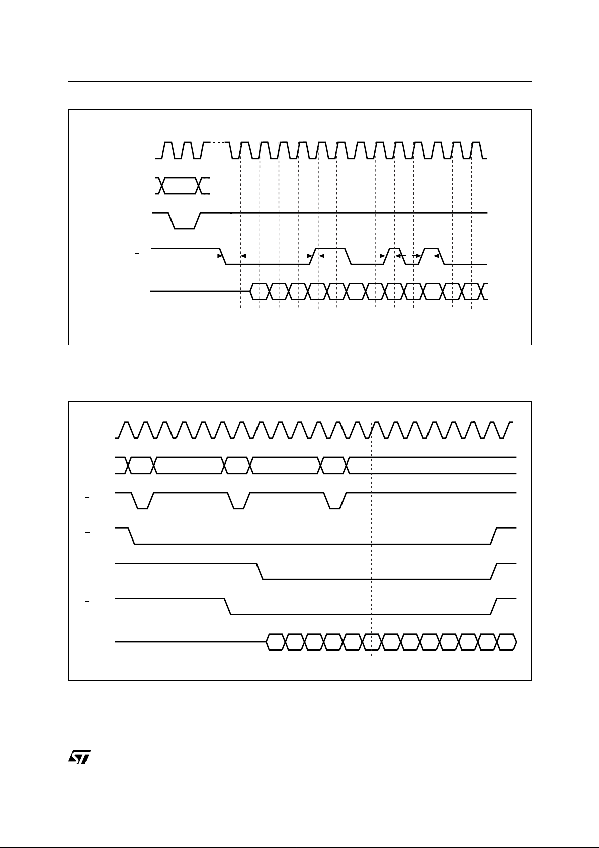
Figure 7. Sync h ronous Burst R ead Operation
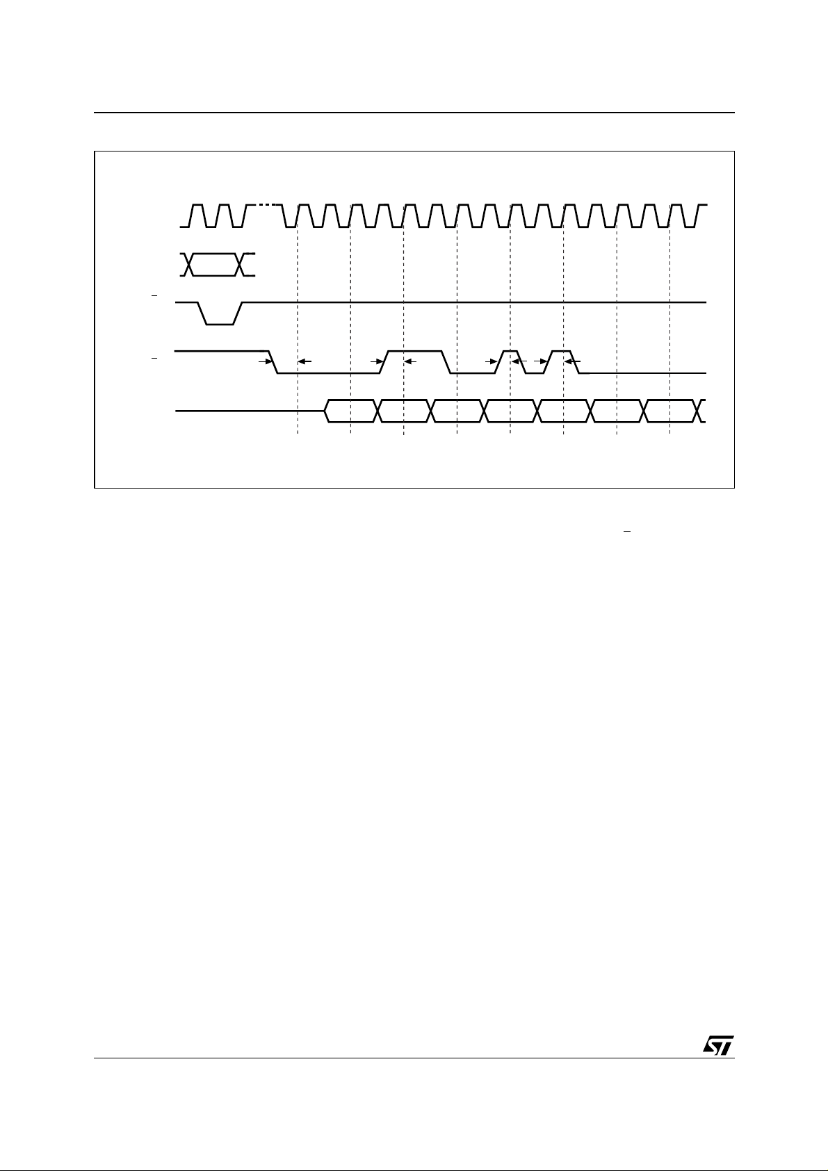
M58LV064A, M58LV064B
1
0
K
Address
Inputs
L
B
Data Inputs/
Outputs
Note: I n thi s exa mple t he Bur st Co nfigur at ion Regist er is set with M 2-M 0 = 001 (B urst Lengt h = 4 Wo rds or Doubl e Word s) , M6 = 1 (Valid
Clock Edge = Rising Clock Edge), M7 = 0 or 1 (Burst Type = Interleaved or Sequential), M9 = 0 (Y-Latency = 1), M14-M11 = 0011 (XLatency = 8) and M15 = 0 (Rea d Se l ect = Synchro nous Burst Read), other bi ts are don’t care.
Q1
X-1
X
tBLKH
Q1
X+1
Q2
tBHKH
tBHKH
Q5Q5Q5Q4Q3 Q7Q6 Q8Q8Q7
tBHKH
AI03454b
Figure 8. Example Sy nchronous Pipelin ed Burst Read Operati on
01234567891011121314
K
15
Address
Inputs
L
E
G
B
Data
Inputs/ Outputs
Note: I n thi s exa mple t he Bur st Co nfigur at ion Regist er is set with M 2-M 0 = 001 (B urst Lengt h = 4 Wo rds or Doubl e Word s) , M6 = 1 (Valid
Clock Edge = Rising Clock Edge), M7 = 0 or 1 (Burst Type = Interleaved or Sequential), M9 = 0 (Y-Latency = 1), M14-M11 = 0011 (XLatency = 8) and M15 = 0 (Rea d Se l ect = Synchro nous Burst Read), other bi ts are don’t care.
Q1 R1 S1
Q1
Q2 Q3 Q4 NV R1 R2 R3 R4 NV S1 S2
NV= Not Valid
S3
AI03455
19/65
Page 20
M58LV064A, M58LV064B
Figure 9. Example Burst Address Advance and Burst Abort operations
1
0
K
Address
Inputs
L
B
Data Inputs/
Outputs
Note: 1. In this ex amp le the B ur st Co nfigur ati on Reg ister is s et wit h M2- M0 = 01 0 (Bur st Le ngth = 8 Wo rds), M6 = 1 (Val id Cl ock Edg e =
Rising Clock Edge), M 7 = 0 or 1 (B urst Type = In terleaved or Sequenti al ), M9 = 1 (Y-Latency = 2), M14-M1 1 = 0011 (X- Latency =
8) and M15 = 0 (Read Select = Sy nchronous Burst Read), other bits are don’t care.
2. When the system clock f requency is between 33MHz and 50MHz and the Y la tency is set to 2, values of B
cycles, starting from t he first read are not conside red.
Q1
X-2
tBLKH
Q1 Q2
X
X+2
tBHKH
X+6X+4 X+12X+10X+8
tBHKH
Q3 Q4 Q4
tBHKH
Q4Q3
AI03457b
sampled on odd clock
20/65
Page 21

M58LV064A, M58LV064B
Burst Configuration Register
The Burst Configuration Register is used to configure the type of bus access that the memory will
perform.
The Burst Configuration Register is set through
the Command Interface and will retain its information until it is re-configured, the device is reset, or
the device goes into Reset/Power-Down mode.
The Burst Configuration Register bits are described in Table 5. They s pecify the selection of
the burst length, burst type, burst X and Y latencies and the Read operation.
Read Select Bit (M15). The Read Select bit,
M15, is used to switch between asynchronous and
synchronous Bus Read operations. When the
Read Select bit is set to ’1’, Bus Read operations
are asynchronous; when the Read Select but is
set to ’0’, Bus Read operations are synchronous.
On reset or power-up the Read Sel ect bit is set
to’1’ for asynchronous accesses.
X-Latency Bits (M14-M11). The X-Latency bits
are used during Synchronous Bus Read operations to set the number of clock cycles between
the address being latched and the first data becoming available. For correct operation the X-Latency bits can only assume the values in Table 5,
Burst Configuration Register. The X-Laten cy bits
should also be sele cted in con junction with Tab le
8, Burst Performance to ensure valid settings.
Y-Latency Bit (M9). The Y-Latency bit is used
during Synchronous Bus Read operations to set
the number of clock cycles between consecutive
reads. The Y-Latency value depends on both the
X-Latency value and the setting in M9.
When the Y-Latency is 1 the data changes each
clock cycle; when the Y-Latency is 2 the data
changes every seco nd clock cycle. See Tab le 5,
Burst Configuration Register and Table 8, Burst
Performance, for valid combi nations of the Y-Latency, the X-Latency and the Clock frequency.
Valid Data Ready Bit (M8). The Valid Data
Ready bit controls the timing of the Valid Data
Ready output pin, R. When the Valid Data Ready
bit is ’0’ the Valid Data Ready output pin is driven
Low for the active clock edge when invalid data is
output on the bus. When the Valid Data Ready bit
is ’1’ the Valid Data Ready output pin is driven Low
one clock cycle prior to invalid data being output
on the bus.
Burst Type Bit (M7 ). The Burst Type bit is used
to configure the sequence of addresses read as
sequential or interleaved. When the Burst Type bit
is ’0’ the memory outputs from interleaved addresses; when the Burst Type bit is ’1’ the memory
outputs from sequential ad dresses. See Tables 6
and 7, Burst Type Definition, for t he sequence of
addresses output from a give n starting a ddress in
each mode.
Valid Clock Edge Bit (M6). The Valid Clock Edge
bit, M6, is used to configure the active edge of the
Clock, K, during Synchronous Burst Read operations. When the Valid Clock Edge bit is ’0’ the falling edge of the Clock is the active edge; when the
Valid Clock Edge bit is ’1’ the risi ng edge of the
Clock is active.
Latch Enable Bit (M3). The Latch Enable bit is
used to select between Asynchronous Random
Read and Asynchronous La tch Enable Controlled
Read. When the Latch Enable bit is set to ‘0’ Random read is selected; when it is set to ‘1’ Latch Enable Controlled Read is selected. To enable these
Asynchronous Read configuration s M15 must be
set to ‘1’.
Burst Length Bit (M2-M0). The Burst Length bits
set the maximum number of Words or DoubleWords that can be ou tput during a Synchronous
Burst Read operation before the address wraps.
Table 5, Burst Configuration Register gives the
valid combinations of the Burst Length bits that the
memory accepts; Tables 6 and 7, Burst Type Definition, give the sequence of addresses output
from a given starting address for each length.
M10, M5 an d M4 are reserved for future use.
21/65
Page 22

M58LV064A, M58LV064B
Table 5. Burst Configuration Register
Address
Bit
17 M15
Mnemonic Bit Name
Read
Select
Reset
Value
1
Value Description
0 Synchronous Burst Read x16 or x32
1 Asynchronous Bus Read x16 or x32
0010
0011 X-Latency = 8 x16 or x32
0100 X-Latency = 9 x16 or x32
X-Latency = 7, use only with Continuous Burst
Length
Valid Bus
Width
x16 or x32
16
to
13
11 M9
10 M8
to
M14-M11 X-Latency XXXX
Y-Latency
Valid Data
Ready
9 M7 Burst Type X
8M6
5M3
4
M2-M0
2
Valid Clock
Edge
Latch
Enable
Burst
Length
0101
0110
1001 X-Latency = 12 x16 only
1010 X-Latency = 13 x16 only
1011
1101 X-Latency = 15 x16 or x32
Others Reserved, Do Not Use.
X
X
X
0
XXX
X-Latency = 10, use only with Continuous Burst
Length
X-Latency = 11, use only with Continuous Burst
Length
X-Latency = 13, use only with Continuous Burst
Length
When X-Latency < 13, Y-Latency = 1
0
When M14-M11 = 1011 or 1101, Y-Latency = 2
When X-Latency ≤15 but M14-M11≠1011 or
1
1101, Y-Latency = 2,
When M14-M11=1011 or 1101 DO NOT USE.
0 R valid Low during valid Clock edge x16 or x32
1 R valid Low one cycle before valid Clock edge x16 or x32
0 Interleaved x16 or x32
1 Sequential x16 or x32
0 Falling Clock edge x16 or x32
1 Rising Clock edge x16 or x32
0 Random Read x16 or x32
1 Latch Enable Controlled Read x16 or x32
100 1 Word or Double-Word x16 or x32
101 2 Words or Double-Words x16 or x32
001 4 Words or Double-Words x16 or x32
010 8 Words x16 only
111 Continuous x16 or x32
x16 only
x16 only
x16 or x32
x16 or x32
x16 or x32
22/65
Others Reserved, Do Not Use.
Page 23

Table 6. Burst Type Definition (x16 Bus Width)
Starting Addres s
Burst Length
(binary)
A3 A2 A1
Sequential
(decimal)
M58LV064A, M58LV064B
Interleaved
(decimal)
2
4
8
Continuous A A, A+1, A+2... Not Valid
Note: X = 0 or 1.
XX0 0, 1 0, 1
XX1 1, 0 1, 0
X00 0, 1, 2, 3 0, 1, 2, 3
X01 1, 2, 3, 0 1, 0, 3, 2
X10 2, 3, 0, 1 2, 3, 0, 1
X11 3, 0, 1, 2 3, 2, 1, 0
000 0, 1, 2, 3, 4, 5, 6, 7 0, 1, 2, 3, 4, 5, 6, 7
001 1, 2, 3, 4, 5, 6, 7, 0 1, 0, 3, 2, 5, 4, 7, 6
010 2, 3, 4, 5, 6, 7, 0, 1 2, 3, 0, 1, 6, 7, 4, 5
011 3, 4, 5, 6, 7, 0, 1, 2 3, 2, 1, 0, 7, 6, 5, 4
100 4, 5, 6, 7, 0, 1, 2, 3 4, 5, 6, 7, 0, 1, 2, 3
101 5, 6, 7, 0, 1, 2, 3, 4 5, 4, 7, 6, 1, 0, 3, 2
110 6, 7, 0, 1, 2, 3, 4, 5 6, 7, 4, 5, 2, 3, 0, 1
111 7, 0, 1, 2, 3, 4, 5, 6 7, 6, 5, 4, 3, 2, 1, 0
Table 7. Burst Type Definition (x32 Bus Width)
Burst Length
Starting Addres s
(binary)
A3 A2
Sequential
(decimal)
Interleaved
(decimal)
2
X0 0, 1 0, 1
X1 1, 0 1, 0
00 0, 1, 2, 3 0, 1, 2, 3
01 1, 2, 3, 0 1, 0, 3, 2
4
10 2, 3, 0, 1 2, 3, 0, 1
11 3, 0, 1, 2 3, 2, 1, 0
8 Not Valid
Continuous A A, A+1, A+2... Not Valid
Note: X = 0 or 1.
23/65
Page 24

M58LV064A, M58LV064B
Table 8. Burst Performance
X-Latency Y-Latency Bus Width Clock Frequency Mode
7
8
9
7
8
9
10
11
12
13
10
11
12
13
13
15 continuous, length
1
x16, x32 ≤ 33 MHz
2
1
x16 only ≤ 50 MHz
2
2(M9=0) x16, x32 ≤ 66 MHz
continuous only
continuous, length
continuous only
continuous, length
continuous only
continuous, length
continuous only
continuous, length
continuous only
24/65
Page 25

COMMAND INTERFACE
All Bus Write operations t o the me mory are in terpreted by the Command Interface. Commands
consist of one or more sequential Bus Write operations. The Commands are summarized in Table
9, Commands. Refer to Table 9 in conjunction with
the text descriptions below.
After power-up or a Reset operation the memory
enters Read mode.
Synchronous Read operations and Latch Controlled Bus Read operations can only be used to
read the memory array. The Electr onic Sign ature,
CFI or Sta tus Register w ill be read in async hronous mode regardless of the Burst Control Register settings. Once the memory returns to Read
Memory Array mode the bus will resume the setting in the Burst Configuration Register automatically.
Read Memory A rray Command. The Read Memory Array command returns the memory to Read
mode. One Bus Write cycle is required to issue the
Read Memory Array command and return the
memory to Read mode. Once the command is issued the memory remains in Read m ode until another command is issued. From Rea d mode B us
Read commands will access the memory array.
While the Program/Erase Controller is executing a
Program, Erase, Block Protect or Blocks Unprotect operation the memory will not accept the Read
Memory Array command until the operation completes.
Read Electr onic S ignature Co m mand. The Read
Electronic Signature command is used to read the
Manufacturer Code, the Device Code and the
Block Protection Status. One Bus Write cycle is required to issue the Read Electronic Signature
command. Once the command is issued subsequent Bus Read operations read the Manufacturer
Code, the Device Code or the Block Protection
Status until another command is issued; see Table
10, Read Electronic Signature.
Read Query Command. The Read Query Command is used to read data from the Common Flash
Interface (CFI) Memory Area . One Bus Write cycle
is required to issue the Read Query Command.
Once the command is issued subsequent Bus
Read operations read from the Common Flash Interface Memory Area. See Appendix B, Tables 29,
30, 31, 32, 33 and 34 for details on the information
contained in the Common Flash Interface (CFI)
memory area.
Note that the addresses for the Common Flash Interface Memory Area are A1-A22 for
theM58LV064A an d A2-A22 for th e M58LV064B,
regardless of the Bus Width selected.
Read Stat us Register Co mm an d . The Read Status Register command is us ed to read the Status
M58LV064A, M58LV064B
Register. One Bus Write cycle is required to issue
the Read Status Register command. Once the
command is issued subsequent Bus Read operations read the Status Register until another command is issued.
The Status Register information is present on the
output data bus (DQ1-DQ 7) when both Chip Enable and Output Enable are low, V
See the section on the Status Reg ister and Table
12 for details on the definitions of the Status Register bits
Clear Status Register Command. The Clear Status Register command can be used to reset bits 1,
3, 4 and 5 in the Status Register to ‘0’. One Bus
Write is required to issue the Clear Status Register
command.
The bits in the Status Register are sticky an d do
not automatically return to ‘0’ when a new Write to
Buffer and Program, Erase, Block Protect or Block
Unprotect command is issued. If any error occurs
then it is essential to clear any error bits in the Status Register by issuing the Clear Status Register
command before attempting a new Program,
Erase or Resume command.
Block Erase Command. The Block Erase command can be used to e rase a block. It sets all of
the bits in the block to ‘1’. All previous data in the
block is lost. If the block is protected then the
Erase operation will abort, the data in the block will
not be changed and the Status Register will output
the error.
Two Bus Write operations are required to issue the
command; the second Bus Write cycle latches the
block address in the internal state machine and
starts the Program/Erase Controller. Once the
command is issued subsequent Bus Read operations read the Status Register. See the section on
the Status Register for details on the definitions of
the Status Register bits.
During the Erase operation the memory will only
accept the Read Status Register command and
the Program/Erase Su spend command. All ot her
commands will be ignored. Typical Erase times
are given in Table 11.
See Appendix C, Figure 27, Block Erase Flowchart and Pseudo Code, for a suggested flowchart
on using the Block Erase command.
Write to Buffer and Program Comm and. The
Write to Buffer and Program command is used to
program the memory array.
Up to 4 pages of 4 Words (or 2 Double Words) can
be loaded into the Write Buffer and program med
into the memory. The 4 pages are selected by addresses A3 and A4; each page has the sam e A 3A22.
.
IL
25/65
Page 26

M58LV064A, M58LV064B
Four successive steps are required to issue the
command.
1. One Bus Write operation is required to set up
the Write to Buffer and Program Comm and. Issue the set up command with the selected
memory Block Address where the program operation should occur (any address in the block
where the values will be programmed can be
used). Any Bus Read operations will start to output the Status Register after the 1st cycle.
2. Use one Bus Write operat ion to write the same
block address along with the value N on the
Data Inputs/Output, where N+1 is the number of
Words (x16 Bus Wi dth) or Double Words (x32
Bus Width) to be programmed.
3. Use N+1 Bus Write operations to load the address and data for each Word or Double Word
into the Write Buffer. See the constraints on the
address combinations listed below. The addresses must have the same A5-A22.
4. Finally, use one Bus Write operation to issue the
final cycle to confirm the command and start the
Program operation.
Invalid address combinations or failing to follow
the correct sequence of Bus Write cycles will set
an error in the Status Register and abort the operation without affecting the data in the mem ory array. The Status Register should be cleared before
re-issuing the command.
The minimum buffer size f or a program operation
is a 4 Wo rd (or 2 Doubl e Word) page. I nside the
page the 4 Words are selected by addresses A 2
and A1. Any attempt to program a s ingle word (or
Double Word) inside the page of a previously
erased block will result in the programming of the
Word, however all other Words inside the page will
be set to FFFFh.
For any page, only one Write to Buffer and P rogram Command can be issued inside a previously
erased block. Any further Program operations on
that page must be preceded by an Erase operation
on the respective block.
If the block being program m ed i s prote cted an error will be set in the Status Register and the operation will abort without affecting the data in the
memory array. The block must be unprotected using the Blocks Unprotect command or by using the
Blocks Temporary Unprotect feature of the Reset/
Power-Down pin, RP
.
See Appendix C, Figure 25, Write t o Buffer and
Program Flowchart and Pseudo Code, for a suggested flowchart on using the W rite to B uffer and
Program command.
Program/Erase Suspend Command. The Program/Erase Su spend command is used to pause a
Write to Buffer and Program or Erase operation.
The command will on ly be acc ep t ed du ring a Program or an Erase operation. It can be issued at
any time during an Erase operation but will only be
accepted during a Write to Buffer and Program
command if the Program/Erase Controller is running.
One Bus Write cycle is required to i ssue the P rogram/Erase Suspend command and pause the
Program/Erase Controller. Once the command is
issued it is necessary to poll the Program/Erase
Controller Status bit (bit 7) to find out when the
Program/Erase Controller has paused; no other
commands will be accepted until the Program/
Erase Controller has paused. After the Program/
Erase Controller has paused, the memory will continue to output the Status Register until another
command is issued.
During the polling period between issuing the Program/Erase Suspend command and the Program/
Erase Controller pausing it is possible for the operation to complete. Once the Program/Erase
Controller Status bit (bit 7) i ndicates t hat the Program/Erase Controller is no longer active, the Program Suspend Status bit (bit 2) or the Erase
Suspend Status bit (bit 6) can be used to determine if the operation has completed or is suspended. For timing on the delay between issuing the
Program/Erase Suspend command and the Program/Erase Controller pausing see Table 11.
During Program/Erase Suspend the Read Memory Array, Read Status Register, Read Elect ronic
Signature, Read Query and Program/Erase Resume commands will be accepted by the Command Interface. Additionally, if the suspended
operation was Erase then the W rite to B uffer and
Program, and the Program Suspend commands
will also be ac cepted. W hen a program o peration
is completed inside a Block Erase Suspend the
Read Memory Array command m ust be issued to
reset the device in Read mode, then the Erase Resume command can be issued to complete the
whole sequence. Only the blocks not being erased
may be read or programmed correctly.
See Appendix C, Figure 26 , Program Suspend &
Resume Flowchart and Pseudo Code, and Figure
28, Erase Suspend & Resume Flowchart and
Pseudo Code, for suggested flowcharts on using
the Program/Erase Suspend command .
Program / Erase Resum e Command. The Program/Erase Resume command can be used to restart the Program/Erase Controller after a
Program/Erase Suspend operat ion h as paused it.
One Bus Write cycle is required to i ssue the P rogram/Erase Resume command. Once the command is issued subsequ ent Bus Read operations
read the Status Register.
26/65
Page 27

M58LV064A, M58LV064B
Set Burst Configuration Register Command.
The Set Burst Configuration Register command is
used to write a new value t o the Burst Conf iguration Control Register which defines the burst
length, type, X and Y latencies, Synchronous/
Asynchronous Read mode and the valid Clock
edge configuration.
Two Bus Writ e cycle s are required to issue th e Se t
Burst Configuration Register command. Once the
command is issued the memory returns to Read
mode as if a Read Mem ory Array command had
been issued.
The value for the Burst Configuration Register is
always presented on A2-A17, regardless of the
bus width that is selected. M0 is on A2, M1 on A3,
etc.; the other address bits are ignored.
Block Protect Command. The Block Protect
command is used to protec t a block and prevent
Program or Erase operations from changing the
data in it. Two Bus Write cycles are required to issue the Block Protect command; the second Bus
Write cycle latches the block address in the internal state machine and sta rts the Program/Erase
Controller. Once the command is issued subsequent Bus Read operations read the Status Register. See the section on the Status Register for
details on the definitions of the Status Register
bits.
During the Block Protect operation the memory will
only accept the Read Status Re gister command.
All other commands will be ignored. Typical Block
Protection times are given in Table 11.
The Block Protection bits are non-volatile, once
set they remain set through reset and powerdown/power-up. They ar e cleared by a Blocks Unprotect command or temporary disabled by raising
the Reset/Power-Down pin to V
and holding it at
HH
that level throughout a Block Erase or Write to
Buffer and Program command.
Blocks Unprotect Command. The Blocks Unprotect command is used to unprotect all of the
blocks. Two Bus Write cycl es are required to issue
the Blocks Unprotect command ; the second Bus
Write cycle starts the Program/Erase Controller.
Once the command is issued subsequent Bus
Read operations read the Status Register. See the
section on the Stat us Register for details on the
definitions of the Status Register bits.
During the Block Unprotect operation the memory
will only accept the Read Status Register command. All other commands will be ignored. Typical
Block Protection times are given in Table 11.
27/65
Page 28

M58LV064A, M58LV064B
Table 9. Commands
Bus Write Operations
Command
Cycles
Read Memory Array 1 X FFh
Read Electronic Signature 1 X 90h
Read Query 1 X 98h
Read Status Register 1 X 70h
Clear Status Register 1 X 50h
Block Erase 2 X 20h BA D0h
Write to Buffer and Program 4 + N BA E8h BA N PA PD X D0h
Program/Erase Suspend 1 X B0h
Program/Erase Resume 1 X D0h
Set Burst Configuration Register 2 BCR 60h BCR 03h
Block Protect 2 BA 60h BA 01h
Blocks Unprotect 2 X 60h X D0h
Note: X Don’t Care; PA P rogram Address; P D Program Data ; BA Any address in the Block; N+1 Number of Addresse s to Program;
BCR Burst Configura t io n Register value.
Table 10. Read Electronic Signature
Code
Manufacturer Code
Device Code
Block Protection Status
Note: 1. SBA is the S t art Base Address of each block.
2. DQ31-DQ16 are av ai l able in the M58LV064B only.
3. x32 Bus Width is avai l able in the M58LV064B onl y.
4. The address is presented on A22-A2 in x32 mode, and on A22-A1 in x16 mo de.
Bus Width
x16
x32 00000020h
x16
x32 00000014h (M58LV064B)
x16
x32
1st 2nd Subsequent Final
Addr Data Addr Data Addr Data Addr Data
(3)
Address
(4)
Data (DQ31-DQ0)
(2)
0020h
000000h
0015h (M58LV064A)
000001h
0014h (M58LV064B)
0000h (Block Unprotected)
SBA
(1)
+02h
0001h (Block Protected)
00000000h (Block Unprotected)
00000001h (Block Protected)
28/65
Page 29

M58LV064A, M58LV064B
Table 11. Program, Erase Times and Progr am Eras e Endur ance Cycles
M58LV064A/B
Parameters
Min Typ
Typical after
100k W/E Cycles
Max
Block (1Mb) Erase 0.75 0.75 5 s
Chip Program 54 54 s
Program Write Buffer 192 192 µs
Program Suspend Latency Time 3 10 µs
Erase Suspend Latency Time 10 30 µs
Block Protect Time 192 µs
Blocks Unprotect Time 0.75 s
Program/Erase Cycles (per Block) 100,000 cycles
Data Retention 20 years
Note: (TA = 0 to 70°C; VDD = 2.7V to 3.6V; V
DDQ
=1.8V)
Unit
29/65
Page 30

M58LV064A, M58LV064B
STATUS REGISTER
The Status Register provides information on t he
current or previous Program, Erase, Block Protect
or Blocks Unprotect operation. The various bits in
the Status Register convey information and errors
on the operation. They are output on DQ7-DQ0.
To read the Status Register the Read Status Register command can be issued. The Status Register
is automatically read after Program, Erase, Block
Protect, Blocks Unprotect and Program/Erase Resume commands. The Status Register can be
read from any address.
The Status Register can only be read using Asynchronous Bus Read operations. Once the memory
returns to Read Memory Array mode the bus will
resume the setting in the Burst Configuration Register automatically.
The contents of the Status Register can be updated during an Erase or Program operat ion by toggling the Output Enable pin or by dis-activating
(Chip Enable, V
able and Output Enable, V
Status Register bits 5, 4, 3 and 1 are associated
with various error conditions and can only be reset
with the Clear Status Register command. The Status Register bits are summarized in Table 12, Status Register Bits. Refer to Table 12 in conjunction
with the following text descriptions.
Program/Erase Controller Status (Bit 7). The Progra m/Erase Controller Status bit indicates whether
the Program/Erase Controller is active or inactive.
When the Program/Erase Controller Status bit is
Low, V
, the Program/Erase Controller is active
OL
and all other Status Register bits are High Impedance; when the bit is High, V
Erase Controller is inactive.
The Program/Erase Controller Status is Low immediately after a Program/Erase Suspend command is issued until the Program/Erase Controller
pauses. After the Program/Erase Controller pauses the bit is High.
During Program, Erase, Block Protect and Blocks
Unprotect operations the Program/Erase Controller Status bit can be polled to find the end of the
operation. The other bits in the Status Register
should not be tested until the Program/Erase Controller completes the operation and the bit is High.
After the Program/Erase Cont roller completes its
operation the Erase S tatus, Program Status and
Block Protection Status bits should be tested for
errors.
Erase Suspend Status (Bit 6). The Erase Suspend Status bit indicates that an Erase o peration
has been suspended and is waiting to be resumed. The Erase Suspend Status should only be
considered valid when the Program/Erase Controller Status bit is High (Program/Erase Controller
) and then reactivating (Chip En-
IH
) the device.
IL
, the Program/
OH
inactive); after a Program/Erase Suspend command is issued the memory may still complete the
operation rather than entering the Suspend mode.
When the Erase Suspend Statu s bit is Low, V
OL
the Program/Erase Controller is active or has completed its operation; when the bit is High, V
OH
, a
Program/Erase Suspend com mand has been issued and the memory is waiting for a Program/
Erase Resume command.
When a Program/Erase Re sume command is issued the Erase Suspend Status bit returns Low.
Erase Status (Bit 5). The Erase Status bit can be
used to identify if the memory has failed to verify
that the block has erased correctly or that all
blocks have been unprotected successfully. The
Erase Status bit should be read once the Program/
Erase Controller Status bit is High (Program/Erase
Controller inactive).
When the Erase St atu s bit i s Low, V
, the mem-
OL
ory has successfully verified that the block has
erased correctly or all blocks have been unprotected successfully. When the Erase Status bit is
High, V
, the erase operation has failed. De-
OH
pending on the cause of the failure othe r Status
Register bits may also be set to High, V
■ If only the Erase Status bit (bit 5) is set High,
V
, then the Program/Erase Controller has
OH
OH
.
applied the maximum number of pulses to the
block and still failed to verify that the block has
erased correctly or that all the blocks have been
unprotected successfully.
■ If the failure is due to an erase or blocks
unprotect with V
(bit 3) is also set High, V
■ If the failure is due to an erase on a protected
low, VOL, then VPP Status bit
PP
OH
.
block then Block Protection Status bit (bit 1) is
also set High, V
■ If the failure is due to a program or erase
OH
.
incorrect command sequence then Program
Status bit (bit 4) is also set High, V
OH
.
Once set High, the Erase Status bit can only be reset Low by a Clear Status Register command or a
hardware reset. If set High it should be reset before a new Program or Erase command is issued,
otherwise the new command will appear to fail.
Program Status (Bit 4). The Program Status bit
is used to identify a Program or Block P rotect f ailure. The Program S tatus bit shoul d be read once
the Program/Erase Controller Status bit is High
(Program/Erase Controller inactive).
When the Program Status bit is Low, V
OL
, the
memory has successfully verified that the Write
Buffer has programmed correc tly or the block is
protected. When the Program Status bit is High,
V
, the program or block protect operation has
OH
,
30/65
Page 31

M58LV064A, M58LV064B
failed. Depending on the cause of the failure other
Status Register bits may also be set to High, V
■ If only the Program Status bit (bit 4) is set High,
V
, then the Program/Erase Controller has
OH
OH
applied the maximum number of pulses to the
byte and still failed to verify that the Write Buffer
has programmed correctly or that the Block is
protected.
■ If the failure is due to a program or bl ock protect
with V
also set High, V
■ If the failure is due to a program on a protected
low, VOL, then VPP Status bit (bit 3) is
PP
OH
.
block then Block Protection Status bit (bit 1) is
also set High, V
■ If the failure is due to a program or erase
OH
.
incorrect command sequence then Erase
Status bit (bit 5) is also set High, V
OH
.
Once set High, the Program Status bit can only be
reset Low by a Clear Status Register command or
a hardware reset. If set High it should be reset before a new Program or Erase command is issued,
otherwise the new command will appear to fail.
Status (Bit 3). The VPP Status bit can be
V
PP
used to identify if a Program, Erase, Block Protection or Block Unprotection operation has been attempted when V
is Low, VIL. The VPP pin is only
PP
sampled at the beginning of a Program or Erase
operation.
When the V
Status bit is Low, VOL, no Program,
PP
Erase, Block Protection or Block Unprotection operations have been attempted with V
Low, VIL,
PP
since the last Clear Status Register command, or
hardware reset. When the V
V
, a Program, Erase, Block Protection or Block
OH
Status bit is High,
PP
Unprotection operation has been a ttempted with
V
Low, VIL.
PP
Once set High, the V
Status bit can only be reset
PP
by a Clear Status Register command or a hardware reset. If set High it should be reset befo re a
new Program, Erase, Block Protection or Block
Unprotection command is issued, otherwise the
new command will appear to fail.
.
Program Suspend Status (Bit 2). The Program
Suspend Status bit indicates that a Program operation has been suspended and is waiting to be resumed. The Program Suspend Status should only
be considered valid when the Program/Erase
Controller Status bit is High (Program/Erase Controller inactive); after a Program/Erase Suspend
command is issued the memory may still complete
the operation rather than entering the Suspend
mode.
When the Program Suspend Status bit is Low,
V
, the Program/Erase Controller is active or has
OL
completed its operation; when the bit is High, V
a Program/Erase Suspend command has been issued and the memory is waiting for a Program/
Erase Resume command.
When a Program/Erase Re sume command is issued the Program Suspend Status bit returns Low.
Block Protection Status (Bit 1). The Block Protection Status bit can be used to identify if a Program or Erase operation has tried to modify the
contents of a protected block.
When the Block Protection Status bit is Low, V
no Program or Erase operations have been attempted to protected blocks since the last Clear
Status Register command or hardware reset;
when the Block Protection Status bit is High, V
a Program (Program Status bit 4 set High) or
Erase (Erase Status bit 5 set High) operation has
been attempted on a protected block.
Once set High, the Block Protection Status bit can
only be reset Low by a Clear Status Register command or a hardware reset. If set High it should be
reset before a new Program or Erase command is
issued, otherwise the new command will appear to
fail.
Reserved (Bit 0). Bit 0 of the Status Register is
reserved. Its value should be masked.
OH
OL
OH
,
,
,
31/65
Page 32

M58LV064A, M58LV064B
Table 12. Status Register Bits
Operation Bit 7 Bit 6 Bit 5 Bit 4 Bit 3 Bit 2 Bit 1 RB
Program/Erase Controller Active ‘0’ Hi-Z
Write Buffer not ready ‘0’ Hi-Z
’1’
’1’
(1)
X
X
X
X
X
X
X
‘0’ ‘0’ ‘0’ ‘0’ ‘0’ Hi-Z
(1)
‘0’ ‘0’ ‘0’ ‘1’ ‘0’ Hi-Z
(1)
‘0’ ‘0’ ‘0’ ‘0’ ‘0’ Hi-Z
(1)
‘1’ ‘1’ ‘0’ ‘0’ ‘0’ Hi-Z
(1)
‘0’ ‘1’ ‘1’ ‘0’ ‘0’ Hi-Z
(1)
‘0’ ‘1’ ‘0’ ‘0’ ‘1’ Hi-Z
(1)
‘0’ ‘1’ ‘0’ ‘0’ ‘0’ Hi-Z
Write Buffer ready ‘1’
Program suspended ‘1’
Program/Block Protect completed successfully ‘1’
Program/Block Protect failure due to incorrect command
sequence
Program/Block Protect failure due to V
PP
Error
Program failure due to Block Protection ‘1’
Program/Block Protect failure due cell failure or unerased cell ‘1’
V
V
Erase suspended ‘1’ ‘1’ ‘0’ ‘0’ ‘0’ ‘0’ ‘0’ Hi-Z
Erase/Blocks Unprotect completed successfully ‘1’ ‘0’ ‘0’ ‘0’ ‘0’ ‘0’ ‘0’ Hi-Z
Erase/Blocks Unprotect failure due to incorrect command
sequence
Erase/Block Unprotect failure due to V
PP
Error
‘1’
‘1’ ‘1’ ‘0’ ‘0’ ‘0’ Hi-Z
X
’1’ ‘0’ ‘1’ ‘0’ ‘1’ ‘0’ ‘0’ Hi-Z
Erase failure due to Block Protection ‘1’ ‘0’ ‘1’ ‘0’ ‘0’ ‘0’ ‘1’ Hi-Z
Erase/Blocks Unprotect failure due to failed cell(s) in block ‘1’ ‘0’ ‘1’ ‘0’ ‘0’ ‘0’ ‘0’ Hi-Z
Note: 1. For Program operat i ons during Er ase Suspend Bit 6 is ‘1’, otherwise Bit 6 is ‘0 ’ .
OL
OL
32/65
Page 33

MAXIMUM RATIN G
Stressing the device above the ratings listed in Table 13, Absolute Maximum Ratings, may cause
permanent damage to the device. These are
stress ratings only and operation of the dev ice at
these or any other conditions above those indicat-
not implied. Exposure to Absol ute Maxim um Rating conditions for extended periods may affect device reliability. Refer also to the
STMicroelectronics SURE Program and oth er relevant quality documents.
ed in the Operating sections of this specification is
Table 13. Absolute Maximum Ratings
Symbol Parameter
T
BIAS
T
STG
T
LEAD
V
IO
, V
V
DD
DDQ
V
HH
Note: 1. Cumulative time at a hi gh voltage level of 10V should not exce ed 80 hours on RP pi n.
Temperature Under Bias –40 125 °C
Storage Temperature –55 150 °C
Maximum TLEAD Temperature during soldering t.b.a. °C
Input or Output Voltage –0.6
Supply Voltage –0.6 5.0 V
RP Hardware Block Unprotect Voltage –0.6
M58LV064A, M58LV064B
Value
Min Max
V
+0.6
DDQ
(1)
10
Unit
V
V
33/65
Page 34

M58LV064A, M58LV064B
DC AND AC PARAMETERS
This section summarizes the operat ing and measurement conditions, and the DC and AC characteristics of the device. The parameters in the DC
and AC characteristics Tables that follow, are derived from tests performed under the Measure-
Table 14. Operating and AC Measurement Conditions
Parameter
Supply Voltage (V
Input/Output Supply Voltage (V
Ambient Temperature (T
Load Capacitance (C
Clock Rise and Fall Times 3 ns
Input Rise and Fall Times 4 ns
Input Pulses Voltages
Input and Output Timing Ref. Voltages
) M58LV064
DD
A
)
L
)
DDQ
)
Grade 1 0 70 °C
Grade 6 –40 85 °C
ment Conditions summarized in Table 14,
Operating and AC Measurem ent Conditions. Designers should check that the operating conditions
in their circuit match the measurement conditions
when relying on the quoted parameters.
M58LV064
Min Max
3.0 3.6 V
1.8
V
DD
30 pF
0 to V
DDQ
0.5 V
DDQ
Units
V
V
V
Figure 10. AC Measurement Input Output
Waveform
V
DDQ
0.5 V
0V
DDQ
AI00610
Figure 11. AC Measureme nt Load Circui t
1.3V
V
DDQ
V
DD
DEVICE
UNDER
TEST
0.1µF
0.1µF
CL includes JIG capacitance
Table 15. Capacitance
Symbol Parameter Test Condition Typ Max Unit
C
IN
C
OUT
Note: 1. TA = 25°C, f = 1 MHz
2. Sampled only, not 100% tested.
Input Capacitance
Output Capacitance
V
V
OUT
IN
= 0V
= 0V
68pF
812pF
1N914
3.3kΩ
C
L
DQ
AI03459
S
34/65
Page 35

M58LV064A, M58LV064B
Table 16. DC Characteristics
Symbol Parameter Test Condition Mi n Max Unit
I
LI
I
LO
I
DD
I
DDB
I
DD1
I
DD5
I
DD2
I
DD3
I
DD4
V
IL
V
IH
V
OL
V
OH
(1)
V
HH
I
HH
0V≤ V
Input Leakage Curren t
Output Leakage Current
Supply Current (Random Read)
Supply Current (Burst Read)
Supply Current (Standby)
Supply Current (Auto Low-Power)
Supply Current (Reset/Power-Down)
Supply Current (Program or Erase,
Set Block Protection, Unprotection)
Supply Current
(Erase/Program Suspend)
0V
E
= VIL, G = VIH, f
E
= VIL, G = VIH, f
= VIH, RP = V
E
E
Program or Erase operation in
≤ V
IN
DDQ
≤ V
OUT≤VDDQ
add
clock
= VIL, RP = V
RP
= V
IL
progress
= V
E
IH
= 6MHz
= 50MHz
IH
IH
±1 µA
±5 µA
30 mA
50 mA
40 µA
2mA
1 µA
50 mA
50 mA
Input Low Voltage –0.5 0.8 V
V
Input High Voltage
Output Low Voltage
Output High Voltage
RP Hardware Block Unprotect
Voltage
RP Hardware Block Unprotect
Current
I
= 100µA
OL
I
= –100µA V
OH
Block Erase in progress,
Write to Buffer and Program
= V
RP
HH
–0.8 V
DDQ
–0.1
DDQ
8.5 9.5 V
+ 0.5
DDQ
0.1 V
1 µA
V
V
V
Note: 1. Biasing RP pin to VHH is allowed for a maximum cum ulative peri od of 80 hours .
VDD Supply Voltage (Erase and
LKO
Program lockout)
2.2 V
35/65
Page 36

M58LV064A, M58LV064B
Figure 12. Asynchronous Bus Read AC Waveforms
tAVAV
A1-A22
VALID
tELQV
tELQX
E
tGLQV
tGLQX
G
tAVQV
DQ0-DQx
Note: Asynchronous Read ( M15 = 1), Random Read (M3 = 0)
OUTPUT
Table 17. Asynchronous Bus Read AC Characteristics.
Symbol Parameter Test Condition
t
AVAV
t
AVQV
t
ELQX
t
ELQV
t
GLQX
t
GLQV
t
EHQX
t
GHQX
t
AXQX
t
EHQZ
t
GHQZ
Address Valid to Address Valid
Address Valid to Output Valid
Chip Enable Low to Output Transition
Chip Enable Low to Output Valid
Output Enable Low to Output Transition
Output Enable Low to Output Valid
Chip Enable High to Output Transition
Output Enable High to Output Transition
Address Transition to Output Transition
Chip Enable High to Output Hi-Z
Output Enable High to Output Hi-Z
E
= VIL, G = V
E
= VIL, G = V
G
= V
G
= V
E
= V
E
= V
G
= V
E
= V
E
= VIL, G = V
G
= V
E
= V
IL
IL
IL
IL
IL
IL
IL
IL
IL
IL
IL
tAXQX
tEHQZ
tEHQX
tGHQZ
tGHQX
AI03250b
M58LV064
Unit
150
Min 150 ns
Max 150 ns
Min 0 ns
Max 150 ns
Min 0 ns
Max 30 ns
Min 0 ns
Min 0 ns
Min 0 ns
Max 10 ns
Max 10 ns
36/65
Page 37

Figure 13. Asynchronous Latch Controlled Bus Read AC Waveforms
M58LV064A, M58LV064B
A1-A22
tAVLL
L
E
G
DQ0-DQx
Note: Asynchronous Read (M15 = 1), Latch Enable Controlled (M3 = 1)
tAVLH
VALID
tELLL
tLLLH
tELLH
tGLQV
tGLQX
tLLQX
tLLQV
tLHAX
tEHLXtLHLL
tEHQZ
tEHQX
tGHQX
OUTPUT
Table 18. Asynchronous Latch Controlled Bu s Read AC Charac teris tics
Symbol Parameter Test Condition
t
AVLL
t
AVLH
t
LHLL
t
LLLH
t
ELLL
t
ELLH
t
LLQX
t
LLQV
t
LHAX
t
GLQX
t
GLQV
t
EHLX
Note: F or other tim i ngs see Tabl e 17, Asynchronous B us Read Characteristi cs.
Address Valid to Latch Enable Low
Address Valid to Latch Enable High
Latch Enable High to Latch Enable Low Min 10 ns
Latch Enable Low to Latch Enable High
Chip Enable Low to Latch Enable Low Min 0 ns
Chip Enable Low to Latch Enable High Min 10 ns
Latch Enable Low to Output Transition
Latch Enable Low to Output Valid
Latch Enable High to Address Transition
Output Enable Low to Output Transition
Output Enable Low to Output Valid
Chip Enable High to Latch Enable Transition Min 0 ns
E
= V
E
= V
E
= V
E
= VIL, G = V
E
= VIL, G = V
E
= V
E
= V
E
= V
IL
IL
IL
IL
IL
IL
Min 0 ns
Min 10 ns
Min 10 ns
Min 0 ns
IL
Min 150 ns
IL
Min 10 ns
Min 0 ns
Max 20 ns
tGHQZ
AI03251b
M58LV064
Unit
150
37/65
Page 38

M58LV064A, M58LV064B
Figure 14. Asynchronous Page Read AC Waveforms
A1-A2
A3-A22
tAVQV
E
G
DQ0-DQx
Note: Asynchronous Read ( M15 = 1), Random (M 3 = 0)
VALID VALID
VALID
tELQV
tELQX
tGLQV
tGLQX
OUTPUT OUTPUT
tAXQX1
Table 19. Asynchronous Page Read AC Characteristics
Symbol Parameter Test Condition
t
AXQX1
t
AVQV1
Note: F or other tim i ngs see Tabl e 17, Asynchronous B us Read Characteristi cs.
Address Transition to Output Transition
Address Valid to Output Valid
E
= VIL, G = V
E
= VIL, G = V
tAXQX
tAVQV1
tEHQZ
tEHQX
tGHQZ
tGHQX
M58LV064
150
Min 6 ns
IL
Max 25 ns
IL
AI03451b
Unit
38/65
Page 39

Figure 15. Asynchronous Write AC Waveform, Write Enable Controlled
M58LV064A, M58LV064B
A1-A22
E
L
G
W
DQ0-DQ15
RB
V
PP
tELWL
tGHWL
tAVWH
VALID
tWHEH
tWLWH
tDVWH
tVPHWH
INPUT
tWHAX
tWHDX
tWHBL
tWHWL
tWHGL
Figure 16. Asynchronous Latch Controlled Write AC Waveform, Write Enable Controlled
AI03694c
A1-A22
L
E
G
W
DQ0-DQ15
RB
V
PP
tELLL
tELWL
tGHWL
tAVWH
tAVLH
VALID
tLLLH
tWLLH
tLHWH
tWLWH
tVPHWH
tDVWH
INPUT
tLHAX
tWHAX
tWHEH
tWHDX
tWHBL
tWHWL
tLHGL
tWHGL
AI03693c
39/65
Page 40

M58LV064A, M58LV064B
Table 20. Asynchronous Write and Latch Controlled Write AC Characteristics, Write Enable
Controlled.
Symbol Parameter Test Condition
t
AVLH
t
AVWH
t
DVWH
t
ELWL
t
ELLL
t
LHAX
t
LHGL
t
LHWH
t
LLLH
t
LLWH
t
VPHWH
t
WHAX
t
WHBL
t
WHDX
t
WHEH
t
GHWL
t
WHGL
t
WHWL
t
WLWH
t
WLLH
Address Valid to Latch Enable High Min 10 ns
E
E
= V
= V
IL
IL
Address Valid to Write Enable High
Data Input Valid to Write Enable High
Chip Enable Low to Write Enable Low Min 0 ns
Chip Enable Low to Latch Enable Low Min 0 ns
Latch Enable High to Address Transition Min 3 ns
Latch Enable High to Output Enable Low Min 35 ns
Latch Enable High to Write Enable High Min 0 ns
Latch Enable low to Latch Enable High Min 10 ns
Latch Enable Low to Write Enable High Min 50 ns
Program/Erase Enable High to Write Enable High Min 0 ns
E
Write Enable High to Address Transition
= V
IL
Write Enable High to Ready/Busy low Max 90 ns
E
Write Enable High to Input Transition
= V
IL
Write Enable High to Chip Enable High Min 0 ns
Output Enable High to Write Enable Low Min 20 ns
Write Enable High to Output Enable Low Min 35 ns
Write Enable High to Write Enable Low Min 30 ns
E
E
= V
= V
IL
IL
Write Enable Low to Write Enable High
Write Enable Low to Latch Enable High
Min 50 ns
Min 50 ns
Min 10 ns
Min 10 ns
Min 70 ns
Min 10 ns
M58LV064
150
Unit
40/65
Page 41

M58LV064A, M58LV064B
Figure 17. Asynchronous Write AC Waveforms, Chip Enable Controlled
A1-A22
W
G
E
L
DQ0-DQ15
RB
V
PP
tWLEL
tGHEL
tAVEH
VALID
tELEH
tDVEH
tVPHEH
INPUT
tEHAX
tEHWH
tEHDX
tEHBL
tEHEL
tEHGL
Figure 18. Asynchronous Latch Controlled Write AC Waveforms, Chip Enable Controlled
AI03429c
A1-A22
L
W
G
E
DQ0-DQ15
RB
V
PP
tWLLL
tWLEL
tAVLH
tAVEH
VALID
tLLLH
tELLH
tELEH
tDVEH
tVPHEH
INPUT
tLHAX
tEHAX
tLHEH
tEHDX
tEHWH
tEHBL
tEHEL
tLHGL
tEHGLtGHEL
AI03430c
41/65
Page 42

M58LV064A, M58LV064B
Table 21. Asynchronous Write and Latch Controlled Write AC Characteristics, Chip Enable
Controlled
Symbol Parameter Test Condition
t
AVLH
t
AVEH
t
DVEH
t
WLEL
t
WLLL
t
LHAX
t
LHGL
t
LHEH
t
LLLH
t
LLEH
t
VPHEH
t
EHAX
t
EHBL
t
EHDX
t
EHWH
t
GHEL
t
EHGL
t
EHEL
t
ELEH
t
ELLH
Address Valid to Latch Enable High Min 10 ns
W
W
= V
= V
IL
IL
Address Valid to Chip Enable High
Data Input Valid to Chip Enable High
Write Enable Low to Chip Enable Low Min 0 ns
Write Enable Low to Latch Enable Low Min 0 ns
Latch Enable High to Address Transition Min 3 ns
Latch Enable High to Output Enable Low Min 35 ns
Latch Enable High to Chip Enable High Min 0 ns
Latch Enable low to Latch Enable High Min 10 ns
Latch Enable Low to Chip Enable High Min 50 ns
Program/Erase Enable High to Chip Enable High Min 0 ns
W
Chip Enable High to Address Transition
= V
IL
Chip Enable High to Ready/Busy low Max 90 ns
W
Chip Enable High to Input Transition
= V
IL
Chip Enable High to Write Enable High Min 0 ns
Output Enable High to Chip Enable Low Min 20 ns
Chip Enable High to Output Enable Low Min 35 ns
Chip Enable High to Chip Enable Low Min 30 ns
W
W
= V
= V
IL
IL
Chip Enable Low to Chip Enable High
Chip Enable Low to Latch Enable High
Min 50 ns
Min 50 ns
Min 10 ns
Min 10 ns
Min 70 ns
Min 10 ns
M58LV064
Unit
150
42/65
Page 43

Figure 19. Synchronous Burst Read AC Waveform
X+2Y+2
M58LV064A, M58LV064B
AI03256b
X+2Y+1
X+2YX+YX
X-1
2
tKHAX
tLHAX
tEHQX
tEHQZ
tGHQZ
tGHQX
tGLKH
tKHBL
tBHKH
Q2 Q3
tKHBH
tKHQX
Q1
tBLKH
tQVKH
tKHQV
1
0
K
Note: Valid Cloc k E dge = Rising ( M 6 = 1)
VALID
tLLKH
tKHLL
A1-A22
tLLLH
tELLH
tELKH
tAVLH
tAVKH
L
E
G
B
DQ0-DQx
43/65
Page 44

M58LV064A, M58LV064B
Figure 20. Synchronous Burst Read - Continuous - Valid Data Ready Output
K
(2)
Output
R
Note: 1. Valid Data Ready = Va l i d Lo w during v al i d c l ock edge (M 8 = 0)
2. V= Valid output, NV= Not Valid output.
3. R is an open drain o utput . Depen ding on t he Valid Dat a Read y pin capac it ance loa d an exter nal p ull up r esi stor must be chose n
accordin g to the system clock period.
4. When the system clock f requency is between 33MHz and 50MHz and the Y la tency is set to 2, values of B
cycles, starting from t he first read are not conside red.
V
V V NV NV V V
tRLKH
(3)
sampled on odd clock
AI03696
44/65
Page 45

Table 22. Synchronous Burst Read AC Characteristics
Symbol Parameter Test Condition
t
AVKH
t
AVLH
t
BHKH
t
BLKH
t
ELKH
t
ELLH
t
GLKH
t
KHAX
t
KHLL
t
KHLH
t
KHQX
t
LLKH
t
LLLH
t
KHQV
t
QVKH
t
RLKH
t
KHBL
t
KHBH
Note: F or other tim i ngs see Tabl e 17, Asynchronous B us Read Characteristi cs.
Address Valid to Active Clock Edge
Address Valid to Latch Enable High
Burst Address Advance High to Active Clock Edge
Burst Address Advance Low to Active Clock Edge
Chip Enable Low to Active Clock Edge
Chip Enable Low to Latch Enable High
Output Enable Low to Valid Clock Edge
Valid Clock Edge to Address Transition
Valid Clock Edge to Latch Enable Low
Valid Clock Edge to Latch Enable High
Valid Clock Edge to Output Transition
Latch Enable Low to Valid Clock Edge
Latch Enable Low to Latch Enable High
Valid Clock Edge to Output Valid
Output Valid to Active Clock Edge
Valid Data Ready Low to Valid Clock Edge
Active Clock Edge to Burst Address Advance Low
Active Clock Edge to Burst Address Advance High
E
E
E
E
E
E
E
E
E
= V
IL
E
= V
IL
= VIL, G = VIL, L = V
= VIL, G = VIL, L = V
E
= V
IL
E
= V
IL
E
= VIL, L = V
E
= V
E
= V
E
= V
IH
IL
IL
IL
= VIL, G = VIL, L = V
E
= V
IL
E
= V
IL
= VIL, G = VIL, L = V
= VIL, G = VIL, L = V
= VIL, G = VIL, L = V
= VIL, G = VIL, L = V
= VIL, G = VIL, L = V
M58LV064A, M58LV064B
M58LV064 Unit
150
Min 10 ns
Min 10 ns
Min 10 ns
IH
Min 10 ns
IH
Min 10 ns
Min 10 ns
Min 20 ns
Min 10 ns
Min 0 ns
Min 0 ns
Min 3 ns
IH
Min 10 ns
Min 10 ns
Max 20 ns
IH
Min 5 ns
IH
Min 5 ns
IH
Min 0 ns
IH
Min 0 ns
IH
45/65
Page 46

M58LV064A, M58LV064B
Figure 21. Reset, Power-Down and Power-up AC Waveform
W
E, G
DQ0-DQ15
tPHQV
RB
RP
tVDHPH tPLPH
VDD, VDDQ
tRHWL
tRHEL
tRHGL
tPLRH
Power-Up
and Reset
Note: Write Enable (W) and Output Enable (G) cannot be low together.
Table 23. Reset, Power-Down and Power-u p AC Charac teris tics
Symbol Parameter
t
PHQV
t
RHWL
t
RHEL
t
RHGL
t
PLPH
t
PLRH
t
VDHPH
Reset/Power-Down High to Data Valid Min 10 µs
Ready/Busy High to Write Enable Low, Chip Enable Low, Output
Enable Low
(Program/Erase Controller Active)
Reset/Power-Down Low to Reset/Power-Down High Min 100 ns
Reset/Power-Down Low to Ready High Max 30 µs
Supply Voltages High to Reset/Power-Down High Min 1 µs
Reset during
Program or Erase
AI03453b
M58LV064
Unit
150
Min 10 µs
46/65
Page 47

M58LV064A, M58LV064B
PACKAGE MECHANICAL
Figure 22. TSOP56 - 56 lead Plastic Thin Small Outline, 14 x 20 mm, Package Outline
A2
1 N
e
E
B
N/2
D1
D
DIE
A
CP
C
TSOP-a
Note: Drawing is not to scale.
LA1 α
Table 24. TSOP56 - 56 lead Plastic Thin Small Outline, 14 x 20 mm, Package M echa nical Data
Symbol
Typ Min Max Typ Min Max
A 1.20 0.0472
A1 0.05 0.15 0.0 020 0.0059
A2 0.95 1.05 0.0 374 0.0413
B 0.17 0.2 7 0.0067 0.0106
C 0.10 0.21 0.0039 0.0083
D 19.80 20.20 0.7795 0.7953
D1 18.30 18.50 0.7205 0 .7283
E 13.90 14.10 0.5472 0.5551
mm inches
e 0.50 – – 0.0197 – –
L 0.50 0.70 0.0197 0.0276
α 0° 5° 0° 5°
N56 56
CP 0.10 0.0039
47/65
Page 48

M58LV064A, M58LV064B
Figure 23. TBGA64 - 10x13mm, 8 x 8 ball array 1mm pitch, Package Outlin e
D
FD
FE
D1
SD
SE
ddd
A2
A1
BGA-Z23
Note: Drawing is not to scale.
E1E
BALL "A1"
eb
A
Table 25. TBGA64 - 10x13mm, 8 x 8 ball array, 1 mm pitch, Package Mechanical Data
Symbol
Typ Min Max Typ Min Max
A 1.200 0.0472
A1 0.300 0.200 0.350 0.0118 0.0079 0.0138
A2 0.850 0.0335
b 0.400 0.50 0 0.0157 0.0197
D 1 0.000 9.900 10.100 0.3937 0.3898 0.3976
D1 7.000 – – 0.2756 – –
ddd 0.100 0 .0039
millimeters inches
e 1.000 – – 0.0394 – –
E 13.000 12.900 13.100 0.51 18 0.5079 0.5157
E1 7.000 – – 0.2756 – –
FD 1 .500 – – 0.0591 – –
FE 3.000 – – 0.1181 – –
SD 0.500 – – 0.0197 – –
SE 0 .500 – – 0.0197 – –
48/65
Page 49

M58LV064A, M58LV064B
Figure 24. TBGA80 - 10x13mm, 8 x 10 ball array, 1mm pitch, Package Outline
D
FD
FE
E1E
BALL "A1"
D1
SD
SE
e
ddd
A
eb
Note: Drawing is not to scale.
A2
A1
BGA-Z27
Table 26. TBGA80 - 10x13mm, 8 x 10 ball array, 1mm pitch, Package Mechanical Data
Symbol
Typ Min Max Typ Min Max
A 1.200 0.0472
A1 0.300 0.200 0.350 0.0118 0.0079 0.0138
A2 0.850 0.0335
b 0.400 0.500 0.0157 0.0197
D 10.000 9.900 10.100 0.3937 0.3898 0.3976
D1 7.000 – – 0.2756 – –
ddd 0.100 0.0039
E 13.000 12.900 13.100 0.5118 0.5079 0.5157
E1 9.000 – – 0.3543 – –
e 1.000 – – 0.0394 – –
FD 1.500 – – 0.0591 – –
millimeters inches
FE 2.000 – – 0.0787 – –
SD 0.500 – – 0.0197 – –
SE 0.500 – – 0.0197 – –
49/65
Page 50

M58LV064A, M58LV064B
PART NUMBERING
Table 27. Ordering Information Scheme
Example: M58L V064A 150 N 1 T
Device Type
M58
Architecture
L = Multi-Bit Cell, Burst Mode, Page Mode
Operating Voltage
V = V
Device Function
064A = 64 Mbit (x16), Uniform Block
064B = 64 Mbit (x16/x32), Uniform Block
Speed
150 = 150 ns
= 3.0V to 3.6V; V
DD
= 1.8 to V
DDQ
DD
Package
N = TSOP56: 14 x 20 mm (M58LV064A)
ZA = TBGA64: 10 x 13mm, 1mm pitch (M58LV064A)
ZA = TBGA80: 10 x 13mm, 1mm pitch (M58LV064B)
Temperature Range
1 = 0 to 70 °C
6 = –40 to 85 °C
Option
T = Tape & Reel Packing
Note: Devices are shipped from the factory with the memory content bits erased to ’1’.
For a list of available options (Speed, Package, etc.) or for further information on any aspect of this device,
please contact the ST Sales Office nearest to you.
50/65
Page 51

APPENDIX A. BLOCK ADDRESS TABLE
M58LV064A, M58LV064B
Table 28. Block Addresses
Block
Number
64 3F0000h-3FFFFFh 1F8000h-1FFFFFh
63 3E0000h-3EFFFFh 1F0000h-1F7FFFh
62 3D0000h-3DFFFFh 1E8000h-1EFFFFh
61 3C0000h-3CFFFFh 1E0000h-1E7FFFh
60 3B0000h-3BFFFFh 1D8000h-1DFFFFh
59 3A0000h-3AFFFFh 1D0000h-1D7FFFh
58 390000h-39FFFFh 1C8000h-1CFFFFh
57 380000h-38FFFFh 1C0000h-1C7FFFh
56 370000h-37FFFFh 1B8000h-1BFFFFh
55 360000h-36FFFFh 1B0000h-1B7FFFh
54 350000h-35FFFFh 1A8000h-1AFFFFh
53 340000h-34FFFFh 1A0000h-1A7FFFh
52 330000h-33FFFFh 198000h-19FFFFh
51 320000h-32FFFFh 190000h-197FFFh
50 310000h-31FFFFh 188000h-18FFFFh
49 300000h-30FFFFh 180000h-187FFFh
48 2F0000h-2FFFFFh 178000h-17FFFFh
47 2E0000h-2EFFFFh 170000h-177FFFh
46 2D0000h-2DFFFFh 168000h-16FFFFh
45 2C0000h-2CFFFFh 160000h-167FFFh
44 2B0000h-2BFFFFh 158000h-15FFFFh
43 2A0000h-2AFFFFh 150000h-157FFFh
42 290000h-29FFFFh 148000h-14FFFFh
41 280000h-28FFFFh 140000h-147FFFh
40 270000h-27FFFFh 138000h-13FFFFh
39 260000h-26FFFFh 130000h-137FFFh
38 250000h-25FFFFh 128000h-12FFFFh
37 240000h-24FFFFh 120000h-127FFFh
36 230000h-23FFFFh 118000h-11FFFFh
35 220000h-22FFFFh 110000h-117FFFh
34 210000h-21FFFFh 108000h-10FFFFh
33 200000h-20FFFFh 100000h-107FFFh
Address Range
(x16 Bus Width)
Address Range
(x32 Bus Width)
Block
Number
32 1F0000h-1FFFFFh 0F8000h-0FFFFFh
31 1E0000h-1EFFFFh 0F0000h-0F7FFFh
30 1D0000h-1DFFFFh 0E8000h-0EFFFFh
29 1C0000h-1CFFFFh 0E0000h-0E7FFFh
28 1B0000h-1BFFFFh 0D8000h-0DFFFFh
27 1A0000h-1AFFFFh 0D0000h-0D7FFFh
26 190000h-19FFFFh 0C8000h-0CFFFFh
25 180000h-18FFFFh 0C0000h-0C7FFFh
24 170000h-17FFFFh 0B8000h-0BFFFFh
23 160000h-16FFFFh 0B0000h-0B7FFFh
22 150000h-15FFFFh 0A8000h-0AFFFFh
21 140000h-14FFFFh 0A0000h-0A7FFFh
20 130000h-13FFFFh 098000h-09FFFFh
19 120000h-12FFFFh 090000h-097FFFh
18 110000h-11FFFFh 088000h-08FFFFh
17 100000h-10FFFFh 080000h-087FFFh
16 0F0000h-0FFFFFh 078000h-07FFFFh
15 0E0000h-0EFFFFh 070000h-077FFFh
14 0D0000h-0DFFFFh 068000h-06FFFFh
13 0C0000h-0CFFFFh 060000h-067FFFh
12 0B0000h-0BFFFFh 058000h-05FFFFh
11 0A0000h-0AFFFFh 050000h-057FFFh
10 090000h-09FFFFh 048000h-04FFFFh
9 080000h-08FFFFh 040000h-047FFFh
8 070000h-07FFFFh 038000h-03FFFFh
7 060000h-06FFFFh 030000h-037FFFh
6 050000h-05FFFFh 028000h-02FFFFh
5 040000h-04FFFFh 020000h-027FFFh
4 030000h-03FFFFh 018000h-01FFFFh
3 020000h-02FFFFh 010000h-017FFFh
2 010000h-01FFFFh 008000h-00FFFFh
1 000000h-00FFFFh 000000h-007FFFh
Address Range
(x16 Bus Width)
Address Range
(x32 Bus Width)
51/65
Page 52

M58LV064A, M58LV064B
APPENDIX B. COMMON FLASH INTERFACE - CFI
The Common Flash Interface is a JEDEC approved, standardized data structure that can be
read from the Flash memory device. It allows a
system software to query the device to det ermine
various electrical and t iming parameters, density
information and functions supported by the memory. The system can interface easily with the device, enabling the software to upgrade itself when
necessary.
When the CFI Query Co mmand (RCFI) is issued
the device enters CFI Query mode and the data
structure is read from the memory. Tables 29, 30,
Table 29. Query Structure Overvi ew
Offset Sub-section Name Description
00h Manufacturer Code
01h Device Code
10h CFI Query Identification String Command set ID and algorithm data offset
1Bh System Interface Information Device timing and voltage information
31, 32, 33 and 34 show the addresses used to retrieve the data.
When the M58LV064B is used in x16 mode, A 1
is the Least Significant Address . Toggling A1 will
not change the CFI information available on the
DQ15-DQ0 outputs.
To read the CFI, in the M58LV064A and
M58LV064B devices, in x16 mode, addresses
A23-A1 are used; for the x32 mode of the
M58LV064B device only addresses A23-A2 are
used. To read the CFI, in the M58LV064B device,
in x16 mode, the add ress offsets shown m ust be
multiplied by two in hexadecimal.
27h Device Geometry Definition Flash memory layout
(1)
P(h)
A(h)
(SBA+02)h Block Status Register Block-related Information
Note: 1. Offset 15h defines P whi ch points to the Primary A l gorithm Extended Query A ddress Table.
2. Offset 19h defines A which points to the Alterna te Algorithm E xt ended Query Address Table.
3. SBA is the Start Bas e Address for each block.
Primary Algorithm-specific Extended Query Table
(2)
Alternate Algorithm-specific Extended Query Table
Additional information specific to the Primary
Algorithm (optional)
Additional information specific to the Alternate
Algorithm (optional)
52/65
Page 53

Table 30. CFI - Query Address and Data Output
Address
(4)
A22-A1 (M58LV064A)
A22-A2 (M58LV064B)
10h 0000 0051h
11h 0000 0052h
12h 0000 0059h
DQ31-DQ16
Data
(6)
DQ15-DQ0
M58LV064A, M58LV064B
Instruction
0051h; "Q"
Query ASCII String 0052h; "R"
0059h; "Y"
13h 0000 0001h
14h 0000 0000h
15h 0000 0031h
16h 0000 0000h
17h 0000 0000h
18h 0000 0000h
19h 0000 0000h
(5)
1Ah
Note: 1. The x8 or Byte Address m ode is not avail able.
2. With the x16 Bus Width, the value of the addre ss lo cation of the CF I Query is independent of A1 pad (M58 LV 064B).
3. Query Data are alw ays presented on DQ7-DQ0. DQ31-D Q8 are set to '0'.
4. For M58LV064B, A1 = Don’t Care.
5. Offset 19h defines A which points to the Alterna te Algorithm E xt ended Query Address Table.
6. DQ31-DQ16 are available in the M58LV064B only. The y are in the high-i mpedanc e st ate when the device operates In x16 m ode.
0000 0000h
Primary Vendor:
Command Set and Control Interface ID Code
Primary algorithm extended Query Address Table:
P(h)
Alternate Vendor:
Command Set and Control Interface ID Code
Alternate Algorithm Extended Query address
Table
53/65
Page 54

M58LV064A, M58LV064B
Table 31. CFI - Device Voltage and Timing Specification
Address
A22-A1 (M58LV064A)
A22-A2 (M58LV064B)
(4)
DQ31-DQ16
1Bh 0000h
1Ch 0000h
1Dh 0000h
1Eh 0000h
1Fh 0000h
(5)
DQ15-DQ0 Description
0030h
0036h
0000h
0000h
0007h
20h 0000h 0007h
21h 0000h 000Ah
22h 0000h
0000h
(1)
VDD Min, 3.0V M58LV064
(1)
VDD max, 3.6V
(2)
VPP min – Not Available
(2)
VPP max – Not Available
n
µs typical time-out for Word Program, DWord Program –
2
Not Available
n
2
µs typical time-out for max buffer write
n
2
ms, typical time-out for Erase Block
(3)
2n ms, typical time-out for chip erase – Not Available
23h 0000h 0004h
24h 0000h 0004h
25h 0000h 0004h
26h 0000h
Note: 1. Bits are c oded in Binar y C ode Decimal, bi t7 to bit4 are scaled in Volts and bit3 to bit 0 i n mV.
2. Bit7 to bit4 are coded in Hexadecimal and sc al ed in Volts whil e bit3 to bit0 ar e i n Binary Code Decimal an d scaled in 100 m V.
3. Not supported.
4. For M58LV064B, A1 = Don’t Care.
5. DQ31-DQ16 are available in the M58LV064B only. The y are in the high-i mpedanc e st ate when the device operates In x16 m ode.
0000h
2n x typical for Word Program time-out max – (Dword Not
Available)
n
2
x typical for buffer write time-out max
n
2
x typical for individual block erase time-out maximum
(3)
2n x typical for chip erase max time-out – Not Available
54/65
Page 55

Table 32. Device Geometry Definition
Address
A22-A1 (M58LV064A)
A22-A2 (M58LV064B)
(1)
DQ31-DQ16
(2)
27h 0000h 0017h
N/A 0001h Device Interface M58LV064A
28h
0000h 0004h
29h 0000h 0000h
2Ah 0000h 0005h
2Bh 0000h 0000h
2Ch 0000h 0001h Bit7-0 = number of Erase Block Regions in device
M58LV064A, M58LV064B
DQ15-DQ0 Description
n
number of bytes memory Size
2
Device Interface M58LV064B
Maximum number of bytes in Write Buffer, 2
n
2Dh 0000h 003Fh
Number (n-1) of Erase Blocks of identical size; n=64
2Eh 0000h 0000h
2Fh 0000h 0000h
30h 0000h 0002h
Note: 1. For M58LV064B, A1 = Don’t Care. N/A = Not Applicable
2. DQ31-DQ16 are available in the M58LV064B only. The y are in the high-i mpedanc e st ate when the device operates In x16 m ode.
Erase Block Region Information
x 256 bytes per Erase block (128K bytes)
Table 33. Block Status Register
Address
A22-A1 (M58LV064A)
A22-A2 (M58LV064B)
(BA+2)h
Note: 1. BA speci fies the block address loca tion, A22- A1 7.
(1)
Data Selected Block Information
0 Block Unprotected
bit0
1 Block Protected
bit7-1 0 Reserved for future features
55/65
Page 56

M58LV064A, M58LV064B
Table 34. Extended Query informati on
Address
offset
(P)h 31h 0000h 0050h
(P+1)h 32h 0000h 0052h
(P+2)h 33h 0000h 0049h
(P+3)h 34h 0000h 0031h Major version number
(P+4)h 35h 0000h 0031h Minor version number
(P+5)h
(P+6)h 37h 0000h 0001h
(P+7)h 38h 0000h 0000h
(P+8)h 39h 0000h 0000h
(P+9)h 3Ah 0000h 0001h
(P+A)h
(P+B)h
(P+C)h 3Ch 0000h 0033h
(P+D)h 3Dh 0000h 0033h
(P+E)h 3Eh 0000h 00FFh Not available
(P+F)h 3Fh 0000h 00FFh Not available
(P+10)h 40h 0000h 00FFh Not available
(P+11)h 41h 0000h 00FFh Not available
(P+12)h 42h 0000h 00FFh Not available
(P+13)h 43h 0000h 0003h
(P+14)h 44h 0000h 0004h Synchronous mode configuration fields
(P+15)h 45h 0000h 0000h
(P+16)h 46h 0000h 0001h
(P+17)h 47h 0000h 0002h
(P+18)h 48h 0000h 0007h Burst Continuous
Note: 1. DQ31-DQ16 are avai l able in the M58LV064B onl y. They are in the hi gh-impedance state w hen the device operates In x16 mode.
Address
A22-A1 (M58LV064A)
A22-A2 (M58 LV064B)
36h 0000h 008Eh
3Bh 0000h 0001h
DQ31-DQ16
(1)
DQ15-DQ0 Description
Query ASCII string - Extended Table 0052h; “R”
Optional Feature: (1=yes, 0=no)
bit0, Chip Erase Supported (0=no)
bit1, Suspend Erase Supported (1=yes)
bit2, Suspend Program Supported (1=yes)
bit3, Protect/Unprotect Supported (1=yes)
bit4, Queue Erase Supported (0=no)
bit5, Instant individual block locking Supported
(0=no)
bit6, Protection Bits Supported (0=no)
bit7, Page Read Supported (1=yes)
bit8, Synchronous Read Supported (1=yes)
Bit 31-9 reserved for future use
Supported functions after Suspend:
Program allowed after Erase Suspend (1=yes)
(refer to Commands for other allowed functions)
Bit 7-1 reserved for future use
Block Status Register
bit 0 Block Protect Bit Status active (1=yes)
bits 1-15 are reserved
OPTIMUM Program/Erase voltage conditions
V
DD
V
OPTIMUM Program/Erase voltage conditions
PP
Page Read: 2
n where 2
n
Bytes (n = bits 0-7)
n+1
is the number of Words/Double-Words
for the burst Length (= 2)
n+1
n where 2
is the number of Words/Double-Words
for the burst Length (= 4)
n+1
n where 2
is the number of Words/Double-Words
for the burst Length (= 8) (x16 mode only)
0050h; “P”
0059h; “Y”
56/65
Page 57

APPENDIX C. FLOW CHARTS
Figure 25. Write to Buffer and Program Flowchart and Pseudo Code
Start
Write to Buffer E8h
Command, Block Address
M58LV064A, M58LV064B
Note 1: N+1 is number of Words or Double
Words to be programmed
Note 2: Next Program Address must
have same A5-A22.
(1)
Write N
Block Address
Write Buffer Data,
Start Address
Write Next Buffer Data,
Next Program Address
X = X + 1
Program Buffer to Flash
Confirm D0h
,
X = 0
X = N
NO
YES
(2)
Note 3: A full Status Register Check must be
done to check the program operation's
success.
Read Status
Register
b7 = 1
YES
Full Status
Register Check
End
NO
(3)
AI03635
57/65
Page 58

M58LV064A, M58LV064B
Figure 26. Program Suspend & Resume Flowchart and Pseudo Code
Start
Write B0h
Write 70h
Read Status
Register
b7 = 1
YES
b2 = 1
YES
Write FFh
Read data from
another block
Write D0h
Program Continues
NO
NO
Program Complete
Write FFh
Read Data
Program/Erase Suspend Command:
– write B0h
– write 70h
do:
– read status register
while b7 = 1
If b2 = 0, Program completed
Read Memory Array instruction:
– write FFh
– one or more data reads
from other blocks
Program Erase Resume Command:
– write D0h
to resume erasure
– if the program operation completed
then this is not necessary. The device
returns to Read Array as normal
(as if the Program/Erase Suspend
command was not issued).
58/65
AI00612
Page 59

Figure 27. Erase Flowchart and Pseudo Code
Start
M58LV064A, M58LV064B
Write 20h
Write D0h to
Block Address
Read Status
Register
b7 = 1
YES
b3 = 0
YES
b4, b5 = 1,1
NO
b1 = 0
YES
NO
NO
YES
NO
NO
Suspend
VPP Invalid
Command
Sequence Error
Erase to Protected
Block Error
YES
Suspend
Error (1)
Loop
Erase command:
– write 20h
– write D0h to Block Address
(A12-A17)
(memory enters read Status
Register after the Erase command)
do:
– read status register
– if Program/Erase Suspend command
given execute suspend erase loop
while b7 = 1
If b3 = 1, VPP invalid error:
– error handler
If b4, b5 = 1,1 Command Sequence error:
– error handler
If b1 = 1, Erase to Protected Block Error:
– error handler
b5 = 0
End
Note: 1. If an error is found, the St atus Regis ter must be cleared (Clear Status Register Comm and) before further Program or Erase oper-
ations.
NO
YES
Erase
Error (1)
If b5 = 1, Erase error:
– error handler
AI00613C
59/65
Page 60

M58LV064A, M58LV064B
Figure 28. Erase Suspend & Resume Flowchart and Pseudo Code
Start
Write B0h
Write 70h
Read Status
Register
b7 = 1
YES
b6 = 1
YES
Write FFh
Read data from
another block
or Program
Write D0h
Erase Continues
NO
NO
Erase Complete
Write FFh
Read Data
Program/Erase Suspend Command:
– write B0h
– write 70h
do:
– read status register
while b7 = 1
If b6 = 0, Erase completed
Read Memory Array command:
– write FFh
– one o more data reads
from other blocks
Program/Erase Resume command:
– write D0h to resume the Erase
operation
– if the Program operation completed
then this is not necessary. The device
returns to Read mode as normal
(as if the Program/Erase suspend
was not issued).
60/65
AI00615
Page 61

M58LV064A, M58LV064B
Figure 29. Command Interface and Program E rase Con trolle r Flowchart (a)
WAIT FOR
COMMAND
WRITE
NO
90h
YES
READ
SIGNATURE
98h
YES
CFI
QUERY
NO
70h
YES
READ
STATUS
NO
50h
CLEAR
STATUS
PROGRAM
COMMAND
ERROR
YES
NO
NO
PROGRAM
BUFFER
E8h
LOAD
D0h
C
YES
YES
NO
(1)
20h
YES
ERASE
SET-UP
D0h
YES
A
NO
NO
COMMAND
FFh
YES
ERASE
ERROR
READ
ARRAY
NO
B
Note 1. The Erase command (20h) can only be issued if the flash is not already in Erase Suspend.
AI03618
61/65
Page 62

M58LV064A, M58LV064B
Figure 30. Command Interface and Program E rase Con trolle r Flowchart (b)
WAIT FOR
COMMAND
WRITE
B
READ
ARRAY
YES
FFh
NO
ERASE
SUSPENDED
YES
NO
READ
STATUS
YES
YES
A
ERASE
READY
?
NO
B0h
YES
ERASE
SUSPEND
READY
?
NO
READ
STATUS
(READ STATUS)
Program/Erase Controller
Status bit in the Status
Register
NO
READ
STATUS
PROGRAM
COMMAND
ERROR
READ
STATUS
READ
SIGNATURE
CFI
QUERY
PROGRAM
BUFFER
LOAD
NO
D0h
YES
c
YES
YES
YES
YES
70h
NO
90h
NO
98h
NO
E8h
NO
D0h
READ
ARRAY
NO
YES
READ
STATUS
(ERASE RESUME)
AI03619
62/65
Page 63

M58LV064A, M58LV064B
Figure 31. Command Interface and Program E rase Con trolle r Flowchart (c)
B
C
WAIT FOR
COMMAND
WRITE
READ
STATUS
SUSPENDED
YES
READ
ARRAY
YES
FFh
NO
PROGRAM
YES
70h
NO
NO
READ
STATUS
YES
YES
PROGRAM
READY
?
NO
B0h
YES
PROGRAM
SUSPEND
READY
?
NO
READ
STATUS
(READ STATUS)
Program/Erase Controller
Status bit in the Status
Register
NO
READ
STATUS
READ
SIGNATURE
CFI
QUERY
READ
ARRAY
YES
YES
NO
90h
98h
D0h
NO
NO
YES
READ
STATUS
(PROGRAM RESUME)
AI00618
63/65
Page 64

M58LV064A, M58LV064B
REVISION HIST ORY
Table 35. Document Revision History
Date Version Revision Details
September
1999
June 2000 -02 Corr ection s.
02-Mar-01 -03 Major rewrite and restructure.
26-Mar-01 -04
06-Apr-01 -05 Correction in Asynchronous Bus Write.
15-May-01 -06 120ns speed class added, corrections Figures 7 , 8 and 9.
05-Jun-01 -07 Corrections to Figures 15,16,17 and 18.
10-Dec-2001 -08
08-Jul-2002 -09
16-Dec-2002 9.1
-01 First Issue.
Corrections in CFI tables, TBGA80 and TBGA64 Package Mechanical Dimensions
updated.
M58LV064 part number added for 3.0 to 3.6 voltage range, 120ns speed class
removed, corrections to: Program/Erase Enable Signal description, Read and Clear
Status Register Commands, Set Burst Configuration Register Command and Burst
Configuration Register Tables, Table 10, Read Electronic Signature, descriptions of
Status Register Bits 7, 5, 4, 3 and 1, Table 12 Status Register Bits, Asynchronous
Read AC Characteristics timing t
Corrections to Figures 15, 16, 17, 18 and 21, and Tables 20, 21 and 23.
Part numbers M58LW064A and M58LW064B removed from datasheet, parameter
t
changed in Table 23.
PHQV
Version number format modified (major.minor).
REVISION HISTORY moved to end of document.
M58LV064A and M58LV064B device codes changed. Table 10, Read Electronic
Signature, clarified.
Data Retention information added to Table 11, Program, Erase Times and Program
Erase Endurance Cycles. CFI information (Tables 30, 31, 32 and 34) clarified.
, CFI Tables and Flowchart Figures 25 and 27.
GLQV
64/65
Page 65

M58LV064A, M58LV064B
Information furnished is believed to be accurate and reliable. However, STMicroelectronics assumes no responsibility for the consequences
of use of such information nor for any infringement of patents or other rights of third parties which may result from its use. No license is granted
by implic ation or otherwise under any patent or patent rights of STMi croelectr onics. Specifications mentioned in thi s publicati on are sub j ect
to change without notice. This publication supersedes and replaces all information previously supplied. STMicroelectronics products are not
authorized for use as cri tical comp onents in life support dev i ces or systems wi t hout express written ap proval of STMi croelect ronics.
The ST log o i s registered trademark of STMicroelectronics
All other nam es are the pro perty of their respective owners
© 2002 STMicroelectronics - All Rights Reserved
Australi a - Brazil - Canada - China - F i nl and - Franc e - Germany - Hong Kong - India - Israel - Ital y - Japan - Malaysia - Mal ta -
Morocc o - Singapore - S pai n - Sweden - Swi tzerland - United King dom - United St at es
STMicroelectronics GROUP OF COMPANIES
www.st.com
65/65
 Loading...