

Page 1

64 Mbit (4Mb x 16, Dual Bank, Burst )
FEATURES SUMMARY
■ SUPPLY VOLTAGE
= 1.65V to 2V for Program, Erase and
–V
DD
Read
–V
–V
■ SYNCHRONOUS / ASYNCHRONOUS READ
– Synchronous Burst Read mode : 54MHz
– Asynchronous/ Synchronous Page Read
– Random Access: 85, 90, 100, 120ns
■ PROGRAMMING TIME
– 10µs by Word typical
– Double/Quadruple Word Program option
■ MEMORY BLOCKS
– Dual Bank Memory Array: 16/48 Mbit
– Parameter Blocks (Top or Bott o m location)
■ DUAL OPERATIONS
– Program Erase in one Bank while Read in
– No delay between Read and Write operations
■ BLOCK LOCKING
– All blocks locked at Power up
– Any combination of blocks can be locked
–WP
■ SECURITY
– 128 bit user programmable OTP cells
– 64 bit unique device number
– One parameter block permanently lockable
■ COMMON FLASH INTERFACE (CFI)
■ 100,000 PROGRAM/ERASE CYCLES per
BLOCK
= 1.65V to 3.3V for I/O Buffers
DDQ
= 12V for fast Program (optional)
PP
mode
other
for Block Lock-Down
M58CR064C, M58CR064D
M58CR064P, M58CR064Q
1.8V Supply Flash Memory
Figure 1. Package
FBGA
TFBGA56 (ZB)
6.5 x 10mm
■ ELECTRONIC SIGNATURE
– Manufacturer Code: 20h
– Top Device Code, M58CR064C: 88CAh
– Bottom Device Code, M58CR064D: 88CBh
– Top Device Code, M58CR064P: 8801h
– Bottom Device Code, M58CR064Q: 8802h
1/70June 2003
Page 2

M58CR064C, M58CR064D, M58CR064P, M58CR064Q
TABLE OF CONTENTS
SUMMARY DESCRIPTION. . . . . . . . . . . . . . . . . . . . . . . . . . . . . . . . . . . . . . . . . . . . . . . . . . . . . . . . . . . 6
Figure 2. Logic Diagram . . . . . . . . . . . . . . . . . . . . . . . . . . . . . . . . . . . . . . . . . . . . . . . . . . . . . . . . . . 7
Table 1. Signal Names . . . . . . . . . . . . . . . . . . . . . . . . . . . . . . . . . . . . . . . . . . . . . . . . . . . . . . . . . . . 7
Figure 3. TFBGA Connections (Top view through package). . . . . . . . . . . . . . . . . . . . . . . . . . . . . . . 8
Table 2. Bank Architecture . . . . . . . . . . . . . . . . . . . . . . . . . . . . . . . . . . . . . . . . . . . . . . . . . . . . . . . . 8
Figure 4. Memory Map . . . . . . . . . . . . . . . . . . . . . . . . . . . . . . . . . . . . . . . . . . . . . . . . . . . . . . . . . . . 9
SIGNAL DESCRIPTIONS . . . . . . . . . . . . . . . . . . . . . . . . . . . . . . . . . . . . . . . . . . . . . . . . . . . . . . . . . . . 10
Address Inputs (A0-A21). . . . . . . . . . . . . . . . . . . . . . . . . . . . . . . . . . . . . . . . . . . . . . . . . . . . . . . . . 10
Data Input/Output (DQ0-DQ15). . . . . . . . . . . . . . . . . . . . . . . . . . . . . . . . . . . . . . . . . . . . . . . . . . . . 10
Chip Enable (E). . . . . . . . . . . . . . . . . . . . . . . . . . . . . . . . . . . . . . . . . . . . . . . . . . . . . . . . . . . . . . . . 10
Output Enable (G). . . . . . . . . . . . . . . . . . . . . . . . . . . . . . . . . . . . . . . . . . . . . . . . . . . . . . . . . . . . . .10
Write Enable (W). . . . . . . . . . . . . . . . . . . . . . . . . . . . . . . . . . . . . . . . . . . . . . . . . . . . . . . . . . . . . . .10
Write Protect (WP). . . . . . . . . . . . . . . . . . . . . . . . . . . . . . . . . . . . . . . . . . . . . . . . . . . . . . . . . . . . . . 10
Reset/Power-Down (RP). . . . . . . . . . . . . . . . . . . . . . . . . . . . . . . . . . . . . . . . . . . . . . . . . . . . . . . . . 10
Latch Enable (L). . . . . . . . . . . . . . . . . . . . . . . . . . . . . . . . . . . . . . . . . . . . . . . . . . . . . . . . . . . . . . . . 10
Clock (K).. . . . . . . . . . . . . . . . . . . . . . . . . . . . . . . . . . . . . . . . . . . . . . . . . . . . . . . . . . . . . . . . . . . . . 10
Wait (WAIT). . . . . . . . . . . . . . . . . . . . . . . . . . . . . . . . . . . . . . . . . . . . . . . . . . . . . . . . . . . . . . . . . . . 10
Supply Voltage. . . . . . . . . . . . . . . . . . . . . . . . . . . . . . . . . . . . . . . . . . . . . . . . . . . . . . . . . . . . . 10
V
DD
Supply Voltage. . . . . . . . . . . . . . . . . . . . . . . . . . . . . . . . . . . . . . . . . . . . . . . . . . . . . . . . . . . . 10
V
DDQ
V
Program Supply Voltage . . . . . . . . . . . . . . . . . . . . . . . . . . . . . . . . . . . . . . . . . . . . . . . . . . . . .10
PP
V
Ground. . . . . . . . . . . . . . . . . . . . . . . . . . . . . . . . . . . . . . . . . . . . . . . . . . . . . . . . . . . . . . . . . . . 10
SS
Ground. . . . . . . . . . . . . . . . . . . . . . . . . . . . . . . . . . . . . . . . . . . . . . . . . . . . . . . . . . . . . . . . . . 10
V
SSQ
BUS OPERATIONS. . . . . . . . . . . . . . . . . . . . . . . . . . . . . . . . . . . . . . . . . . . . . . . . . . . . . . . . . . . . . . . . 11
Bus Read. . . . . . . . . . . . . . . . . . . . . . . . . . . . . . . . . . . . . . . . . . . . . . . . . . . . . . . . . . . . . . . . . . . . . 11
Bus Write. . . . . . . . . . . . . . . . . . . . . . . . . . . . . . . . . . . . . . . . . . . . . . . . . . . . . . . . . . . . . . . . . . . . . 11
Address Latch.. . . . . . . . . . . . . . . . . . . . . . . . . . . . . . . . . . . . . . . . . . . . . . . . . . . . . . . . . . . . . . . . . 11
Output Disable. . . . . . . . . . . . . . . . . . . . . . . . . . . . . . . . . . . . . . . . . . . . . . . . . . . . . . . . . . . . . . . . . 11
Standby. . . . . . . . . . . . . . . . . . . . . . . . . . . . . . . . . . . . . . . . . . . . . . . . . . . . . . . . . . . . . . . . . . . . . . 11
Reset. . . . . . . . . . . . . . . . . . . . . . . . . . . . . . . . . . . . . . . . . . . . . . . . . . . . . . . . . . . . . . . . . . . . . . . . 11
Table 3. Bus Operations . . . . . . . . . . . . . . . . . . . . . . . . . . . . . . . . . . . . . . . . . . . . . . . . . . . . . . . . . 11
COMMAND INTERFACE . . . . . . . . . . . . . . . . . . . . . . . . . . . . . . . . . . . . . . . . . . . . . . . . . . . . . . . . . . . 12
Table 4. Command Codes. . . . . . . . . . . . . . . . . . . . . . . . . . . . . . . . . . . . . . . . . . . . . . . . . . . . . . . . 12
COMMAND INTERFACE - STANDARD COMMANDS . . . . . . . . . . . . . . . . . . . . . . . . . . . . . . . . . 13
Read Array Command. . . . . . . . . . . . . . . . . . . . . . . . . . . . . . . . . . . . . . . . . . . . . . . . . . . . . . . . . . . 13
Read Status Register Command. . . . . . . . . . . . . . . . . . . . . . . . . . . . . . . . . . . . . . . . . . . . . . . . . . .13
Read Electronic Signature Comma nd . . . . . . . . . . . . . . . . . . . . . . . . . . . . . . . . . . . . . . . . . . . . . . . 13
Read CFI Query Command. . . . . . . . . . . . . . . . . . . . . . . . . . . . . . . . . . . . . . . . . . . . . . . . . . . . . . . 13
Clear Status Register Command. . . . . . . . . . . . . . . . . . . . . . . . . . . . . . . . . . . . . . . . . . . . . . . . . . . 13
Block Erase Command . . . . . . . . . . . . . . . . . . . . . . . . . . . . . . . . . . . . . . . . . . . . . . . . . . . . . . . . . . 13
Program Command. . . . . . . . . . . . . . . . . . . . . . . . . . . . . . . . . . . . . . . . . . . . . . . . . . . . . . . . . . . . . 14
Program/Erase Suspend Comm and . . . . . . . . . . . . . . . . . . . . . . . . . . . . . . . . . . . . . . . . . . . . . . . . 14
2/70
Page 3

M58CR064C, M58CR064D, M58CR064P, M58CR064Q
Program/Erase Resume Command . . . . . . . . . . . . . . . . . . . . . . . . . . . . . . . . . . . . . . . . . . . . . . . . 14
Protection Register Program Command . . . . . . . . . . . . . . . . . . . . . . . . . . . . . . . . . . . . . . . . . . . . . 15
Set Configuration Register Command. . . . . . . . . . . . . . . . . . . . . . . . . . . . . . . . . . . . . . . . . . . . . . . 15
Block Lock Command . . . . . . . . . . . . . . . . . . . . . . . . . . . . . . . . . . . . . . . . . . . . . . . . . . . . . . . . . . . 15
Block Unlock Command . . . . . . . . . . . . . . . . . . . . . . . . . . . . . . . . . . . . . . . . . . . . . . . . . . . . . . . . . 15
Block Lock-Down Command. . . . . . . . . . . . . . . . . . . . . . . . . . . . . . . . . . . . . . . . . . . . . . . . . . . . . . 15
Table 5. Standard Commands. . . . . . . . . . . . . . . . . . . . . . . . . . . . . . . . . . . . . . . . . . . . . . . . . . . . . 1 6
Table 6. Electronic Signature Codes. . . . . . . . . . . . . . . . . . . . . . . . . . . . . . . . . . . . . . . . . . . . . . . . 17
Figure 5. Security Block and Protection Register Memory Map . . . . . . . . . . . . . . . . . . . . . . . . . . . 17
COMMAND INTERFACE - FACTORY PROGRAM COMMANDS. . . . . . . . . . . . . . . . . . . . . . . . . 18
Bank Erase Command . . . . . . . . . . . . . . . . . . . . . . . . . . . . . . . . . . . . . . . . . . . . . . . . . . . . . . . . . . 1 8
Double Word Program Command . . . . . . . . . . . . . . . . . . . . . . . . . . . . . . . . . . . . . . . . . . . . . . . . . . 18
Quadruple Word Program Command . . . . . . . . . . . . . . . . . . . . . . . . . . . . . . . . . . . . . . . . . . . . . . . 18
Table 7. Factory Program Commands . . . . . . . . . . . . . . . . . . . . . . . . . . . . . . . . . . . . . . . . . . . . . . 19
STATUS REGISTER. . . . . . . . . . . . . . . . . . . . . . . . . . . . . . . . . . . . . . . . . . . . . . . . . . . . . . . . . . . . . . . 20
Program/Erase Controller Status Bit (SR7). . . . . . . . . . . . . . . . . . . . . . . . . . . . . . . . . . . . . . . . . . .20
Erase Suspend Status Bit (SR6) . . . . . . . . . . . . . . . . . . . . . . . . . . . . . . . . . . . . . . . . . . . . . . . . . . . 20
Erase Status Bit (SR5) . . . . . . . . . . . . . . . . . . . . . . . . . . . . . . . . . . . . . . . . . . . . . . . . . . . . . . . . . . 2 0
Program Status Bit (SR4) . . . . . . . . . . . . . . . . . . . . . . . . . . . . . . . . . . . . . . . . . . . . . . . . . . . . . . . . 2 0
V
Status Bit (SR3) . . . . . . . . . . . . . . . . . . . . . . . . . . . . . . . . . . . . . . . . . . . . . . . . . . . . . . . . . . . . 20
PP
Program Suspend Status Bit (SR2). . . . . . . . . . . . . . . . . . . . . . . . . . . . . . . . . . . . . . . . . . . . . . . . .21
Block Protection Status Bit (SR1) . . . . . . . . . . . . . . . . . . . . . . . . . . . . . . . . . . . . . . . . . . . . . . . . . . 2 1
Reserved Bit (SR0) . . . . . . . . . . . . . . . . . . . . . . . . . . . . . . . . . . . . . . . . . . . . . . . . . . . . . . . . . . . . . 21
Table 8. Status Register Bits. . . . . . . . . . . . . . . . . . . . . . . . . . . . . . . . . . . . . . . . . . . . . . . . . . . . . . 2 1
CONFIGURATION REGISTER. . . . . . . . . . . . . . . . . . . . . . . . . . . . . . . . . . . . . . . . . . . . . . . . . . . . . . . 22
Read Select Bit (CR15) . . . . . . . . . . . . . . . . . . . . . . . . . . . . . . . . . . . . . . . . . . . . . . . . . . . . . . . . . . 22
X-Latency Bits (CR13-CR11) . . . . . . . . . . . . . . . . . . . . . . . . . . . . . . . . . . . . . . . . . . . . . . . . . . . . . 22
Power-Down Bit (CR10) . . . . . . . . . . . . . . . . . . . . . . . . . . . . . . . . . . . . . . . . . . . . . . . . . . . . . . . . . 2 2
Wait Configuration Bit (CR8). . . . . . . . . . . . . . . . . . . . . . . . . . . . . . . . . . . . . . . . . . . . . . . . . . . . . . 2 2
Burst Type Bit (CR7). . . . . . . . . . . . . . . . . . . . . . . . . . . . . . . . . . . . . . . . . . . . . . . . . . . . . . . . . . . . 22
Valid Clock Edge Bit (CR6) . . . . . . . . . . . . . . . . . . . . . . . . . . . . . . . . . . . . . . . . . . . . . . . . . . . . . . . 2 2
Wrap Burst Bit (CR3). . . . . . . . . . . . . . . . . . . . . . . . . . . . . . . . . . . . . . . . . . . . . . . . . . . . . . . . . . . . 22
Burst length Bits (CR2-CR0) . . . . . . . . . . . . . . . . . . . . . . . . . . . . . . . . . . . . . . . . . . . . . . . . . . . . . . 23
Table 9. Configuration Register. . . . . . . . . . . . . . . . . . . . . . . . . . . . . . . . . . . . . . . . . . . . . . . . . . . . 23
Table 10. Burst Type Definition. . . . . . . . . . . . . . . . . . . . . . . . . . . . . . . . . . . . . . . . . . . . . . . . . . . . 24
Figure 6. X-Latency and Data Output Configuration Exampl e . . . . . . . . . . . . . . . . . . . . . . . . . . . . 25
Figure 7. Wait Configuration Example. . . . . . . . . . . . . . . . . . . . . . . . . . . . . . . . . . . . . . . . . . . . . . .25
READ MODES. . . . . . . . . . . . . . . . . . . . . . . . . . . . . . . . . . . . . . . . . . . . . . . . . . . . . . . . . . . . . . . . . . . . 26
Asynchronous Read Mode . . . . . . . . . . . . . . . . . . . . . . . . . . . . . . . . . . . . . . . . . . . . . . . . . . . . . . . 26
Synchronous Burst Read Mode. . . . . . . . . . . . . . . . . . . . . . . . . . . . . . . . . . . . . . . . . . . . . . . . . . . . 26
Single Synchronous Read Mode. . . . . . . . . . . . . . . . . . . . . . . . . . . . . . . . . . . . . . . . . . . . . . . . . . .26
3/70
Page 4

M58CR064C, M58CR064D, M58CR064P, M58CR064Q
DUAL OPERATIONS AND MULTIPLE BANK ARCHITECTURE . . . . . . . . . . . . . . . . . . . . . . . . . . . . 27
Table 11. Dual Operations Allowed In Other Bank . . . . . . . . . . . . . . . . . . . . . . . . . . . . . . . . . . . . . 27
Table 12. Dual Operations Allowed In Same Bank . . . . . . . . . . . . . . . . . . . . . . . . . . . . . . . . . . . . . 27
BLOCK LOCKING. . . . . . . . . . . . . . . . . . . . . . . . . . . . . . . . . . . . . . . . . . . . . . . . . . . . . . . . . . . . . . . . . 28
Reading a Block’s Lock Status . . . . . . . . . . . . . . . . . . . . . . . . . . . . . . . . . . . . . . . . . . . . . . . . . . . . 28
Locked State . . . . . . . . . . . . . . . . . . . . . . . . . . . . . . . . . . . . . . . . . . . . . . . . . . . . . . . . . . . . . . . . . . 28
Unlocked State . . . . . . . . . . . . . . . . . . . . . . . . . . . . . . . . . . . . . . . . . . . . . . . . . . . . . . . . . . . . . . . . 2 8
Lock-Down State. . . . . . . . . . . . . . . . . . . . . . . . . . . . . . . . . . . . . . . . . . . . . . . . . . . . . . . . . . . . . . .28
Locking Operations During Erase Suspend . . . . . . . . . . . . . . . . . . . . . . . . . . . . . . . . . . . . . . . . . . 28
Table 13. Lock Status . . . . . . . . . . . . . . . . . . . . . . . . . . . . . . . . . . . . . . . . . . . . . . . . . . . . . . . . . . . 29
PROGRAM AND ERASE TIMES AND ENDURANCE CYCLES . . . . . . . . . . . . . . . . . . . . . . . . . . . . . 30
Table 14. Program, Erase Times and Program, Erase Endurance Cycles . . . . . . . . . . . . . . . . . . . 30
MAXIMUM RATING. . . . . . . . . . . . . . . . . . . . . . . . . . . . . . . . . . . . . . . . . . . . . . . . . . . . . . . . . . . . . . . . 31
Table 15. Absolute Maximum Ratings. . . . . . . . . . . . . . . . . . . . . . . . . . . . . . . . . . . . . . . . . . . . . . . 31
DC and AC PARAMETERS . . . . . . . . . . . . . . . . . . . . . . . . . . . . . . . . . . . . . . . . . . . . . . . . . . . . . . . . . 3 2
Table 16. Operating and AC Measurement Conditions. . . . . . . . . . . . . . . . . . . . . . . . . . . . . . . . . . 32
Figure 8. AC Measurement I/O Waveform . . . . . . . . . . . . . . . . . . . . . . . . . . . . . . . . . . . . . . . . . . . 32
Figure 9. AC Measurement Load Circuit . . . . . . . . . . . . . . . . . . . . . . . . . . . . . . . . . . . . . . . . . . . . . 32
Table 17. Capacitance. . . . . . . . . . . . . . . . . . . . . . . . . . . . . . . . . . . . . . . . . . . . . . . . . . . . . . . . . . . 32
Table 18. DC Characteristics - Currents . . . . . . . . . . . . . . . . . . . . . . . . . . . . . . . . . . . . . . . . . . . . .33
Table 19. DC Characteristics - Voltages . . . . . . . . . . . . . . . . . . . . . . . . . . . . . . . . . . . . . . . . . . . . .34
Figure 10. Asynchronous Random Access Read AC Waveforms. . . . . . . . . . . . . . . . . . . . . . . . . . 35
Figure 11. Asynchronous Page Read AC Waveforms . . . . . . . . . . . . . . . . . . . . . . . . . . . . . . . . . . 36
Table 20. Asynchronous Read AC Characteristics . . . . . . . . . . . . . . . . . . . . . . . . . . . . . . . . . . . . . 37
Figure 12. Synchronous Burst Read AC Waveforms . . . . . . . . . . . . . . . . . . . . . . . . . . . . . . . . . . . 38
Figure 13. Single Synchronous Read AC Waveforms. . . . . . . . . . . . . . . . . . . . . . . . . . . . . . . . . . . 39
Table 21. Synchronous Read AC Characteristics. . . . . . . . . . . . . . . . . . . . . . . . . . . . . . . . . . . . . . 40
Figure 14. Write AC Waveforms, Write Enable Controlled . . . . . . . . . . . . . . . . . . . . . . . . . . . . . . . 41
Table 22. Write AC Characteristics, Write Enable Controlled . . . . . . . . . . . . . . . . . . . . . . . . . . . . . 42
Figure 15. Write AC Waveforms, Chip Enable Controlled. . . . . . . . . . . . . . . . . . . . . . . . . . . . . . . . 43
Table 23. Write AC Characteristics, Chip Enable Controlled . . . . . . . . . . . . . . . . . . . . . . . . . . . . . 44
Figure 16. Reset and Power-up AC Waveforms . . . . . . . . . . . . . . . . . . . . . . . . . . . . . . . . . . . . . . . 45
Table 24. Reset and Power-up AC Characteristics. . . . . . . . . . . . . . . . . . . . . . . . . . . . . . . . . . . . . 45
PACKAGE MECHANICAL . . . . . . . . . . . . . . . . . . . . . . . . . . . . . . . . . . . . . . . . . . . . . . . . . . . . . . . . . . 46
Figure 17. TFBGA56 6.5x10mm - 8x7 ball array, 0.75 mm pitch, Bottom View Package Outline. . 46
Table 25. TFBGA56 6.5x10mm - 8x7 ball array, 0.75 mm pitch, Package Mechanica l Data . . . . . 46
Figure 18. TFBGA56 Daisy Chain - Package Connections (Top view through package) . . . . . . . . 47
Figure 19. TFBGA56 Daisy Chain - PCB Connection Proposal (Top view through package). . . . . 48
PART NUMBERING . . . . . . . . . . . . . . . . . . . . . . . . . . . . . . . . . . . . . . . . . . . . . . . . . . . . . . . . . . . . . . . 49
Table 26. Ordering Information Scheme . . . . . . . . . . . . . . . . . . . . . . . . . . . . . . . . . . . . . . . . . . . . . 49
4/70
Page 5

M58CR064C, M58CR064D, M58CR064P, M58CR064Q
Table 27. Daisy Chain Ordering Scheme . . . . . . . . . . . . . . . . . . . . . . . . . . . . . . . . . . . . . . . . . . . . 49
APPENDIX A. BLOCK ADDRESS TABLES . . . . . . . . . . . . . . . . . . . . . . . . . . . . . . . . . . . . . . . . . . . . 50
Table 28. Top Boot Block Addresses, M58CR064C, M58CR064P. . . . . . . . . . . . . . . . . . . . . . . . . 50
Table 29. Bottom Boot Block Addresses, M58CR064D, M58CR064Q . . . . . . . . . . . . . . . . . . . . . . 52
APPENDIX B. COMMON FLASH INTERFACE . . . . . . . . . . . . . . . . . . . . . . . . . . . . . . . . . . . . . . . . . . 54
Table 30. Query Structure Overview. . . . . . . . . . . . . . . . . . . . . . . . . . . . . . . . . . . . . . . . . . . . . . . .54
Table 31. CFI Query Identification String . . . . . . . . . . . . . . . . . . . . . . . . . . . . . . . . . . . . . . . . . . . .54
Table 32. CFI Query System Interface Information. . . . . . . . . . . . . . . . . . . . . . . . . . . . . . . . . . . . . 55
Table 33. Device Geometry Definition. . . . . . . . . . . . . . . . . . . . . . . . . . . . . . . . . . . . . . . . . . . . . . .55
Table 34. Primary Algorithm-Specific Extended Query Table . . . . . . . . . . . . . . . . . . . . . . . . . . . . . 56
Table 35. Burst Read Information . . . . . . . . . . . . . . . . . . . . . . . . . . . . . . . . . . . . . . . . . . . . . . . . . . 57
APPENDIX C. FLOWCHARTS AND PSEUDO CODES. . . . . . . . . . . . . . . . . . . . . . . . . . . . . . . . . . . . 58
Figure 20. Program Flowchart and Pseudo Code . . . . . . . . . . . . . . . . . . . . . . . . . . . . . . . . . . . . . . 58
Figure 21. Double Word Program Flowchart and Pseudo code . . . . . . . . . . . . . . . . . . . . . . . . . . . 59
Figure 22. Quadruple Word Program Flowchart and Pseudo Code . . . . . . . . . . . . . . . . . . . . . . . . 60
Figure 23. Program Suspend & Resume Flowchart and Pseudo Code . . . . . . . . . . . . . . . . . . . . . 61
Figure 24. Block Erase Flowchart and Pseudo Code . . . . . . . . . . . . . . . . . . . . . . . . . . . . . . . . . . . 62
Figure 25. Erase Suspend & Resume Flowchart and Pseudo Code. . . . . . . . . . . . . . . . . . . . . . . . 63
Figure 26. Locking Operations Flowchart and Pseudo Code . . . . . . . . . . . . . . . . . . . . . . . . . . . . . 64
Figure 27. Protection Register Program Flowchart and Pseudo Code . . . . . . . . . . . . . . . . . . . . . . 65
APPENDIX D. COMMAND INTERFACE STATE TABLES . . . . . . . . . . . . . . . . . . . . . . . . . . . . . . . . . 66
Table 36. Command Interface States - Lock table . . . . . . . . . . . . . . . . . . . . . . . . . . . . . . . . . . . . . 66
Table 37. Command Interface States - Modify Table . . . . . . . . . . . . . . . . . . . . . . . . . . . . . . . . . . .67
REVISION HISTORY. . . . . . . . . . . . . . . . . . . . . . . . . . . . . . . . . . . . . . . . . . . . . . . . . . . . . . . . . . . . . . . 68
Table 38. Document Revision History. . . . . . . . . . . . . . . . . . . . . . . . . . . . . . . . . . . . . . . . . . . . . . .68
5/70
Page 6

M58CR064C, M58CR064D, M58CR064P, M58CR064Q
SUMMARY DESCRIPTION
The M58CR064 is a 64 Mbit (4Mbit x16) non-volatile Flash memory that may be erased electrically
at block level and programmed in-system on a
Word-by-Word basis using a 1.65V to 2V V
ply for the circuitry and a 1.65V to 3.3V V
ply for the Input/Output pins. An optional 12V V
DD
DDQ
sup-
sup-
PP
power supply is provided to speed up customer
programming. In M58CR064C and M58CR064D
the V
pin can also be used as a control pi n to
PP
provide absolute protection against program or
erase. In M58CR064P and M58CR064Q this feature is disabled.
The device features an asymmet rical block architecture. M58CR064 has an array of 13 5 blocks,
and is divided into two banks, Banks A and B. The
Dual Bank Architecture allows Dual Operations,
while programming or erasing in one bank , Read
operations are possible in the other bank. Only
one bank at a time is allowed to be in Program or
Erase mode. It is possible to perform burst reads
that cross bank boundaries. The bank architecture
is summarized in Table 2, and the mem ory maps
are shown in Figure 4. The Parameter Blocks are
located at the top of the memory address space for
the M58CR064C and M58CR064P, and at the bottom for the M58CR064D and M58CR064Q.
Each block can be erased separately. Erase can
be suspended, in order to perform program in any
other block, and then resum ed. Program can be
suspended to read data in any other block and
then resumed. Each block can be programmed
and erased over 100,000 cycles using the supply
voltage V
DD
.
Program and Erase command s are written to the
Command Interface of the memory. An internal
Program/Erase Controller takes care of the timings necessary for program and erase operations.
The end of a program or erase operation can be
detected and any error conditions identified in t he
Status Register. The command set required to
control the memory is consistent with JEDEC standards.
The device supports synchronous burst read and
asynchronous read from all blocks of the memory
array; at power-up the device is configured for
asynchronous read. In synchronous burst mode,
data is output on each clock cycle at frequencies
of up to 54MHz.
The M58CR064 features an instant, individual
block locking scheme that allo ws any block to be
locked or unlocked with no latency, enabling instant code and data protection. All blocks have
three levels of protection. They can be locked and
locked-down individually preventing any accidental programming or erasure. In M58CR064C and
M58CR064D there is an additional hardware protection against program and erase. When V
V
all blocks are protected against program or
PPLK
erase. All blocks ar e loc ke d at Power - Up.
The device includes a Protection Register and a
Security Block to increase the protec tion of a s ys-
tem’s design. The Protection Register is divided
into two segments: a 64 bit segm ent containin g a
unique device number written by ST, and a 128 bit
segment One-Time-Programmable (OTP) by the
user. The user programmable segment can be
permanently protected. The Security Block, parameter block 0, can be permanently protected by
the user. Figure 5, shows the Security Block and
Protection Register Memory Map.
The memory is offered in a TFBGA56, 6.5 x
10mm, 0.75 mm ball pitch package and is supplied
with all the bits erased (set to ’1’).
PP
≤
6/70
Page 7
M58CR064C, M58CR064D, M58CR064P, M58CR064Q
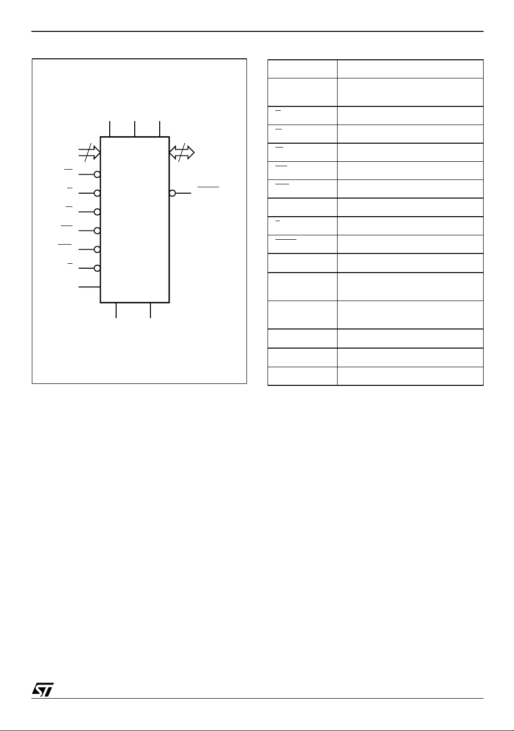
Figure 2. Logic Diagram Table 1. Signal Names
A0-A21 Address Inputs
A0-A21
W
RP
WP
DQ0-DQ15
V
V
DDQVPP
DD
22
16
DQ0-DQ15
E
WAIT
M58CR064C
G
M58CR064D
M58CR064P
E
G
W
RP
WP
KClock
L
Data Input/Outputs, Command
Inputs
Chip Enable
Output Enable
Write Enable
Reset/Power-Down
Write Protect
Latch Enable
M58CR064Q
WAIT
V
V
V
V
V
DD
DDQ
PP
SS
SSQ
L
K
V
SS
V
SSQ
AI90000
Wait
Supply Voltage
Supply Voltage for Input/Output
Buffers
Optional Supply Voltage for
Fast Program & Erase
Ground
Ground Input/Output Supply
NC Not Connected Internally
7/70
Page 8
M58CR064C, M58CR064D, M58CR064P, M58CR064Q
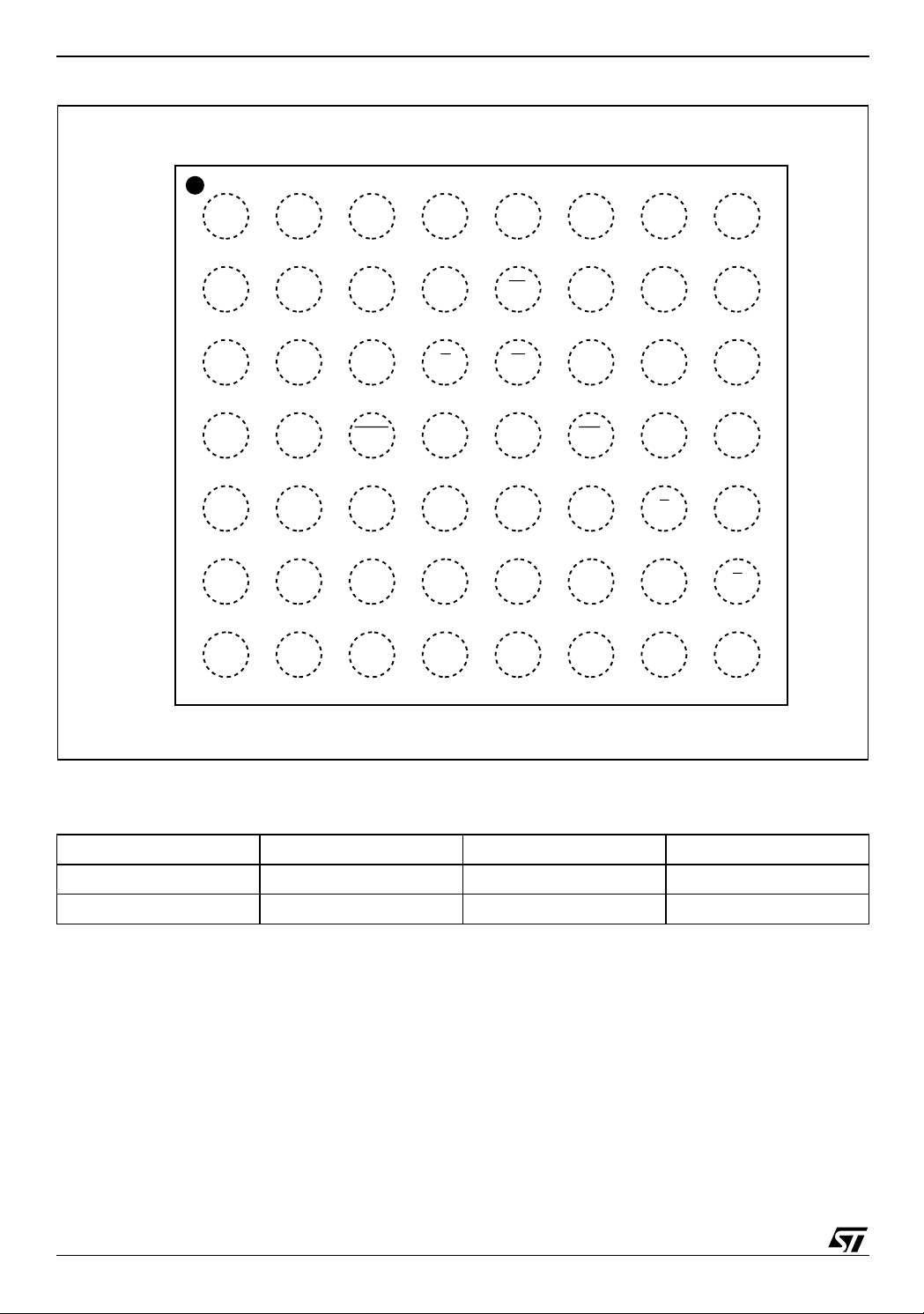
Figure 3. TFBGA Connections (Top view through package)
87654321
A
B
C A2
D A1
E
F
G
A13
A15
V
DDQ
V
SS
DQ7 V
A8A11
A9A12
A10
A14 WAIT A16 WP
DQ15
DQ14 DQ11 DQ10 DQ9 DQ0 G
SSQ
V
SS
A20
A21
DQ6
DQ13
DQ5 V
V
DD
K RP
L W
DQ4 DQ2 E A0
DD
V
PP
DQ12
DQ3
A18
DQ1
V
DDQ
A6
A5A17
A7A19
NC
DQ8
V
A4
A3
SSQ
Table 2. Bank Architecture
Bank A 16 Mbit 8 blocks of 4 KWord 31 blocks of 32 KWord
Bank B 48 Mbit - 96 blocks of 32 KWord
8/70
AI90001
Bank Size Parameter Blocks Main Blocks
Page 9
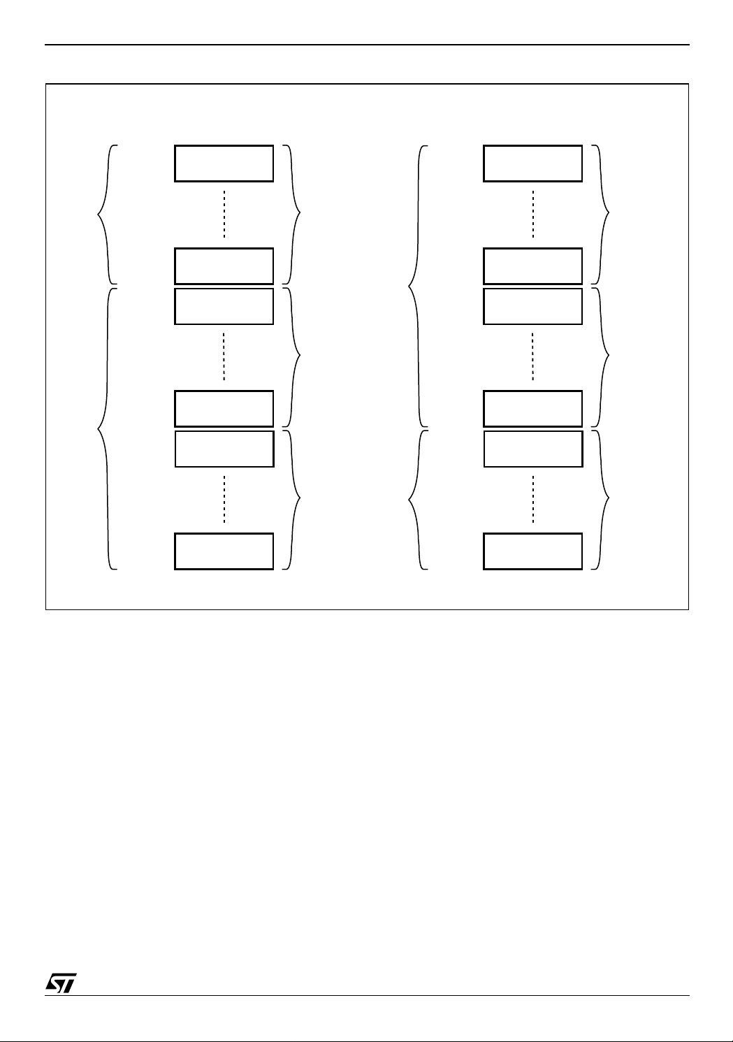
Figure 4. Me m ory Map
M58CR064C, M58CR064D, M58CR064P, M58CR064Q
Bank B
Bank A
000000h
007FFFh
2F8000h
2FFFFFh
300000h
307FFFh
3F0000h
3F7FFFh
3F8000h
3F8FFFh
3FF000h
3FFFFFh
Top Boot Block
Address lines A21-A0
512 Kbit or
32 KWord
512 Kbit or
32 KWord
512 Kbit or
32 KWord
512 Kbit or
32 KWord
64 Kbit or
4 KWord
64 Kbit or
4 KWord
Total of 96
Main Blocks
(bottom bank)
Total of 31
Main Blocks
(top bank)
Total of 8
Parameter
Blocks
(top bank)
Bank A
Bank B
000000h
000FFFh
007000h
007FFFh
008000h
00FFFFh
0F8000h
0FFFFFh
100000h
107FFFh
3F8000h
3FFFFFh
Bottom Boot Block
Address lines A21-A0
64 Kbit or
4 KWord
Total of 8
Parameter
Blocks
(bottom bank)
64 Kbit or
4 KWord
512 Kbit or
32 KWord
Total of 31
Main Blocks
(bottom bank)
512 Kbit or
32 KWord
512 Kbit or
32 KWord
Total of 96
Main Blocks
(top bank)
512 Kbit or
32 KWord
AI90002
9/70
Page 10

M58CR064C, M58CR064D, M58CR064P, M58CR064Q
SIGNAL DESCRIPTIONS
See Figure 2 Logic Diagram and Table 1,Signal
Names, for a brief overview of the signals connected to this device.
Address Inputs (A0-A21). The Address Inputs select the cells i n the memory array to a ccess during Bus Read operations. During Bus Write operations they control the commands sent to the Command Interface of the internal state machine.
Data Input/Output (DQ0-DQ15). The Data I/O outputs the data stored at the selected address during a Bus Read operation or inputs a command or the data to be programmed during a Bus Write operation.
Chip Enable (E
). The Chip Enable input acti-
vates the memory control logic, input buffers, decoders and sense amplifiers. When Chip Enable is
and Reset/Power-Down is at VIH the device
at V
IL
is in active mode. When Chip Enable is at V
IH
the
memory is deselected, the outputs are high impedance and the power consumption is reduced to the
stand-b y l e vel .
Output Enable (G
). The Output Enable controls
the outputs during the Bus Read operation of the
memory .
Write Enable (W
). The Write Enable controls the
Bus Write operation of the memory’s Command
Interface. The data and address inputs are latched
on the rising edge of Chip Enable or Write Enable
whichever occurs first.
Write Protect (WP
). Write Protect is an input
that gives an additional hardware protection for
each block. When Write Protect is at V
, the Loc k-
IL
Down is enabled and the prote ction status of t he
Locked-Down blocks cannot be changed. When
Write Protect is at V
, the Lock-Down is disabled
IH
and the Locked-Down blocks can be locked or unlocked. (refer to Table 13, Lock Status).
Reset/Power-Down (RP
). The Reset/Power-
Down input provides a hardware reset of the memory, and/or Power-Down functions, depending on
the Configuration Register status. When Reset/
Power-Down is at V
, the memory is in reset
IL
mode: the outputs are hi gh impedance an d if the
Power-Down function is enabled t he current consumption is reduced to the Reset Supply Current
I
. Refer to Table 18, DC Characte ristics - Cur-
DD2
rents for the value of I
After Reset all blocks
DD2.
are in the Locked state and the Configuration Register is reset. When Reset/Power-Down is at V
IH
the device is in normal operation. Exiting reset
mode the device enters asynchronous read mode,
but a negative transition of Chip Enable or Latch
Enable is required to ensure valid data outputs.
The Reset/Power-Down pin can be interfaced with
3V logic without any additional circuitry. It can be
tied to V
tics).
Latch Enable (L
dress bits on its rising edge. The a ddress latch is
transparent when Latch Enable is at V
hibited when Latch Enable is at V
can be kept Low (also at board level) when the
Latch Enable function is not required or supported.
Clo c k (K). The clock input synchronizes the memory to the microcontroller during synchronous read operations; the address is latched on a Clock edge (rising or falling, according to the configuration settings) when Latch Enable is at V don't care during asynchronous read and in write operations.
Wait (WAIT
synchronous read to indicate whether the dat a on
the output bus are valid. This output is high impedance when Chip Enable or Output Enable are at
V
or Reset/Power-Down is at VIL. It can be con-
IH
figured to be active during the wait cycle or one
clock cycle in advance.
Supply Voltage. VDD provides the power
V
DD
supply to the internal core of the memory device.
It is the main power supply for all operations
(Read, Program and Erase).
Supply Voltage. V
V
DDQ
supply to the I/O pins and enables all Outputs to
be powered independently from V
tied to V
Program Supply Vol t age . VPP is both a
V
PP
control input and a power supply pin. In
M58CR064C/D the two functions are s elected by
the voltage range applied to the pin. In the
M58CR064P/Q the control feature is disabled.
In M58CR064C/D if V
range (0V to V
In this case a voltage lower than V
absolute protection against program or erase,
while V
bles 18 and 19, DC Characteristics for the relevant
values). V
program or erase; a change in its value after the
operation has started does not have any effect and
program or erase operations continue.
If V
is in the rang e of V
PP
supply pin. In this condition V
til the Program/Erase algorithm is completed.
,
V
Ground. VSS ground is the reference for t he
SS
core supply. It must be connected to the system
ground.
Ground. V
V
SSQ
the input/output circuitry driven by V
must be connected to V
(refer to Table 19, DC Characteris-
RPH
). Latch Enable latches the ad-
IL
. Latch Enable
IH
). Wait is an output signal used during
provides the power
DDQ
. V
DD
or can use a separate supply.
DD
is kept in a low voltage
PP
) VPP is seen as a control input.
DDQ
PP
> V
enables these functions (see Ta-
PP1
is only sampled at the beginning of a
PP
it acts as a power
PPH
must be stable un-
PP
ground is the reference for
SSQ
SS
DDQ
PPLK
DDQ
and it is in-
. Clock is
IL
can be
gives an
. V
SSQ
10/70
Page 11
M58CR064C, M58CR064D, M58CR064P, M58CR064Q
Note: Each device in a system should have
V
DD, VDDQ
and VPP decoupled wi th a 0.1 µF ce-
ramic capacitor close to the pin (high frequency, inherently low inductance capacitors
should be as close as possible to the pack-
BUS OPERATIONS
There are six standard bus operations that control
the device. These are Bus Read , Bus Write, Address Latch, Output Disable, Standby and Reset.
See Table 3, Bus Operations, for a summary.
Typically glitches of less than 5ns on Chip Enable
or Write Enable are ignored by the memory and do
not affect Bus Write operations.
Bus Read. Bus Read operations are used to output the contents of the Memory Array, the Electronic Signature, the Status Register and the Common Flash Interface. Both Chip Enable and Output Enable must be at V
in order to perform a
IL
read operation. The Chip Enable input s hould be
used to enable the device. Out put Enable should
be used to gate data onto the output. The data
read depends on the previous command written to
the memory (see Command Interface section).
Refer to the Read AC Waveform figures and Characteristics tables in the DC and AC Parameters
section for details of when the output becomes valid.
Bus Write. Bus Write operations write Commands to the memory or latch Input Data to be programmed. A bus write operation is initiated when Chip Enable and Write Enable are at V Output Enable at V
. Commands, Input Data and
IH
IL
with
Addresses are latched on the rising edge of Write
Enable or Chip Enable, whichever occurs first. The
addresses can also be latched prior to the write
operation by toggling Latc h Enable. In this case
age). See Figure 9, AC Measurement Load Circuit. The PCB track widths should be sufficient
to carry the re quired V
program and erase
PP
currents.
the Latch Enable shoul d be t ied to V
during the
IH
bus write operation.
See Figures 14 and 15, Write AC Waveforms, and
Tables 22 and 23, Write AC Characteristics, for
details of the timing requirements.
Address Latch. Address latch operations input valid addresses. Both Chip enable and Latch Enable must be at V
during address latch opera-
IL
tions. The addresses are latched on the rising
edge of Latch Enable.
Output Disa bl e . The outputs are high impedance when the Output Enable is at V
.
IH
Standby. Standby di sables most of the internal circuitry allowing a substantial reduction of the current consumption. The memory is in stand-by when Chip Enable and Reset/Power-Down a re at
. The power consumption is reduced to the
V
IH
stand-by level and the ou tputs are se t to high impedance, independently from the Output Enable
or Write Enable inputs. If Chip Enable switches to
V
during a program or erase operation, t he de-
IH
vice enters Standby mode when finished. Reset. During Reset mode the memory is dese-
lected and the outputs are high impedance. The
memory is in Reset mode when Reset/PowerDown is at V
. The power consumption is reduced
IL
to the Standby leve l, inde pendent ly from t he Chip
Enable, Output Enable or Write Enable inputs. If
Reset is pulled to V
during a Program or Erase,
SS
this operation is aborted and the mem ory content
is no longer valid.
Table 3. Bus Operations
Operation E G W L RP WAIT DQ15-DQ0
Bus Read
Bus Write
Address Latch
Output Disable
Standby
Reset X X X X
Note: 1. X = Don’t care.
2. L
can be tied to VIH if the valid address has been previo usly latched.
3. Depends on G
V
IL
V
IL
V
IL
V
IL
V
IH
.
V
IL
V
IH
X
V
IH
XXX
V
IH
V
IL V
V
IH
V
IH
(2)
V
IL
(2)
IL
V
IL
X
V
IH
V
IH
V
IH
V
IH
V
IH
V
IL
Hi-Z Data Input
Data Output or Hi-Z
Hi-Z Hi-Z
Hi-Z Hi-Z
Hi-Z Hi-Z
Data Output
(3)
11/70
Page 12
M58CR064C, M58CR064D, M58CR064P, M58CR064Q
COMMAND INTERFACE
All Bus Write operations t o the me mory are in terpreted by the Command Interface. Commands
consist of one or more sequential Bus Write operations. An internal Program/Erase Controller handles all timings and verifies the correct execution
of the Program and Erase commands. The Program/Erase Controller provides a S tatus Register
whose output may be read at any ti me to monitor
the progress or the result of the operation.
The Command Interface is reset to read mode
when power is first applied, when exiting from Reset or whenever V
is lower than V
DD
LKO
. Command sequences must be followed exactly. Any
invalid combination of commands will reset the device to read mode.
Refer to Table 4, Command Codes and Appendix
D, Tables 36 and 37, Command Interface States Modify and Lock Tables, for a summary of the
Command Interface.
The Command Interface is split into two type s of
commands: Standard commands and Factory
Program commands. The following sections explain in detail how to perform each command.
Table 4. Command C odes
Hex Code Command
01h Block Lock Confirm
03h Set Configuration Register Confirm
10h Alternative Program Setup
20h Block Erase Setup
2Fh Block Lock-Down Confirm
30h Double Word Program Setup
40h Program Setup
50h Clear Status Register
55h Quadruple Word Program Setup
60h
70h Read Status Register
80h Bank Erase Setup
90h Read Electronic Signature
Block Lock Setup, Block Unlock Setup,
Block Lock Down Setup and Set
Configuration Register Setup
98h Read CFI Query
B0h Program/Erase Suspend
C0h Protection Register Program
D0h
FFh Read Array
Program/Erase Resume, Block Erase
Confirm, Bank Erase Confirm, Block
Unlock Confirm
12/70
Page 13

M58CR064C, M58CR064D, M58CR064P, M58CR064Q
COMMAND INTERFACE - STANDARD COMMANDS
The following commands are the basic commands
used to read, write to and configure the device.
Refer to Table 5, Standard Commands, in conjunction with the following text descriptions.
Read Array Command
The Read Array comm and returns the addressed
bank to Read Array mode. One Bus Write cycle is
required to issue the Read Array command and return the addressed bank to Read Array mode.
Subsequent read operations will read the addressed location and output t he data. A Read Array command can be issued in one bank while
programming or erasing in the other bank. However if a Read Array co mmand is issued to a bank
currently executing a Program or Erase operation
the command will be ignore d.
Read Status Register Command
A Bank’s Status Register indicates when a Program or Erase operation is complete and t he suc cess or failure of operation itself. Issue a Read
Status Register command to read the Status Register content of the addressed Bank. The Read
Status Register comma nd can be issued at any
time, even during Program or Erase operations.
The following Bus Read operations output the content of the Status Register of the addressed bank.
The Status Register is latched on the falling edge
or G signals, and can be read until E or G re-
of E
turns to V
date the latched data. See Table 8 for the
description of the Status Register Bit s. This m ode
supports asynchronous or single synchronous
reads only.
Read Electronic Signature Command
The Read Electronic Signature command reads
the Manufacturer and Device Codes, the Block
Locking Status, the Protection Register, and the
Configuration Register.
The Read Electronic Signature command consists
of one write cycle to an address within the bot tom
bank. A subsequent read operation in the address
of the bottom bank will output the Manufacturer
Code, the Device Code, the protection Status of
Blocks of the bottom bank, the Die Revision Code,
the Protection Register, or the Read Configuration
Register (see Table 6).
If the first write cycle of Read Electronic Signature
command is issued t o an address within the top
bank, a subsequent read operat ion in an address
of the top bank will output the protection Statu s of
blocks of the top bank. The status of the other
bank is not affected by the command (see Tab le
11). This mode supports asynchronous or sing le
synchronous reads only, it do es not support page
mode or synchronous burst reads.
. Either E or G must be toggled to up-
IH
Read CFI Query Command
The Read CFI Query command is used to read
data from the Common Flash Interface (CFI)
memory area located in the bottom bank. The
Read CFI Query Command consists of one Bus
Write cycle, to an address within the bottom bank.
Once the command is issued subsequent Bus
Read operations in the s ame bank read from the
Common Flash Interface.
If a Read CFI Query command is issued in a bank
that is executing a Program or Erase operation the
bank will go into Read Status Register mode, subsequent Bus Read cycles will output the Status
Register and the Program/Erase controller will
continue to Program or Erase in t he background.
When the Program or Erase operation has finished the device will enter Read CFI Query mode.
This mode supports asynchronous or single synchronous reads only, it does not support page
mode or synchronous burst reads.
The status of the other banks is not affected by the
command (see Table 11). After issuing a Read
CFI Query command, a Read Array command
should be issued to t he address ed bank to return
the bank to read mode.
See Appendix B, Common Flash Interface, Tables
30, 31, 32, 33, 34 and 35 for details on the in formation contained in the Co mmon Flash Interface
memory area.
Clear Status Register Command
The Clear Status Register comm and c an b e us ed
to reset (set to ‘0’) error bits SR1, SR3, SR4 and
SR5 in the Status Register of the addressed bank.
One bus write cycle is required to issue the Clear
Status Register command. After the Clear S tatus
Register command the bank returns to Read Array
mode.
The error bits in the Status Regi ster do not automatically return to ‘0’ when a new command is issued. The error bits i n the Stat us Register should
be cleared before attempting a new Program or
Erase command.
Block Erase Command
The Block Erase com mand can be used to erase
a block. It sets all the bits within the selected block
to ’1’. All previous d ata in th e block is lost. If th e
block is protected then the Erase operation will
abort, the data in the block will not be changed and
the Status Register will output the error. The Block
Erase command can be issued at any moment, regardless of whether the block has been programmed or not.
Two Bus Write cycles are required to issue the
command.
■ The first bus cycle sets up the Erase command.
13/70
Page 14

M58CR064C, M58CR064D, M58CR064P, M58CR064Q
■ The second latches the block address in the
internal state machine and starts the Program/
Erase Controller.
If the second bus cycle is not Write Erase Confirm
(D0h), Status Register bits SR 4 and SR5 are set
and the command aborts. Erase aborts if Reset
turns to V
. As data integrity cannot be guaran-
IL
teed when the Erase operation is aborted, the
block must be erased again.
Once the command is issued the device outputs
the Status Register data when any address within
the bank is read. At the end o f the operation the
bank will remain in Read Status Register mode until a Read A rray, Read CFI Query o r Read Electronic Signature command is issued.
During Erase operations the bank containing the
block being erased will onl y ac cept the Read Status Register and the Program/Erase Suspend
command, all other commands will be ignored.
Refer to Dual Operations section for detailed information about simultaneous operations allowed in
banks not being erased. Typical Erase times are
given in Table 14, Program, Erase Times and Program/Erase Endurance Cycles.
See Appendix C, Figure 24, Block Erase Flowchart and Pseudo Code, for a suggested flowchart
for using the Block Erase command.
Program Command
The memory array can be programmed word-byword. Only one Word in one bank can be programmed at any one time. Two bus write cycles
are required to issue the Program Command.
■ The first bus cycle sets up the Program
command.
■ The second latches the Address and the Data to
be written and starts the Program/Erase
Controller.
After programming has started, read operations in
the bank being programmed output the Status
Register content.
During Program operations the bank being programmed will only accept the Read Statu s Register and the Program/Erase Suspend command.
Refer to Dual Operations section for detailed information about simultaneous operations allowed in
banks not being programmed. Typical Program
times are given in Table 14, Program, Erase
Times and Program/Erase Endurance Cycles.
Programming aborts if Reset goe s to V
. As data
IL
integrity cannot be guaranteed when the program
operation is aborted, the memory location must be
reprogrammed.
See Appendix C, Figure 20, Program Flowchart
and Pseudo Code, for the f lowchart for using the
Program command.
Program/Erase Suspend Command
The Program/Erase Suspend command is used to
pause a Program or Block Erase operation. A
Bank Erase operation cannot be suspended.
One bus write cycle is required to issue t he Program/Erase Suspend command. Once the Program/Erase Controller has paused bits SR7 , SR6
and/ or SR2 of the Status Register will be set to ‘1’.
The command must be addressed to the bank
containing the Program or Erase operation.
During Program/Erase Suspend the Command Interface will accept the Program/Erase Resume,
Read Array (cannot read the suspended block),
Read Status Register, Read Electronic S ignature
and Read CFI Q uery commands. Additionally, if
the suspend operation was Erase then the Clear
status Register, Program, Block Lock, Block LockDown or Protection Program commands wi ll also
be accepted. The block being erased may be protected by issuing the Block Lock, Block LockDown or Protection Register Program commands.
Only the blocks not being e rased m ay be read or
programmed correctly. When the Program /Erase
Resume command is issued the operation will
complete. Refer to the Dual Operations section for
detailed information about simultaneous operations allowed during Program/Erase Suspend.
During a Program/Erase Suspend, the device can
be placed in standby mode by taking Chip Enable
. Program/Erase is aborted if Reset turns to
to V
IH
V
.
IL
See Appendix C, Figure 23 , Program Suspend &
Resume Flowchart and Pseudo Code, and Figure
25, Erase Suspend & Resume Flowchart and
Pseudo Code for flowcharts for using the Program/
Erase Suspend command.
Program/Erase Resu me Command
The Program/Erase Resume command can be
used to restart the Program/Erase Controller after
a Program/Erase Suspen d command has paused
it. One Bus Write cycle is required to issue the
command. The comm and must be written to the
bank containing the Program or Erase Suspend.
The Program/Erase Resume command changes
the read mode of th e target bank to Read S tatus
Register mode.
If a Program command is iss ued during a Block
Erase Suspend, then the erase cannot be resumed until the programming operation has completed. It is possible to accumulate suspend
operations. For example: su spend an erase operation, start a programming operation, suspend the
programming operation then read the array. See
Appendix C, Figure 23, Program Su spend & Resume Flowchart and Pseudo Code, and Figure 25,
Erase Suspend & Resume Flowchart and Pseudo
14/70
Page 15

M58CR064C, M58CR064D, M58CR064P, M58CR064Q
Code for flowcharts for using the Program/Erase
Resume command.
Protection Regi ster Pr ogram Com m and
The Protection Register Program command is
used to Program the 128 bit user O ne-Time-Programmable (OTP) segment of the Protection Register. The segment is programmed 16 bits at a
time. When shipped all bits in the segment are set
to ‘1’. The user can only program the bits to ‘0’.
Two write cycles are required to issue the Protec-
tion Register Program command.
■ The first bus cycle sets up the Protection
Register Program command.
■ The second latches the Address and the Data to
be written to the Protection Register and starts
the Program/Erase Controller.
Read operations output the Status Register content after the programming has started.
The segment can be protected by programming bit
1 of the Protection Lock Register. Bit 1 of the Protection Lock Register also protects bit 2 of the Protection Lock Register. Programming bit 2 of the
Protection Lock Register will result in a permanent
protection of Parameter Block #0 (see Figure 5,
Security Block and Protection Register Memory
Map). Attempting to program a previously protected Protection Register will result in a Status Register error. The protection of the Protection
Register and/or the Security Block is not reversible.
The Protection Register Program cannot be suspended. See Appendix C, Figure 27, Protection
Register Program Flowchart and Pseudo Code,
for a flowchart for using the Protection Register
Program command.
Set Conf ig uration Regi s te r C om m and.
The Set Configuration Register command is used
to write a new value to the Configuration Control
Register which defines the burst length, type, X latency, Synchronous/Asynchronous Read mode
and the valid Clock edge configuration.
Two Bus Writ e cycles a re required to i ssue the Set
Configuration Register command.
■ The first cycle writes the setup command and
the address corresponding to the Configuration
Register content.
■ The second cycle writes the Configuration
Register data and the confirm command.
Once the comman d is issued the memory ret urns
to Read mode.
The value for the Configuration Register is always
presented on A0-A15. CR0 is on A0, CR1 on A1,
etc.; the other address bits are ignored.
Block Lock Command
The Block Lock command is used to lock a block
and prevent Program or Erase operations from
changing the data in it. All blocks are locked at
power-up or reset.
Two Bus Write cycles are required to issue the
Block Lock command.
■ The first bus cycle sets up the Block Lock
command.
■ The second Bus Write cycle latc hes the block
address.
The lock status can be monitored for each block
using the Read Electronic Signature command.
Table. 13 shows the Lock Status after issuing a
Block Lock command.
The Block Lock bits are vo latile, once set they remain set until a hardware reset or power-down/
power-up. They are cleared by a Block Unlock
command. Refer to the section, Block Locking, for
a detailed explanation. See Appendix C, Figure
26, Locking Operations Flowchart and Pseudo
Code, for a flowchart for using the Lock command.
Block Unlock Command
The Block Unlock command is used to unlock a
block, allowing the block to be programmed or
erased. Two Bus Write cycles are requ ired to issue the Block Unlock command.
■ The first bus cycle sets up the Block Unlock
command.
■ The second Bus Write cycle latc hes the block
address.
The lock status can be monitored for each block
using the Read Electronic Signature command.
Table 13 shows the protection status after issuing
a Block Unlock command. Refer to the section,
Block Locking, for a detailed expla nation and A ppendix C, Figure 26, Locking Operations Flowchart and Pseudo Code, f or a flowchart for using
the Unlock command.
Block Lock-Down Command
A locked or unlocked block can be locked-down by
issuing the Block Lock-Down command. A lockeddown block cannot be programm ed or erased, or
have its protection status changed when WP
low, V
. When WP is high, V
IL
the Lock-Down
IH,
is
function is disabled and the locked blocks can be
individually unlocked by the Block Unlock command.
Two Bus Write cycles are required to issue the
Block Lock-Down command.
■ The first bus cycle sets up the Block Lock
command.
■ The second Bus Write cycle latc hes the block
address.
15/70
Page 16
M58CR064C, M58CR064D, M58CR064P, M58CR064Q
The lock status can be monitored for each block
using the Read Electronic Signature command.
Locked-Down blocks revert to the locked (and not
locked-down) state when the device is reset on
power-down. Table. 13 shows the Lo ck Statu s af-
ter issuing a Block Lock-Down command. Refer to
the section, Block Locking, for a detailed explanation and Appendix C, Fi gure 26, Locking Operations Flowchart and Pseudo Code, for a flowchart
for using the Lock-Down command.
Table 5. Standard Commands
Bus Operations
Commands
Cycles
Read Array 1+ Write BKA FFh
Read Status Regist er 1+ Write BKA 70h Read
Read Electronic Signature 1+ Write
Read CFI Query 1+ Write BBKA 98h Read
Clear Status Register 1 Write BKA 50h
Block Erase 2 Write B KA 20h Write BA D0h
Program 2 Write BKA 40h or 10h Write WA PD
Program/E rase Su s pen d 1 Wr i te BKA B0h
Program/Erase Resume 1 Write BKA D0h
Protection Register Program 2 Write PRA C0h Write
Set Configuration Register 2 Write CRD 60h Write
Block Lock 2 Write BKA 60h Write
Block Unlock 2 Write BKA 60h Write
Block Lock-Down 2 Write BKA 60h Write
Note: 1. X = Don’t Care, WA=Word Address in targeted bank, RD=Read Data, SRD=Status Register Data, ESD=Electronic Signature Data,
QD=Query Data, BA=Block Address, BKA= Bank Address, BBKA= Bottom Bank Address, PD=Program Data, PRA=Protection
Register Address, PRD=Protection Register Data, CRD=Configuration Register Data.
2. Must be same bank as in the first cycle. The signature address es are listed i n T able 6.
3. When addre ss ed to a block i n th e T op Bank, re ads Block Prot ection data only.
Op. Add Data Op. Add Data
1st Cycle 2nd Cycle
BBKA or
(3)
BKA
Read
90h Read
WA RD
(2)
BKA
BBKA or
(2,3)
BKA
(2)
BBKA
PRA PRD
CRD
BA 01h
BA D0h
BA
SRD
ESD
QD
03h
2Fh
(3)
16/70
Page 17
M58CR064C, M58CR064D, M58CR064P, M58CR064Q
Table 6. Electronic Signature Codes
Code Address (h) Data (h)
Manufacturer Code Bottom Bank Address + 00 0020
Top (M58CR064C)
88CA
Bottom (M58CR064D) 88CB
Device Code
Bottom Bank Address + 01
Top (M58CR064P) 8801
Bottom (M58CR064Q) 8802
Lock
0001
Unlocked 0000
Block Protection
Block Address + 02
Locked and Locked-Down 0003
Unlocked and Locked-Down 0002
Reserved Bottom Bank Address + 03 Reserved
Configuration Register Bottom Bank Address + 05 CR
ST Factory Default
xx06
Security Block Permanently Locked xx02
Protection Register Lock
OTP Area Permanently Locked xx04
Security Block and OTP Area Permanently
Locked
Bottom Bank Address + 80
Bottom Bank Address + 81
Bottom Bank Address + 84
xx00
Unique Device
Number
Protection Register
Bottom Bank Address + 85
Bottom Bank Address + 8C
Note: CR=Conf ig uration Regi ster.
OTP Area
Figure 5. Security Block and Protection Register Memory Map
PROTECTION REGISTER
8Ch
SECURITY BLOCK
85h
84h
Parameter Block # 0
81h
80h
User Programmable OTP
Unique device number
Protection Register Lock 2 1 0
AI06181
17/70
Page 18

M58CR064C, M58CR064D, M58CR064P, M58CR064Q
COMMAND INTERFACE - FACTORY PROGRAM COMMANDS
The Factory Program commands are used to
speed up programming. They require V
V
except for the Bank Eras e command which
PPH
also operates at V
= VDD. Refer to Table 7, Fac-
PP
to be at
PP
tory Program Commands, in conjunction with the
following text descriptions.
Bank Erase Command
The Bank Erase command can be used to erase a
bank. It sets all the bits within the selected bank to
’1’. All previous data in th e ban k is lo st. Th e B ank
Erase command will igno re any protected blocks
within the bank. If all blocks in the ba nk are protected then the Bank Erase operation will abort
and the data in the bank wi ll not b e changed. The
Status Register will not output any error.
Bank Erase operations can be p erformed at both
= V
V
PP
and VPP = VDD.
PPH
Two Bus Write cycles are required to issue the
command.
■ The first bus cycle sets up the Bank Erase
command.
■ The second latches the bank address in the
internal state machine and starts the Program/
Erase Controller.
If the second bus cycle is not Write Bank Erase
Confirm (D0h), Status Register bits SR4 and S R5
are set and the command aborts. Erase aborts if
Reset turns to V
. As data integrity cannot be
IL
guaranteed when the Erase operation is aborted,
the bank must be erased again.
Once the command is issued the device outputs
the Status Register data when any address within
the bank is read. At the end o f the operation the
bank will remain in Read Status Register mode until a Read Array, Read CFI Query or Read Electronic Signature command is issued.
During Bank Erase operations the bank being
erased will only accept the Read Status Regi ster
command, all other commands w ill be ignored . A
Bank Erase operation cannot be suspended.
For optimum performance, Bank Erase commands should be limited to a maximum of 100 Program/Erase cycles per Block. After 100 Program/
Erase cycles the internal algorithm will still operate
properly but some degradation in performance
may occur.
Dual operations are not supported during Bank
Erase operations and the command cannot be
suspended.
Typical Erase times are given in Table 14, Program, Erase Times and Program/Erase Endurance Cycles.
Double Word Program Command
The Double Word Program command improves
the programming throughput by writing a page of
two adjacent words in parallel. The two words
must differ only for the address A0.
Programming should not be attempted when V
is not at V
V
is below V
PP
Three bus write cycles are necessary to issue the
Double Word Program command.
■ The first bus cycle sets up the Double Word
Program Command.
■ The second bus cycle latches the Address and
the Data of the first word to be written.
■ The third bus cycle latches the Address and the
Data of the second word to be written and starts
the Program/Erase Controller.
Read operations in the bank bei ng programmed
output the Status Register content after the programming has started.
During Double Word Program operations the bank
being programmed will only a ccept the Read Status Register command, all other commands will be
ignored. Dual operations are not supported during
Double Word Program operations. It is not recommended to suspend the Double Word Program
command. Typical Program times are given in Table 14, Program, Erase Times and Program/Erase
Endurance Cycles.
Programming aborts if Reset goe s to V
integrity cannot be guaranteed when the program
operation is aborted, the memory locations m ust
be reprogrammed.
See Appendix C, Figure 21, Double Word Program Flowchart and Pseudo Code, for the flowchart for using the Double Word Program
command.
Quadruple Word Program Command
The Quadruple Word Program command improves the programming throughput by writing a
page of four adjacent words in parallel. The four
words must differ only for the addresses A0 and
A1.
Programming should not be attempted when V
is not at V
is below V
V
PP
Five bus write cycles are necessary to issue the
Quadruple Word Program command.
■ The first bus cycle sets up the Double Word
Program Command.
■ The second bus cycle latches the Address and
the Data of the first word to be written.
. The command can be executed if
PPH
PPH
but the result is not guaranteed.
PPH
IL
. The command can be executed if
but the result is not guaranteed.
PPH
PP
. As data
PP
18/70
Page 19
M58CR064C, M58CR064D, M58CR064P, M58CR064Q
■ The third bus cycle latches the Address and the
Data of the second word to be written.
■ The fourth bus cycle latches the Address and
the Data of the third word to be written.
■ The fifth bus cycl e latches the Addr es s and the
Data of the fourth word to be written and starts
the Program/Erase Controller.
Read operations to the bank being programmed
output the Status Register content after the programming has started.
Programming aborts if Reset goe s to V
. As data
IL
integrity cannot be guaranteed when the program
operation is aborted, the memory locations mu st
be reprogrammed.
During Quadruple Word Program operations the
bank being programmed will only accept the Read
Status Register command, all other commands
will be igno re d.
Dual operations are not supported during Quadruple Word Program operations. It is not recommended to suspend the Quadruple Word Program
command. Typical Program times are given in Table 14, Program, Erase Times and Program/Erase
Endurance Cycles.
See Appendix C, Figure 22, Quadruple Word Program Flowchart and Pseudo Code, for the flowchart for using the Quadruple Word Program
command.
Table 7. Factory Program Commands
Bus Write Operations
Command Phase
Cycles
Bank Eras e 2 BKA 80h BKA D0h
(2)
Double Wor d Program
Quadruple Word
Program
Note: 1. WA=Word A dd ress in t arget ed bank, BKA= Bank A d dress, PD = P r ogram Data, WA1 is t h e S t a rt Addr e s s.
(3)
2. Word Addres ses 1 and 2 must be consecutive Addresses differing only for A0.
3. Word Addres ses 1,2,3 and 4 must be consecutive Addresses di ffering onl y for A0 and A1.
3 BKA 30h WA1 PD1 WA2 PD2
5 BKA 55h WA1 PD1 WA2 PD2 WA3 PD3 WA4 PD4
1st 2nd 3rd 4th 5th
Add Data Add Data Add Data Add Data Add Data
19/70
Page 20

M58CR064C, M58CR064D, M58CR064P, M58CR064Q
STATUS REGISTER
The M58CR064 has two Status Registers, one for
each bank. The Status Registers provide information on the current or previous Program or Erase
operations executed in each bank. Issue a Read
Status Register command to read the contents of
the Status Register, refer to Read Status Register
Command section for more details. To output the
contents, the Status Register is latched and updated on the falling edge of the Chip Enable or Output
Enable signals, and can be read until Chip Enable
or Ou tpu t Enable return s to V
. The Status Reg-
IH
ister can only be read using single asynchronous
or single synchronous reads. Bus Read operations from any address within the bank, always
read the Status Register during Program and
Erase operations.
The various bits convey information about the status and any errors of the operation. Bits SR7, SR6
and SR2 give information on the status of the bank
and are set and reset by the device. Bits SR5,
SR4, SR3 and SR1 give information on errors,
they are set by the device but must be reset by issuing a Clear Status Register command or a hard-
ware reset. If an error bit is set to ‘1’ the Status
Register should be reset before issuing another
command.
The bits in the Status Register are summarized in
Table 8, Status Register Bits. Refer to Table 8 in
conjunction with the following text descriptions.
Program/Erase Controller Status Bit (SR7). The
Program/Erase Controller Status bit indicates
whether the Program/Erase Controller is act ive or
inactive in the addressed bank. When the Program/Erase Controller Status bit is Low (set to ‘0’),
the Program/Erase Controller is active; when the
bit is High (set to ‘1’), the Prog ram/E rase Cont roller is inactive, and the device is ready to process a
new command.
The Program/Erase Controller Status is Low immediately after a Program/Erase Suspend command is issued until the Program/Erase Controller
pauses. After the Program/Erase Controller pauses the bit is High.
During Program, Erase, o perations the Program/
Erase Controller Status bit can be polled to find the
end of the operation. Other bits in the Status Register should not be tested until the Program/Erase
Controller completes the operation and the bit is
High.
After the Program/Erase Cont roller completes its
operation the Erase Status, Prog ram Status, V
PP
Status and Block Lock Status bits should be tested
for errors.
Erase Suspend Status Bit (SR6). The Erase
Suspend Status bit indicates that an Erase operation has been suspended or is going to be sus-
pended in the addressed block. When the Eras e
Suspend Status bit is High (set to ‘1’), a Program/
Erase Suspend command has been issued and
the memory is waiting for a Program/Erase Resume command.
The Erase Suspend Status should only be considered valid when the Program/Erase Controller Status bit is High (Program/Erase Controller inactive).
SR7 is set within 30µs of the Program/Erase Suspend command being issued therefore the memory may still complete the operation rather than
entering the Suspend mode.
When a Program/Erase Re sume command is issued the Erase Suspend Status bit returns Low.
Erase Status Bit (SR5). The Erase Status bit
can be used to identify if the memory has failed to
verify that the block or bank has erased correctly.
When the Erase Status b it is High (set to ‘1’), the
Program/Erase Controller has applied the maximum number of pulses to the block or bank and
still failed to verify that it has erased correctly. The
Erase Status bit should be read once the Program/
Erase Controller Status bit is High (Program/Erase
Controller inactive).
Once set High, the Erase Status bit can only be reset Low by a Clear Status Register command or a
hardware reset. If set High it should be reset before a new Program or Erase command is issued,
otherwise the new command will appear to fail.
Program Status Bit (SR4). The Program Status
bit is used to identify a Pr ogram failure. When the
Program Status bit is High (set to ‘1’), the Program/Erase Controller has applied the maximum
number of pulses to the byte and still failed to verify that it has programmed correctly. The Program
Status bit should be read once the Program/Erase
Controller Status bit is High (Program/Erase Controller inactive).
Once set High, the Program Status bit can only be
reset Low by a Clear Status Register command or
a hardware reset. If set High it should be reset before a new command is issued, otherwise the new
command will appear to fail.
Status Bit (SR3). The VPP Status bit can be
V
PP
used to identify an invalid v oltage on the V
during Program and Erase operations. The V
pin is only sampled at the beginning of a Program
or Erase operation. Indeterminate results can occur if V
When the V
age on the V
when the V
pin has a voltage that is below the VPP Lockout
Voltage, V
gram and Erase operations cannot be performed.
becomes invalid during an operation.
PP
Status bit is Low (set to ‘0’), the volt-
PP
pin was sampled at a valid voltage;
PP
Status bit is High (set to ‘1’), the V
PP
, the memory is protected and Pro-
PPLK
PP
pin
PP
PP
20/70
Page 21
M58CR064C, M58CR064D, M58CR064P, M58CR064Q
Once set High, the VPP Status bit can only be reset
Low by a Clear Status Register command or a
hardware reset. If set High it should be reset before a new Program or Erase command is issued,
otherwise the new command will appear to fail.
Program Suspend Status Bit (SR2). The Program Suspend Status bit indicates that a Program
operation has been suspended in the addressed
block. When the Program Suspend Status bit is
High (set to ‘1’), a Program/Erase Suspend command has been issued and the memory is waiting
for a Program/Erase Resume command. The Program Suspend Status should only be considered
valid when the Program/Erase Controller Status
bit is High (Program/Erase Controller inactive).
SR2 is set within 5µs of the Program/Erase Suspend command being issued therefore the memo-
When a Program/Erase Re sume command is issued the Program Suspend Status bit returns Low.
Block Protection Status Bit (SR1). The Block
Protection Status bit can be used to identify if a
Program or Block Erase operation has tried to
modify the contents of a locked block.
When the Block Protection Status bit is High (set
to ‘1’), a Program or Erase operation has been attempted on a locked block.
Once set High, the Block Protection Status bit can
only be reset Low by a Clear Status Register command or a hardware reset. If set High it should be
reset before a new command is issued, otherwise
the new command will appear to fail.
Reserved Bit (SR0). SR0 is reserved. Its value
must be masked.
ry may still complete the operation rather than
entering the Suspend mode.
Table 8. Status Register Bits
Bit Name Type Logic Level Definition
SR7 P/E.C. Status Status
SR6 Erase Suspend Status Status
SR5 Erase Status Error
’1’ Ready
’0’ Busy
’1’ Erase Suspended
’0’ Erase In progress or Completed
’1’ Erase Error
’0’ Erase Success
SR4 Program Status Error
Status
V
SR3
SR2 Program Suspend Status Status
SR1 Block Protection Status Error
SR0 Reserved
Note: Logic level ’1’ is High, ’0’ is Low.
PP
Error
’1’ Program Error
’0’ Program Success
V
’1’
’0’
’1’ Program Suspended
’0’ Program In Progress or Completed
’1’ Program/Erase on protected Block, Abort
’0’ No operation to protected blocks
Invalid, Abort
PP
OK
V
PP
21/70
Page 22

M58CR064C, M58CR064D, M58CR064P, M58CR064Q
CONFIGURATION REGISTER
The Configuration Register is used to configure
the type of bus access that the memory will perform. Refe r to Rea d Mo des secti on fo r d etai ls on
read operations.
The Configuration Register is set through the
Command Interface. After a Reset or Power-Up
the device is configured for asynchronous page
read (CR15 = 1). T he Configuration Register bits
are described in Table 9. They spe cify the selection of the burst length, burst type, burst X latency
and the Read operation. Refer to Figures 6 and 7
for examples of synchronous burst configurations.
Read Select Bit (CR15)
The Read Select bit, CR15, is used to switch between asynchronous an d sync hronous B us Read
operations. When the Read Se lect bit is set to ’1’,
read operations are asynchronous; when the
Read Select bit is set to ’0’, read o perations are
synchronous. Synchronous Burst Read is supported in both parameter and main blocks and can be
performed across banks.
On reset or power-up the Read Sel ect bit is set
to’1’ for asynchronous access.
X-Latency Bits (CR13-CR11)
The X-Latency bits are used during Synchronous
Read operations to set the number of clock cycles
between the address bei ng latched and the first
data becoming available. For correct operation the
X-Latency bits can only assume the values in Table 9, Configuration Register.
The correspondence be tween X-Latency settings
and the maximum sustainable freq uency must be
calculated taking into account some system parameters. Two conditions must be satisfied:
1. Depending on whether t
AVK_CPU
or t
DELAY
is
supplied either one of the following two
equations must be satisfied:
(n + 1) t
(n + 2) tK ≥ t
≥ t
ACC
ACC
- t
AVK_CPU
+ t
DELAY
K
+ t
+ t
QVK_CPU
QVK_CPU
2. and also
> t
t
K
KQV
+ t
QVK_CPU
where
n is the chosen X-Latency configuration code
is the clock period
t
K
t
AVK_CPU
is clock to address valid, L Low, or E
Low, whichever occurs last
t
is address valid, L Low, or E Low t o clock,
DELAY
whichever occurs last
t
QVK_CPU
is the data setup time required by the
system CPU,
is the clock to data valid time
t
KQV
is the random access time of the device.
t
ACC
Refer to Figure 6, X-Latency and Data Output
Configuration Example.
Power-Do wn Bit (CR10 )
The Power-Down bit is used to enable or di sable
the power-down function.
When the Power-Down bit is set to ‘0’ the powerdown function is disabled. If the Reset/PowerDown, RP
and the supply current, I
standby value, I
When the Power-Down bit is set to ‘1’ the powerdown function is enabled. If the Reset/PowerDown, RP
the power-down state and the supply current, I
is reduced to the power-down value, I
The recovery time after a Reset/Power-Down, RP
pulse is significantly longer when power-down is
enabled (see Table 24).
After a reset the Power-Down Bit is set to ‘0’.
Wait Co nf i gur a tio n B it (CR 8)
In burst mode the Wait bit controls the timing of the
Wait output pin, WAIT
Wait output pin is asserted during th e wait state.
When the Wait bi t is ’1’ (default) the W ait output
pin is asserted one clock cycle before the wait
state.
is asserted during a continuous burst and
WAIT
also during a 4 or 8 burst length if no-wrap configuration is selected. WAIT
asynchronous reads, single synchronous reads or
during latency in synchronous reads.
Burst Type Bit (CR7)
The Burst Type bit is used to configure the sequence of addres ses read as sequential or interleaved. When the Burst Type bit is ’0’ the memory
outputs from interleaved addresses; when the
Burst Type bit is ’1’ (default) the mem ory outputs
from sequential addresses. Se e Tables 10, Burst
Type Definition, for the sequence of addresses
output from a given starting address in each mode.
Valid Clock Edge Bit (CR6)
The Valid Clock Edge bit, CR6, is used to configure the active edge of the Clock, K, during Synchronous Burst Read operations. When the Valid
Clock Edge bit is ’0’ the falling edge of the Clock is
the active edge; when the Vali d Clock Edge bit is
’1’ the rising edge of the Clock is active.
Wrap Burst Bit (CR3)
The burst reads can be confined inside the 4 or 8
Word boundary (wrap) or o vercome t he b oundary
(no wrap). The Wrap Burst bit i s used t o sel ect between wrap and no wrap. When the Wrap Burst bit
is set to ‘0’ the burst read wraps; when it is set to
‘1’ the burst read does not wrap.
, pin goes Low, VIL, the device is reset
is reduced to the
DD,
DD3
.
, pin goes Low, VIL, the device goes into
DD,
.
DD2
. When the Wait bit is ’0’ the
is not asserted during
,
22/70
Page 23

M58CR064C, M58CR064D, M58CR064P, M58CR064Q
Burst length Bits (CR2-CR0)
The Burst Length bits set the n umb er of Words t o
be output during a Synchronous Burst Read operation as result of a single address latch cycle.
They can be set for 4 words, 8 words or continuous burst, where all the words are read sequentially.
In continuous burst mode the burs t sequ ence c an
cross bank boundaries.
In continuous burst mode or in 4, 8 words no-wrap,
depending on the starting add ress, the dev ice a s serts the WAIT
output to indicate that a delay is
necessary before the data is output.
Table 9. Configuration Register
Bit Description Value Description
CR15 Read Select
CR14 Reserved
CR13-CR11 X-Latency
0 Synch rono us Re ad
1 Asynchronous Read (Default at power-on)
010 2 clock latency
011 3 clock latency
100 4 clock latency
101 5 clock latency
111 Reserved
Other configurations reserved
If the starting address is aligned to a 4 word
boundary no wait states are needed and the WAIT
output is not asserted.
If the starting address is shifted by 1,2 or 3 positions from the four word boundary, WAIT
will be
asserted for 1, 2 or 3 clock cycles when the burst
sequence crosses the first 64 word b oundary, to
indicate that the device needs an internal delay to
read the successive words in the array. WAIT
will
be asserted only once during a continuous burst
access. See also Table 10, Burst Type Definition.
CR14, CR9, CR5 and CR4 are reserved for future
use.
CR10
CR9 Reserved
CR8 Wait Configuration
CR7 Burst Type
CR6 Valid Clock Edge
CR5-CR4 Reserved
CR3 Wrap Burst
CR2-CR0 Burst Length
Power-Down
0 Power-Down disabled
1 Power-Down enabled
0
1
0 Interleaved
1 Sequential (default)
0 Falling Clock edge
1 Rising Clock edge
0 Wrap
1 No W rap
001 4 words
010 8 words
111 Continuous (CR7 must be set to ‘1’)
WAIT is active during wait state
WAIT is active one data cycle before wait state (default)
23/70
Page 24

M58CR064C, M58CR064D, M58CR064P, M58CR064Q
Table 10. Burst Type Definition
Start
Address 4 Words 8 Words
Mode
Sequential Interleaved Sequential Interleaved
0 0-1-2-3 0-1-2-3 0-1-2-3-4-5-6-7 0-1-2-3-4-5-6-7 0-1-2-3-4-5-6...
1 1-2-3-0 1-0-3-2 1-2-3-4-5-6-7-0 1-0-3-2-5-4-7-6 1-2-3-4-5-6-7...
2 2-3-0-1 2-3-0-1 2-3-4-5-6-7-0-1 2-3-0-1-6-7-4-5 2-3-4-5-6-7-8...
3 3-0-1-2 3-2-1-0 3-4-5-6-7-0-1-2 3-2-1-0-7-6-5-4 3-4-5-6-7-8-9...
...
7 7-4-5-6 7-6-5-4 7-0-1-2-3-4-5-6 7-6-5-4-3-2-1-0 7-8-9-10-11-12-13...
Wrap
...
60 60-61-62-63-64-65-66...
61 61-62-63-WAIT-64-65-66...
62 62-63-WAIT-WAIT-64-65-66...
63
Sequential Interleaved Sequential Interleaved
0 0-1-2-3 0-1-2-3-4-5-6-7
Continuous Burst
63-WAIT-WAIT-WAIT-64-65-
66...
1 1-2-3-4 1-2-3-4-5-6-7-8
2 2-3-4-5 2-3-4-5-6-7-8-9...
3 3-4-5-6 3-4-5-6-7-8-9-10
...
7 7-8-9-10 7-8-9-10-11-12-13-14
...
No-wrap
60 60-61-62-63
61 61-62-63-WAIT-64
62-63-WAIT-WAIT-
62
63
63-WAIT-WAITWAIT-64-65-66
64-65
60-61-62-63-64-65-66-
61-62-63-WAIT-64-65-
66-67-68
62-63-WAIT-WAIT-64-
65-66-67-68-69
63-WAIT-WAIT-WAIT-
64-65-66-67-68-69-70
Same as for Wrap
(Wrap /No Wrap
has no effect on
Continuous Burst )
67
24/70
Page 25

M58CR064C, M58CR064D, M58CR064P, M58CR064Q
Figure 6. X-Latency a nd Da ta Ou t put C on f ig uration Exam pl e
X-latency
1st cycle 2nd cycle 3rd cycle 4th cycle
K
E
L
A21-A0 VALID ADDRESS
tDELAY
DQ15-DQ0
Note. Settings shown: X-latency = 4, Data Output held for one clock cycle
tAVK_CPU tKtQVK_CPU
tACC
Figure 7. Wai t Co nf i g ura tio n Exampl e
E
K
L
A21-A0
VALID ADDRESS
VALID DATA
tQVK_CPUtKQV
VALID DATA
AI90005
DQ15-DQ0
WAIT
CR8 = '0'
WAIT
CR8 = '1'
VALID DATA
VALID DATA NOT VALID VALID DATA
AI90006b
25/70
Page 26

M58CR064C, M58CR064D, M58CR064P, M58CR064Q
READ MODES
Read operations can be performed in two different
ways depending on the settings in the Configuration Register. If the clock s ignal is ‘don’t care’ for
the data output, the read operation is Asynchronous; if the data output is synchronized with clock,
the read operation is Synchronous.
The Read mode and data output format are determined by the Configuration Register. (See Configuration Register section for details). All banks
supports both asynchronous and synchronous
read operations. The Dual Bank architecture allows read operations in one bank, whi le write operations are being executed in the other (see
Tables 11 and 12).
Asynchronous Read Mode
In Asynchronous Read operations the clock signal
is ‘don’t care’. The device outpu ts the dat a corresponding to the address latched, that is the mem ory array, Status Register, Common Flash
Interface or Electronic Signature depending on the
command issued. CR15 in the Configuration Register must be set to ‘1’ for Asynchronous operations .
In Asynchronous Read mode a Page of data is internally read and stored in a Page Buffer. The
Page has a size of 4 Words and is addressed by
A0 and A1 address inputs. The address inputs A0
and A1 are not gated by Latch Enable in Asynchronous Read mode.
The first read operation within the Page has a
longer access time (T
, Random access time),
acc
subsequent reads within the same Page have
much shorter access times. If the Page changes
then the normal, longer timings apply again.
Asynchronous Read operations can be performed
in two different ways, Asynchronous Random Access Read and Asynchronous Page Read. Only
Asynchronous Page Read takes f ull adv antage of
the internal page s torage so different t imings are
applied.
See Table 20, Asynchronous Read AC Characteristics, Figure 10, Asynchrono us Random Access
Read AC Waveform and Figure 11, Asynchronous
Page Read AC Waveform for details.
Synchron ous Burst Rea d M ode
In Synchronous Burst Read mode t he data is output in bursts synchronized with the clock. It i s possible to perform burst reads across bank
boundaries.
Synchronous Burst Read mode can onl y be used
to read the memory array. For other read operations, such as Read Status Register, Read CFI
and Read Electronic Signature, Single Synchronous Read or Asynchronous Random Access
Read must be used.
In Synchronous Burst Read mode the flow o f the
data output depends on param eters that are configured in the Configuration Register.
A burst sequence is started at t he first clo ck edge
(rising or falling depending on Valid Clock Edge bit
CR6 in the Configuration Register) after the falling
edge of Latch Enable or Chip Enable, whichever
occurs last. Addresses are internally incremented
and after a delay of 2 to 5 clock cycles (X latency
bits CR13-CR11) the co rresponding dat a are output on each clock cycle.
The number of Words to be out put during a Synchronous Burst Read operation can be configured
as 4 or 8 Words or Continuous (Burst Length bits
CR2-CR0). The data can be configured to remain
valid for one or two clock cycles (Data Output Configur a tion b it CR9 ) .
The order of the data output can be modified
through the Burst Type and the Wrap Burst bits in
the Configuration Register. The burst sequence
may be configured to be seq uential or i nterleaved
(CR7). The burst reads can be confined inside the
4 or 8 Word boundary (Wrap) or overcome the
boundary (No Wrap). If the starting address is
aligned to the Burst Length (4 or 8 Words), the
wrapped configuration has no impact on the output
sequence. Interleaved mode is not allowed in Continuous Burst Read mode or with No Wrap sequences.
A WAIT
system that an output delay will occur. This delay
will depend on the starting address of the burst sequence; the worst case dela y will o ccur w hen the
sequence is crossing a 64 word boundary and the
starting address was at the end of a four word
boundary.
is asserted during the Wait state and at the
WAIT
end of 4- and 8-Word Burst. It is deasserted during
the X latency and when output data are valid. In
Continuous Burst Read mode a Wait state will occur when crossing the first 64 Word boundary. If
the burst starting address is aligned to a 4 Word
Page, the Wait state will not occur.
The WAIT
meaningful only in Synchronous Burst Read
mode, in other modes, WAIT
cept for Read Array mode).
See Table 21, Synchronous Read AC Characteristics and Figure 12, Synchronous Burst Read AC
Waveform for details.
Single Synchronous Read Mode
Single Synchronous Re ad operations are similar
to Synchronous Burst Read operations except that
only the first data output after the X latency is valid.
Other Configuration Regi ster pa rame ters have no
effect on Single Synchronous Read operations.
signal may be asserted to indicate to the
signal is active Low. The WAIT signal is
is not asserted (ex-
26/70
Page 27

M58CR064C, M58CR064D, M58CR064P, M58CR064Q
Synchronous Single Reads are used to read the
Electronic Signature, S tatus Register, CFI, Block
Protection Status, Configuration Register Status
or Protection Register. When t he add ressed bank
is in Read CFI, Read Status Register or Read
Electronic Signature mode, the WAIT signal is always deasserted.
See Table 21, Synchronous Read AC Characteristics and Figure 13, Single Synchronous Read AC
Waveform for details.
DUAL OPERATIONS AND MULTIPLE BANK ARCHITECTURE
The Dual Operations feature simplifies the software management of the device and allows code
to be executed from one bank while the other bank
is being programmed or erased.
The Dual operations feature means that while programming or erasing in one bank, Read operations are possible in the other bank with zero
latency (only one bank at a time is allowed to be in
Program or Erase mode). If a Read operation is required in a bank which is programming or erasing,
the Program or Erase operation can be s uspended. Also if the suspended operation was Erase
then a Program command can be issued to another block, so the device can have one block in
Erase Suspend mode, one prog ramming and the
other bank in Read mode. Bus Read operations
are allowed in the other bank between setup and
confirm cycles of program or erase operations.
The combination of these features means that
read operations are possible at any moment.
Tables 11 and 12 show the dual operations possible in the other bank and in the s am e bank. F or a
complete list of possible comma nds refer to Appendix D, Command Interface State Tables.
Table 11. Dual Operations Allowed In Other Bank
Commands allowed in other bank
Status of bank
Idle Yes Yes Yes Yes Yes Yes Yes Yes
Programming Yes Yes Yes Yes ––––
Read
Array
Read
Status
Register
Read
CFI
Query
Read
Electronic
Signature
Program
Block
Erase
Program/
Erase
Suspend
Program/
Erase
Resume
Erasing Yes Yes Yes Yes – – – –
Program Suspended Yes Yes Yes Yes – – – Yes
Erase Suspended Yes Yes Yes Yes Yes – – Yes
Table 12. Dual Operations Allowed In Same Bank
Commands allowed in same bank
Status of bank
Idle Yes Yes Yes Yes Yes Yes Yes Yes
Programming
Erasing
Program Suspended
Erase Suspended
Note: 1. Not allowed in the Block or Word that is bei ng erased or programmed.
Read
Array
–
–
(1)
Yes
(1)
Yes
Read
Status
Register
Yes––––Yes–
Yes––––Yes–
Yes Yes Ye s – – – Ye s
Yes Yes Yes
Read
CFI Query
Read
Electronic
Signature
Program
(1)
Yes
Block
Erase
Program/
Erase
Suspend
––Yes
Program/
Erase
Resume
27/70
Page 28

M58CR064C, M58CR064D, M58CR064P, M58CR064Q
BLOCK LOCKING
The M58CR064 features an instant, individual
block locking scheme that allo ws any block to be
locked or unlocked with no latency. This locking
scheme has three levels of protection.
■ Lock/Unlock - this first level allows software-
only control of block locking.
■ Lock-Down - this second level requires
hardware interaction before locking can be
changed.
■ V
PP
≤ V
- the third level offers a complete
PPLK
hardware protection against program and erase
on all blocks (M58CR064C/D only).
The first two levels (Lock/Unlock and Lock-Down)
are available in M58CR064C/D and M58CR064P/
Q. The th ird level (V
PP
≤ V
) is only available
PPLK
for the M58CR064C/D versions, in the
M58CR064P/Q this feature has been disabled.
For all devices the protection status of eac h block
can be set to Locked, Unlocked, and Lo ck-Down.
Table 13, defines all of the possible protection
states (WP
, DQ1, DQ0), and Appendix C, Figure
26, shows a flowchart for the locking operations.
Reading a Block’s Lock Status
The lock status of every block can be read in the
Read Electronic Signature mode of the device. To
enter this mode write 90h t o the device. Subsequent reads at the addres s specified in Table 6,
will output the pr otection sta tus of that bloc k. The
lock status is represented by DQ0 and DQ 1. DQ0
indicates the Block Lock/Unlock status and i s set
by the Lock comm and and cleared by the Unlock
command. It is also automatically set when entering Lock-Down. DQ1 indicates the Lock-Down status and is set by the Lock-Down command. It
cannot be cleared by software, only by a hardware
reset or power-down.
The following sections explain the operation of the
locking system.
Locked State
The default status of all blocks on power-up or after a hardware reset is L ocked (states (0,0,1) or
(1,0,1)). Locked blocks are fully protected from
any program or erase. Any program or erase operations attempted on a locked block will return an
error in the Status Register. The Status of a
Locked block can be changed to Unlocked or
Lock-Down using the appropriate software commands. An Unlocked block can be Locked by issuing the Lock command.
Unlocked State
Unlocked blocks (states (0,0,0), (1,0,0) (1,1,0)),
can be programmed or erased. All unlocked
blocks return to the Locked state after a hardware
reset or when the device is powered-down. The
status of an unlocked block can be changed to
Locked or Locked-Down using the appropriate
software commands. A locked block can be unlocked by issuing the Unlock command.
Lock-Down State
Blocks that are Locked-Down (state (0,1,x))are
protected from program and erase operations (as
for Locked blocks) but th eir protect ion status cannot be changed using software comma nds alone.
A Locked or Unlocked block can be Locked-Down
by issuing the Lock-Down command. LockedDown blocks revert to the Locked state when the
device is reset or powered-down.
The Lock-Down function is depen dent on the WP
input pin. When WP=0 (VIL), the blocks in the
Lock-Down state (0,1,x) are protected from program, erase and protection status changes. When
=1 (VIH) the Lock-Down function is disabled
WP
(1,1,x) and Locked-Down blocks can be individually unlocked to the (1,1,0) state by issuing the software command, where they can be erased and
programmed. These blocks can then be re-locked
(1,1,1) and unlocked (1,1,0) as desired while WP
remains high. When WP is low , blocks that were
previously Locked-Down return to the Lock-Down
state (0,1,x) regardless of any changes made
while WP
resets all blocks , including those in Lock-Down, to
the Locked state.
Locking Operations During Erase Suspend
Changes to block lock status can be performed
during an erase suspend by using the standard
locking command sequences to unlock, lock or
lock-down a block. This is useful in the case when
another block needs to be updated while an erase
operation is in progress.
To change block locking during an erase operation, first write the Erase Suspend command, then
check the status register until it indicates that the
erase operation has been suspended. Next write
the desired Lock com mand sequence to a block
and the lock status will be changed. After completing any desired lock, read, or program operations,
resume the erase operation with the Erase Resume command.
If a block is locked or locked-down during an erase
suspend of the same block, the locking status bits
will be changed immediately, b ut when the erase
is resumed, the erase operation will complete.
Locking operations cannot be performed du ring a
program suspend. Refer to Appendix D, Command Interface State Table, for detailed information on which commands are valid during erase
suspend.
was high. Device reset or power-down
28/70
Page 29

M58CR064C, M58CR064D, M58CR064P, M58CR064Q
Table 13. Lock Status
Current
Protection Status
(WP, DQ1, DQ0)
Current State
(1)
Program/Erase
Allowed
After
Block Lock
Command
Next Protection Status
(WP, DQ1, DQ0)
After
Block Unlock
Command
1,0,0 yes 1,0,1 1,0,0 1,1,1 0,0,0
1,0,1
(2)
no 1,0,1 1,0,0 1,1,1 0,0,1
1,1,0 yes 1,1,1 1,1,0 1,1,1 0,1,1
1,1,1 no 1,1,1 1,1,0 1,1,1 0,1,1
0,0,0 yes 0,0,1 0,0,0 0,1,1 1,0,0
0,0,1
(2)
no 0,0,1 0,0,0 0,1,1 1,0,1
0,1,1 no 0,1,1 0,1,1 0,1,1
Note: 1. The lock status is defined by the write protect pin and by DQ1 (‘1’ for a locked-down block) and DQ0 (‘1’ for a locked block) as read
in the Read El ectronic S i gnature comm and with A1 = V
2. All bl ocks are locked at power-up, so the default configuration is 001 or 101 according to WP
3. A W P
transition to VIH on a locked block will restore the previous DQ0 value, giving a 111 or 110.
and A0 = VIL.
IH
(1)
After Block
Lock-Down
Command
status.
After
transition
WP
1,1,1 or 1,1,0
(3)
29/70
Page 30

M58CR064C, M58CR064D, M58CR064P, M58CR064Q
PROGRAM AND ERASE TIMES AND ENDURANCE CYCLES
The Program and Erase times and the number of
Program/ Er as e cycl e s p e r b lock are shown in T a ble 14. In the M58CR064 the maximum number of
Table 14. Program, Erase Times and Progr am, Erase End uran ce Cycl es
Parameter Condi tion Min Typ
Parameter Block (4 KWord) Erase
(2)
Program/ Erase cycles depends on the voltage
supply used.
0.3 1 2.5 s
Typical
after
100k W/E
Cycles
Max
Unit
Main Block (32 KWord) Erase
Preprogrammed 0.8 3 4 s
Not Preprogrammed 1.1 4 s
Preprogrammed 11 s
Bank A (16Mbit) Erase
Not Preprogrammed 18 s
Preprogrammed 33 s
Bank B (48Mbit) Erase
DD
= V
Parameter Block (4 KWord) Program
PP
V
Main Block (32 KWord) Program
Word Program
(3)
Not Preprogrammed 54 s
(3)
(3)
40 ms
300 ms
10 10 100 µs
Program Suspend Latency 5 10 µs
Erase Suspend Latency 5 20 µs
Main Blocks 100,000 cycles
Program/Erase Cycles (per Block)
Parameter Blocks 100,000 cycles
Parameter Block (4 KWord) Erase
0.3 2.5 s
Main Block (32 KWord) Erase 0.9 4 s
Bank A (16Mbit) Erase 13 s
Bank B (48Mbit) Erase 39 s
4Mbit Program Quadruple Word 510 ms
PPH
Word/ Double Word/ Quadruple Word Program
= V
Parameter Block (4 KWord)
PP
V
Program
(3)
Quadruple Word 8 ms
Word 32 ms
(3)
8 100 µs
Quadruple Word 64 ms
Main Block (32 KWord) Program
(3)
Word 256 ms
Main Blocks 1000 cycles
Program/Erase Cycles (per Block)
Parameter Blocks 2500 cycles
Note: 1. TA = –40 to 85°C; VDD = 1.65V to 2V; V
2. T he di fferenc e between Preprogrammed and not preprogram m ed is not signi ficant (‹30ms).
3. Ex cludes the t i m e needed to execute the com mand seq uence.
= 1.65V to 3.3V .
DDQ
30/70
Page 31

M58CR064C, M58CR064D, M58CR064P, M58CR064Q
MAXI MUM RATI N G
Stressing the device ab ove the rating listed in t he
Absolute Maximum Ratings table m ay cause permanent damage to the device. These are stress
ratings only and operation of the device at these or
any other conditions ab ove those i ndicated in t he
Operating sections of this specificat ion is not im-
Table 15. Absolute Maximum Ratings
Symbol Parameter Min Max Unit
plied. Exposure to Absolute Maximum Rating conditions for extended periods may affect device
reliability. Refer also to the STMicroelectronics
SURE Program and ot her relevant quality documents.
Value
T
T
BIAS
T
STG
V
V
V
DDQ
V
I
t
VPPH
A
IO
DD
PP
O
Ambient Operating Temperature –40 85 °C
Temperature Under Bias –40 125 °C
Storage Temperature –55 155 °C
V
Input or Output Voltage –0.5
DDQ
+0.5
V
Supply Voltage –0.5 2.7 V
Input/Output Supply Voltage –0.5 3.6 V
Program Voltage –0.5 13 V
Output Short Circuit Current 100 mA
Time for VPP at V
PPH
100 hours
31/70
Page 32

M58CR064C, M58CR064D, M58CR064P, M58CR064Q
DC AND AC PARAMETERS
This section summarizes t he operating m easurement conditions, and the DC and AC characteristics of the device. The parameters in the DC and
AC characteristics Tables that follow, are derived
from tests performed under the Measurement
Table 16. Operating and AC Measurement Conditions
M58CR064C, M58CR064D, M58CR064P, M58CR064Q
Conditions summarized in Table 16, Operating
and AC Measurement Conditions. Designers
should check that the operating conditions in their
circuit match the operating conditions when relying on the quoted parameters.
Parameter
85 90 100 120
Min Max Min Max Min Max Min Max
V
Supply Voltage
DD
Supply Voltage
V
DDQ
Supply Voltage (Factory environment)
V
PP
Supply Voltage (Application
V
PP
environment)
1.8 2.0 1.7 2.0 1.65 2.0 1.65 2.0 V
1.8 3.3 1.7 3.3 1.65 3.3 1.65 3.3 V
11.4 12.6 11.4 12.6 11.4 12.6 11.4 12.6 V
–0.4
V
DDQ
+0.4
–0.4
V
DDQ
+0.4
–0.4
V
DDQ
+0.4
–0.4
V
DDQ
+0.4
Ambient Operating Temperature –40 85 –40 85 –40 85 –40 85 °C
Load Capacitance (C
)
L
30 30 30 30 pF
Input Rise and Fall Times 4 4 4 4 ns
Input Pulse Voltages
Input and Output Timing Ref. Voltages
0 to V
V
DDQ
DDQ
/2 V
0 to V
DDQ
DDQ
/2 V
0 to V
DDQ
DDQ
/2 V
0 to V
DDQ
DDQ
/2
Figure 8. AC Measurement I/O Waveform Figure 9. AC Measurem ent Load Circuit
V
DDQ
V
DDQ
V
DDQ
V
DD
16.7kΩ
0V
V
DDQ
/2
Unit
V
V
V
AI06161
0.1µF
0.1µF
DEVICE
UNDER
TEST
CL
CL includes JIG capacitance
Table 17. Capacitance
Symbol Parameter Test Condition Min Max Unit
V
V
IN
OUT
= 0V
= 0V
68pF
812pF
C
IN
C
OUT
Note: Sampled only, not 100% tested.
Input Capacitance
Output Capacitance
32/70
16.7kΩ
AI06162
Page 33

M58CR064C, M58CR064D, M58CR064P, M58CR064Q
Table 18. DC Characteristics - Currents
Symbol Parameter Test Condition Min Typ Max Unit
I
Input Leakage Current
LI
I
Output Leakage Current
LO
Supply Current
Asynchron ous Read (f=6MHz)
Supply Current
I
DD1
Synchronous Read (f=40MHz)
Supply Current
Synchronous Read (f=54MHz)
I
DD2
I
DD3
Supply Current
(Power-Down)
Supply Current (Standby)
Supply Current (Program)
(1)
I
DD4
Supply Current (Erase)
DD5
I
DD6
(Dual Operations)
Supply Current Program/ Erase
(1)
Suspended (Standby)
Supply Current
(1,2)
I
VPP Supply Current (Program)
(1)
I
PP1
V
Supply Current (Erase)
PP
I
PP2
I
PP3
Note: 1. Sampled only, not 100% tested.
VPP Supply Current (Read)
(1)
VPP Supply Current (Standby) V
2. V
Dual Operation current is the sum of read and program or er ase current s.
DD
0V ≤ V
0V ≤ V
E
RP
E
Program/Erase in one
Bank, Asynchron ous
Read in another Bank
Program/Erase in one
Bank, Synchronous
Read in another Bank
E
≤ V
IN
≤ V
OUT
= VIL, G = V
DDQ
DDQ
IH
36mA
±1 µA
±1 µA
4 Word 6 13 m A
8 Word 8 14 m A
Continuous 6 10 mA
4 Word 7 16 m A
8 Word 10 18 m A
Continuous 13 2 5 m A
= VSS ± 0.2V
= VDD ± 0.2V
V
= V
PP
PPH
V
= V
PP
DD
V
= V
PP
PPH
V
= V
PP
DD
210µA
10 50 µA
815mA
10 20 mA
815mA
10 20 mA
13 26 mA
16 30 mA
= VDD ± 0.2V
V
= V
PP
PPH
V
= V
PP
DD
= V
V
PP
PPH
V
= V
PP
DD
V
= V
PP
PPH
V
V
≤
PP
DD
V
≤
PP
DD
10 50 µA
25mA
0.2 5 µA
25mA
0.2 5 µA
100 400 µA
0.2 5 µA
0.2 5 µA
33/70
Page 34

M58CR064C, M58CR064D, M58CR064P, M58CR064Q
Table 19. DC Characteristics - Voltages
Symbol Parameter Test Condition Min Typ Max Unit
V
V
V
V
V
Input Low Voltage –0.5 0.4 V
IL
V
Input High Voltage
IH
Output Low Voltage
OL
Output High Voltage
OH
VPP Program Voltage-Logic
PP1
I
= 100µA
OL
I
= –100µA V
OH
Program, Erase 1 1.8 1.95 V
–0.4 V
DDQ
–0.1
DDQ
+ 0.4
DDQ
0.1 V
V
V
V
PPH V
V
PPLK
V
LKO
V
RPH
Program Voltage Factory
PP
Program or Erase Lockout 0.9 V
VDD Lock Voltage
RP pin Extended High Voltage 3.3 V
Program, Erase 11.4 12 12.6 V
1V
34/70
Page 35

M58CR064C, M58CR064D, M58CR064P, M58CR064Q
Figure 10. Asynchronous Rando m Access Read AC Waveforms
VALID
tGHQZ
tEHQZ
tEHQX
tAXQX
tGHQX
AI90009b
tEHTZ
VALID
VALID
A0-A21
tAVAV
tAVLH tLHAX
tGLTV
tGLQV
tGLQX
tLHGL
tLLQV
tLLLH
L
tELLH
tELQV
tELQX
tELTV
Hi-Z
E
G
WAIT
tAVQV
Hi-Z
DQ0-DQ15
Valid Address Latch Outputs Enabled Data Valid Standby
Note. Write Enable, W, is High.
35/70
Page 36

M58CR064C, M58CR064D, M58CR064P, M58CR064Q
Figure 11. Asynchronous Page Read AC Waveforms
VALID ADDRESSVALID ADDRESSVALID ADDRESS
AI90048c
VALID ADDRESS
VALID ADDRESS
tAVAV
tLHAX
tAVLH
tLLLH
tLLQV
tLHGL
tELLH
tELQV
tELQX
tGLTV
tELTV
tGLQV
tAVQV1tGLQX
VALID DATAVALID DATA VALID DATA VALID DATA
Valid Data Standby
Outputs
Enabled
Valid Address Latch
36/70
A2-A21
A0-A1
Hi-Z
L
E
G
WAIT
DQ0-DQ15
Page 37

M58CR064C, M58CR064D, M58CR064P, M58CR064Q
Table 20. Asynchronous Read AC Characteristics
Symbol Alt Parameter
t
AVAV
t
AVQV
t
AVQV1
(1)
t
AXQX
t
ELTV
(2)
t
ELQV
(1)
t
ELQX
t
EHTZ
(1)
t
EHQX
Read Timings
Latch Timings
Note: 1. Sampled only, not 100% tested.
2. G
(1)
t
EHQZ
(2)
t
GLQV
(1)
t
GLQX
t
GLTV
(1)
t
GHQX
(1)
t
GHQZ
t
AVLH
t
ELLH
t
LHAX
t
LLLH
t
LLQV
t
LHGL
may be delayed by up to t
t
RC
t
ACC
t
PAGE
t
OH
t
CE
t
LZ
t
OH
t
HZ
t
OE
t
OLZ
t
OH
t
DF
t
AV ADVH
t
ELADVH
t
ADVHAX
t
ADVLADVH
t
ADVLQV
t
ADVHGL
Address Valid to Next Address Valid Min 85 90 100 120 ns
Address Valid to Output Valid (Random) Max 85 90 100 120 ns
Address Valid to Output Valid (Page) Max 30 30 45 45 ns
Address Transition to Output Transition Min 0000ns
Chip Enable Low to Wait Valid Max 14 14 14 18 ns
Chip Enable Low to Output Valid Max 85 90 100 120 ns
Chip Enable Low to Output Transition Min 0000ns
Chip Enable High to Wait Hi-Z Max 20 20 20 20 ns
Chip Enable High to Output Transition Min 0000ns
Chip Enable High to Output Hi-Z Max 20 20 20 20 ns
Output Enable Low to Output Valid Max 25 25 25 25 ns
Output Enable Low to Output Transition Min 0000ns
Output Enable Low to Wait Valid Max 14 14 14 18 ns
Output Enable High to Output Transition Min 0000ns
Output Enable High to Output Hi-Z Max 20 20 20 20 ns
Address Valid to Latch Enable High Min 10 10 10 10 ns
Chip Enable Low to Latch Enable High Min 10 10 10 10 ns
Latch Enable High to Address Transition Min 10 10 10 10 ns
Latch Enable Pulse Width Min 10 10 10 10 ns
Latch Enable Low to Output Valid (Random) Max 85 90 100 120 ns
Latch Enable High to Output Enable Low Min 10 10 10 10 ns
- t
ELQV
after the fal ling edge of E without increasi ng t
GLQV
M58CR064
85 90 100 120
.
ELQV
Unit
37/70
Page 38

M58CR064C, M58CR064D, M58CR064P, M58CR064Q
Figure 12. Synchronous Burst Read AC Waveforms
VALID
tKHQX
tKHQV
NOT VALID
VALID
tKHQX
VALID
tEHQX
tKHQXtKHQV
tEHQZ
tKHKL tKLKH
tEHEL
tKHKH
tGHQZ
tGHQX
tKHTX
tKHTX tKHTV
tEHTZ
Note 2
Note 2
Standby
Valid
Data
Boundary
Crossing
AI90010b
VALID
Hi-Z
DQ0-DQ15
tKHQV
tLLLH
tAVLH
VALID ADDRESS
A0-A21
Note 1
tGLQX
tLLKH
tAVKH
tELKH tKHAX
L
K
E
tGLTV
X Latency Valid Data Flow
tELTV
Address
Latch
Hi-Z
G
WAIT
Note 1. The number of clock cycles to be inserted depends on the X latency set in the Configuration Register.
2. The WAIT signal can be configured to be active during wait state or one cycle before.
3. Address latched and data output on the rising clock edge.
38/70
Page 39

M58CR064C, M58CR064D, M58CR064P, M58CR064Q
Figure 13. Single Synchronous Read AC Waveforms
tEHQZ
tEHQX
NOT VALID NOT VALID
NOT VALID
NOT VALID
tEHEL
tGHQZ
tGHQX
AI06232
tEHTZ
VALID NOT VALID
Hi-Z
DQ0-DQ15
tLLLH
tAVLH
VALID ADDRESS
A0-A21
tKHKH tKHKL tKLKH
Note 3
tKHQV
tLLKH
Note 1
tAVKH
tGLQX
tGLQV
tGLTV
tELTV
tELKH tKHAX
Hi-Z
(2)
L
(4)
K
E
G
WAIT
Note 1. The number of clock cycles to be inserted depends on the X latency set in the Configuration Register.
2. The WAIT signal is configured to be active during wait state.
3. WAIT is always deasserted when addressed bank is in Read CFI, Read SR or Read electronic signature mode.
WAIT signals valid data if the addressed bank is in Read Array mode.
4. Address latched and data output on the rising clock edge.
39/70
Page 40

M58CR064C, M58CR064D, M58CR064P, M58CR064Q
Table 21. Synchronous Read AC Characteristics
Symbol Alt Parameter
M58CR064
Unit
85 9 0 100 120
Synchronous Read Timings
t
AVKH
t
ELKH
t
ELTV
t
EHEL
t
EHTZ
t
KHAX
t
KHQV
t
KHTV
t
KHQX
t
KHTX
t
LLKH
t
AVCLKH
t
ELCLKH
t
CLKHAX
t
CLKHQV
t
CLKHQX
t
ADVLCLKH
Address Valid to Clock High Min 7777ns
Chip Enable Low to Clock High Min 7777ns
Chip Enable Low to Wait Valid Max 14 14 14 18 ns
Chip Enable Pulse Width
(subsequent synchronous reads)
Chip Enable High to Wait Hi-Z Max 20 20 20 20 ns
Clock High to Address Transition Min 10 10 10 10 ns
Clock High to Output Valid
Clock High to WAIT Valid
Clock High to Output Transition
Clock High to WAIT Transition
Latch Enable Low to Clock High Min 7777ns
Clock Period (f=40MHz) Min 25 ns
t
KHKH
t
CLK
Clock Period (f=54MHz) Min 18 18 18 ns
t
KHKL
t
KLKH
Clock Specifications
Note: 1. Sampled only, not 100% tested.
2. For other tim in gs please ref er to Table 20, Asynchr onous Read AC Charact eristics.
t
CLKHCLKL
t
CLKLCLKH
Clock High to Clock Low Min 5555ns
Clock Low to Clock High Max 5555ns
Min20202020ns
Max14141418ns
Min4444ns
40/70
Page 41

M58CR064C, M58CR064D, M58CR064P, M58CR064Q
Figure 14. Write AC Waveforms, Write Enable Controlled
AI90011b
VALID ADDRESS
PROGRAM OR ERASE
tWHAV
tWHAX
tAVAV
VALID ADDRESSA0-A21
tAVWH
tWHGL
tELQV
tWHQV
tWHEL
tQVWPL
STATUS REGISTER
tWHWPL
tQVVPL
READ
1st POLLING
STATUS REGISTER
tWHVPL
tWHKV
OR DATA INPUT
tLHAX
tLLLH
BANK ADDRESS
tAVLH
L
tWHLL
tELLH
E
tELWL tWHEH
G
tWHWL
tGHWL
W
tWHDX
tWLWH
tDVWH
tWPHWH
DQ0-DQ15 COMMAND CMD or DATA
WP
tVPHWH
PP
V
SET-UP COMMAND CONFIRM COMMAND
K
41/70
Page 42

M58CR064C, M58CR064D, M58CR064P, M58CR064Q
Table 22. Write AC Characteristics, Write Enable Controlled
Symbol Alt Parameter
M58CR064
Unit
85 90 100 12 0
t
AVAV
t
AVLH
t
AVWH
t
DVWH
t
ELLH
t
ELWL
t
ELQV
t
GHWL
t
LHAX
t
LLLH
t
WHAV
t
WHAX
t
WHDX
t
WHEH
Write Enable Controlled Timings
t
WHEL
t
WHGL
t
WHLL
t
WHKV
t
WHWLtWPH
t
WHQV
t
WLWHtWP
t
QVVPL
t
QVWPL
t
VPHWHtVPSVPP
t
WHVPL
t
WHWPL
Protection Timings
t
WPHWH
Note: 1. Sampled only, not 100% tested.
2. t
WHEL
software No-Op i nstructi on to dela y the firs t read in the sam e bank aft er issuin g a command. If the read operatio n i s in a d i fferent
bank t
t
Address Valid to Next Address Valid Min 85 90 100 120 ns
WC
Address Valid to Latch Enable High Min 10 10 10 10 ns
t
Address Valid to Write Enable High Min 60 60 60 60 ns
WC
t
Input Valid to Write Enable High Min 40 40 40 40 ns
DS
Chip Enable Low to Latch Enable High Min 10 10 10 10 ns
t
Chip Enable Low to Write Enable Low Min 0 0 0 0 ns
CS
Chip Enable Low to Output Valid Min 85 90 100 120 ns
Output Enable High to Write Enable Low Min 20 20 20 20 ns
Latch Enable High to Address Transition Min 10 10 10 10 ns
Latch Enable Pulse Width Min 10 10 10 10 ns
Write Enable High to Address Valid Min 0 0 0 0 ns
t
Write Enable High to Address Transition Min 0 0 0 0 ns
AH
t
Write Enable High to Input Transition Min 0 0 0 0 ns
DH
t
Write Enable High to Chip Enable High Min 0 0 0 0 ns
CH
(2)
Write Enable High to Chip Enable Low Min 50 50 50 50 ns
Write Enable High to Output Enable Low Min 0 0 0 0 ns
Write Enable High to Latch Enable Low Min 0 0 0 0 ns
Write Enable High to Clock Valid Min 25 25 25 25 ns
Write Enable High to Write Enable Low Min 30 30 30 30 ns
Write Enable High to Output Valid Min 105 110 120 140 ns
Write Enable Low to Write Enable High Min 50 50 50 50 ns
Output (Status Register) Valid to VPP Low
Output (Status Register) Valid to Write Protect Low Min 0 0 0 0 ns
High to Write Enable High
Write Enable High to VPP Low
Write Enable High to Write Protect Low Min 200 200 200 200 ns
Write Protect High to Write Enable High Min 200 200 200 200 ns
has the values show n when reading in the targeted bank. System designe rs should take this i nto accou nt and may i nsert a
is 0ns.
WHEL
Min 0 0 0 0 ns
Min 200 200 200 200 ns
Min 20 0 2 00 200 200 ns
42/70
Page 43

M58CR064C, M58CR064D, M58CR064P, M58CR064Q
Figure 15. Write AC Waveforms, Chip Enable Controlled
AI90012b
VALID ADDRESS
PROGRAM OR ERASE
tEHAX
tAVAV
VALID ADDRESSA0-A21
tAVEH
tEHGL
tELQV
tWHEL
tQVWPL
STATUS REGISTER
tEHWPL
tQVVPL
READ
1st POLLING
STATUS REGISTER
tEHVPL
tWHKV
OR DATA INPUT
tLHAX
tLLLH
BANK ADDRESS
tAVLH
L
tEHWH
tELLH
WP
tVPHEH
PP
V
SET-UP COMMAND CONFIRM COMMAND
K
tWPHEH
tEHEL
tWLEL
W
tGHEL
G
tEHDX
tELEH
tDVEH
E
DQ0-DQ15 COMMAND CMD or DATA
43/70
Page 44

M58CR064C, M58CR064D, M58CR064P, M58CR064Q
Table 23. Write AC Characteristics, Chip Enable Controlled
Symbol Alt Parameter
M58CR064
Unit
85 90 100 120
t
AVAV
t
AVEH
t
AVLH
t
DVEH
t
EHAX
t
EHDX
t
EHELtWPH
t
EHGL
t
EHWH
t
ELEH
t
ELLH
t
ELQV
Chip Enable Controlled Timings
t
GHEL
t
LHAX
t
LLLH
t
WHEL
t
WHKV
t
WLEL
t
EHVPL
t
EHWPL
t
QVVPL
t
QVWPL
t
VPHEHtVPSVPP
Protection Timings
t
WPHEH
Note: 1. Sampled only, not 100% tested.
2. t
WHEL
software No-Op i nstructi on to dela y the firs t read in the sam e bank aft er issuin g a command. If the read operatio n i s in a d i fferent
bank t
t
Address Valid to Next Address Valid Min 85 90 100 120 ns
WC
t
Address Valid to Chip Enable High Min 60 60 60 60 ns
WC
Address Valid to Latch Enable High Min 10 10 10 10 ns
t
Input Valid to Write Enable High Min 40 40 40 40 ns
DS
t
Chip Enable High to Address Transition Min 0 0 0 0 ns
AH
t
Chip Enable High to Input Transition Min 0 0 0 0 ns
DH
Chip Enable High to Chip Enable Low Min 30 30 30 30 ns
Chip Enable High to Output Enable Low Min 0 0 0 0 ns
t
Chip Enable High to Write Enable High Min 0 0 0 0 ns
CH
t
Chip Enable Low to Chip Enable High Min 60 60 60 60 ns
WP
Chip Enable Low to Latch Enable High Min 10 10 10 10 ns
Latch Enable Low to Output Valid Min 85 90 100 120 ns
Output Enable High to Chip Enable Low Min 20 20 20 20 ns
Latch Enable High to Address Transition Min 10 10 10 10 ns
Latch Enable Pulse Width Min 10 10 10 10 ns
(2)
Write Enable High to Chip Enable Low Min 50 50 50 50 ns
Write Enable High to Clock Valid Min 25 25 25 25 ns
t
Write Enable Low to Chip Enable Low Min 0 0 0 0 ns
CS
Chip Enable High to VPP Low
Chip Enable High to Write Protect Low Min 200 200 200 200 ns
Output (Status Register) Valid to VPP Low
Output (Status Register) Valid to Write Protect Low Min 0 0 0 0 ns
High to Chip Enable High
Write Protect High to Chip Enable High Min 200 200 200 200 ns
has the values show n when reading in the targeted bank. System designe rs should take this i nto accou nt and may i nsert a
is 0ns.
WHEL
Min 200 200 200 200 ns
Min 0 0 0 0 ns
Min 200 200 200 200 ns
44/70
Page 45

M58CR064C, M58CR064D, M58CR064P, M58CR064Q
Figure 16. Reset and Power-up AC Waveforms
W,RPE, G,
VDD, VDDQ
L
tVDHPH tPLPH
Power-Up Reset
tPLWL
tPLEL
tPLGL
tPLLL
Table 24. Reset and Power-up AC Characteristics
Symbol Parameter Test Condition 85 90 10 0 120 Unit
t
PLWL
t
PLEL
t
PLGL
t
PLLL
t
PLPH
t
VDHPH
Note: 1. The devi ce Reset is possible but not guaranteed if t
2. Sampled only, not 100% tested.
3. It i s important to assert RP
Reset Low to
Write Enable Low,
Chip Enable Low,
Output Enable Low,
Latch Enable Low
(1,2)
RP Pulse Width Min 50 50 50 50 ns
Supply Voltages High to Reset
(3)
High
in order to allow proper CPU initialization during Power-Up or Reset.
During Program Min 10 10 10 10 µs
During Erase Min 20 20 20 20 µs
Other Conditions Min 80 80 80 80 ns
Min50505050µs
< 50ns.
PLPH
AI90013c
45/70
Page 46

M58CR064C, M58CR064D, M58CR064P, M58CR064Q
PACKAGE MECHANICAL
Figure 17. TFBGA56 6.5x10mm - 8x7 ball array, 0.75 mm pitch, Bottom View Package Outline
D
D1
FD
FE
E1E
BALL "A1"
A
Note: Drawing is not to scale.
SD
e
ddd
e
b
A2
A1
BGA-Z20
Table 25. TFBGA56 6.5x10mm - 8x7 ball array, 0.75 mm pitch, Package Mechanical Data
Symbol
Typ Min Max Typ M in Max
A 1.010 1.20 0 0.0398 0.0472
A1 0.250 0.40 0 0.0098 0.0157
millimeters inches
A2 0 .790 0.0311
b 0.400 0.350 0.450 0.0157 0.0138 0.0177
D 6 .500 6.400 6.600 0.2559 0.2520 0.2598
D1 5.250 – – 0.2067 – –
ddd 0.100 0.0039
E 1 0.000 9.900 10.100 0.3937 0.3898 0.3976
E1 4 .500 – – 0.1772 – –
e 0.750 – – 0.0295 – –
FD 0.625 – – 0.0246 – –
FE 2.750 – – 0.1083 – –
SD 0 .375 – – 0.0148 – –
46/70
Page 47

M58CR064C, M58CR064D, M58CR064P, M58CR064Q
Figure 18. TFBGA56 Daisy Chain - Package Connections (Top view thro ugh packa ge)
87654321
A
B
C
D
E
F
G
AI07731
47/70
Page 48

M58CR064C, M58CR064D, M58CR064P, M58CR064Q
Figure 19. TFBGA56 Daisy Chain - PCB Connection Proposal (Top view through package)
87654321
START POINT
A
B
C
D
E
F
G
END POINT
AI07755
48/70
Page 49

M58CR064C, M58CR064D, M58CR064P, M58CR064Q
PART NUMBERING
Table 26. Ordering Information Scheme
Example: M58CR064C 85 ZB 6 T
Device Type
M58
Architecture
C = Dual Bank, Burst Mode
Operating Voltage
R = V
Device Function
064C = 64 Mbit (x16), Dual Bank: 1/4-3/4 partitioning, Top Boot
064D = 64 Mbit (x16), Dual Bank: 1/4-3/4 partitioning, Bottom Boot
064P = 64 Mbit (x16), Dual Bank: 1/4-3/4 partitioning, Top Boot,
064Q = 64 Mbit (x16), Dual Bank: 1/4-3/4 partitioning, Bottom Boot,
1.65V to 2.0V, V
DD =
V
protection feature disabled
PP
V
protection feature disabled
PP
= 1.65V to 3.3V
DDQ
Speed
85 = 85ns
90 = 90ns
10 = 100ns
12 = 120ns
Package
ZB = TFBGA56: 6.5 x 10mm, 0.75 mm pitch
Temperature Range
6 = –40 to 85°C
Option
T = Tape & Reel packing
Table 27. Daisy Chain Ordering Scheme
Example: M58CR064 -ZB T
Device Type
M58CR064
Daisy Chain
ZB = TFBGA56: 6.5 x 10mm
, 0.75 mm pitch
Option
T = Tape & Reel Packing
Devices are shipped from the factory with the memory content bits erased to ’1’.
For a list of available options (Speed, Package, etc.) or for further information on any aspect of this device,
please contact the ST Sales Office nearest to you.
49/70
Page 50

M58CR064C, M58CR064D, M58CR064P, M58CR064Q
APPENDIX A. BLOCK ADDRESS TABLES
Table 28. Top Boot Block Addresses, M58CR064C, M58CR064P
Bank #
Bank A
0 4 3FF000-3FFFFF
1 4 3FE000-3FEFFF
2 4 3FD000-3FDFFF
3 4 3FC000-3FCFFF
4 4 3FB000-3FBFFF
5 4 3FA000-3FAFFF
6 4 3F9000-3F9FFF
7 4 3F8000-3F8FFF
8 32 3F0000-3F7FFF
9 32 3E8000-3EFFFF
10 32 3E0000-3E7FFF
11 32 3D8000-3DFFFF
12 32 3D0000-3D7FFF
13 32 3C8000-3CFFFF
14 32 3C0000-3C7FFF
15 32 3B8000-3BFFFF
16 32 3B0000-3B7FFF
17 32 3A8000-3AFFFF
18 32 3A0000-3A7FFF
19 32 398000-39FFFF
20 32 390000-397FFF
21 32 388000-38FFFF
22 32 380000-387FFF
23 32 378000-37FFFF
24 32 370000-377FFF
25 32 368000-36FFFF
26 32 360000-367FFF
27 32 358000-35FFFF
28 32 350000-357FFF
29 32 348000-34FFFF
30 32 340000-347FFF
31 32 338000-33FFFF
32 32 330000-337FFF
33 32 328000-32FFFF
34 32 320000-327FFF
35 32 318000-31FFFF
36 32 310000-317FFF
37 32 308000-30FFFF
38 32 300000-307FFF
Size
(KWord)
Address Range
39 32 2F8000-2FFFFF
40 32 2F0000-2F7FFF
41 32 2E8000-2EFFFF
42 32 2E0000-2E7FFF
43 32 2D8000-2DFFFF
44 32 2D0000-2D7FFF
45 32 2C8000-2CFFFF
46 32 2C0000-2C7FFF
47 32 2B8000-2BFFFF
48 32 2B0000-2B7FFF
49 32 2A8000-2AFFFF
50 32 2A0000-2A7FFF
51 32 298000-29FFFF
52 32 290000-297FFF
53 32 288000-28FFFF
54 32 280000-287FFF
55 32 278000-27FFFF
56 32 270000-277FFF
57 32 268000-26FFFF
58 32 260000-267FFF
59 32 258000-25FFFF
Bank B
60 32 250000-257FFF
61 32 248000-24FFFF
62 32 240000-247FFF
63 32 238000-23FFFF
64 32 230000-237FFF
65 32 228000-22FFFF
66 32 220000-227FFF
67 32 218000-21FFFF
68 32 210000-217FFF
69 32 208000-20FFFF
70 32 200000-207FFF
71 32 1F8000-1FFFFF
72 32 1F0000-1F7FFF
73 32 1E8000-1EFFFF
74 32 1E0000-1E7FFF
75 32 1D8000-1DFFFF
76 32 1D0000-1D7FFF
77 32 1C8000-1CFFFF
78 32 1C0000-1C7FFF
50/70
Page 51

M58CR064C, M58CR064D, M58CR064P, M58CR064Q
79 32 1B8000-1BFFFF
80 32 1B0000-1B7FFF
81 32 1A8000-1AFFFF
82 32 1A0000-1A7FFF
83 32 198000-19FFFF
84 32 190000-197FFF
85 32 188000-18FFFF
86 32 180000-187FFF
87 32 178000-17FFFF
88 32 170000-177FFF
89 32 168000-16FFFF
90 32 160000-167FFF
91 32 158000-15FFFF
92 32 150000-157FFF
93 32 148000-14FFFF
94 32 140000-147FFF
Bank B
95 32 138000-13FFFF
96 32 130000-137FFF
97 32 128000-12FFFF
98 32 120000-127FFF
99 32 118000-11FFFF
100 32 110000-117FFF
101 32 108000-10FFFF
102 32 100000-107FFF
103 32 0F8000-0FFFFF
104 32 0F0000-0F7FFF
105 32 0E8000-0EFFFF
106 32 0E0000-0E7FFF
107 32 0D8000-0DFFFF
108 32 0D0000-0D7FFF
109 32 0C8000-0CFFFF
110 32 0C0000-0C7FFF
111 32 0B8000-0BFFFF
112 32 0B0000-0B7FFF
113 32 0A8000-0AFFFF
114 32 0A0000-0A7FFF
115 32 098000-09FFFF
116 32 090000-097FFF
117 32 088000-08FFFF
118 32 080000-087FFF
119 32 078000-07FFFF
120 32 070000-077FFF
121 32 068000-06FFFF
122 32 060000-067FFF
Bank B
123 32 058000-05FFFF
124 32 050000-057FFF
125 32 048000-04FFFF
126 32 040000-047FFF
127 32 038000-03FFFF
128 32 030000-037FFF
129 32 028000-02FFFF
130 32 020000-027FFF
131 32 018000-01FFFF
132 32 010000-017FFF
133 32 008000-00FFFF
134 32 000000-007FFF
51/70
Page 52

M58CR064C, M58CR064D, M58CR064P, M58CR064Q
Table 29. Bottom Boot Block Addresses, M58CR064D, M58CR064Q
Bank #
134 32 3F8000-3FFFFF
133 32 3F0000-3F7FFF
132 32 3E8000-3EFFFF
131 32 3E0000-3E7FFF
130 32 3D8000-3DFFFF
129 32 3D0000-3D7FFF
128 32 3C8000-3CFFFF
127 32 3C0000-3C7FFF
126 32 3B8000-3BFFFF
125 32 3B0000-3B7FFF
124 32 3A8000-3AFFFF
123 32 3A0000-3A7FFF
122 32 398000-39FFFF
121 32 390000-397FFF
120 32 388000-38FFFF
119 32 380000-387FFF
118 32 378000-37FFFF
117 32 370000-377FFF
116 32 368000-36FFFF
115 32 360000-367FFF
114 32 358000-35FFFF
Bank B
113 32 350000-357FFF
112 32 348000-34FFFF
111 32 340000-347FFF
110 32 338000-33FFFF
109 32 330000-337FFF
108 32 328000-32FFFF
107 32 320000-327FFF
106 32 318000-31FFFF
105 32 310000-317FFF
104 32 308000-30FFFF
103 32 300000-307FFF
102 32 2F8000-2FFFFF
101 32 2F0000-2F7FFF
100 32 2E8000-2EFFFF
99 32 2E0000-2E7FFF
98 32 2D8000-2DFFFF
97 32 2D0000-2D7FFF
96 32 2C8000-2CFFFF
95 32 2C0000-2C7FFF
Size
(KWord)
Address Range
94 32 2B8000-2BFF FF
93 32 2B0000- 2B7F FF
92 32 2A8000-2AFF FF
91 32 2A0000- 2A7F FF
90 32 298000-29FFFF
89 32 290000-297F FF
88 32 288000-28FFFF
87 32 280000-287F FF
86 32 278000-27FFFF
85 32 270000-277F FF
84 32 268000-26FFFF
83 32 260000-267F FF
82 32 258000-25FFFF
81 32 250000-257F FF
80 32 248000-24FFFF
79 32 240000-247F FF
78 32 238000-23FFFF
77 32 230000-237F FF
76 32 228000-22FFFF
75 32 220000-227F FF
74 32 218000-21FFFF
Bank B
73 32 210000-217F FF
72 32 208000-20FFFF
71 32 200000-207F FF
70 32 1F 8000- 1FFF FF
69 32 1F0000-1F7FFF
68 32 1E8000-1EFF FF
67 32 1E0000- 1E7F FF
66 32 1D8000- 1DFF FF
65 32 1D 0000- 1D7F FF
64 32 1C8000- 1CFF FF
63 32 1C 0000- 1C7F FF
62 32 1B8000-1BFF FF
61 32 1B0000- 1B7F FF
60 32 1A8000-1AFF FF
59 32 1A0000- 1A7F FF
58 32 198000-19FFFF
57 32 190000-197F FF
56 32 188000-18FFFF
55 32 180000-187F FF
52/70
Page 53

M58CR064C, M58CR064D, M58CR064P, M58CR064Q
54 32 178000-17FFFF
53 32 170000-177FFF
52 32 168000-16FFFF
51 32 160000-167FFF
50 32 158000-15FFFF
49 32 150000-157FFF
48 32 148000-14FFFF
47 32 140000-147FFF
46 32 138000-13FFFF
Bank B
45 32 130000-137FFF
44 32 128000-12FFFF
43 32 120000-127FFF
42 32 118000-11FFFF
41 32 110000-117FFF
40 32 108000-10FFFF
39 32 100000-107FFF
38 32 0F8000-0FFFFF
37 32 0F0000-0F7FFF
36 32 0E8000-0EFFFF
35 32 0E0000-0E7FFF
34 32 0D8000-0DFFFF
33 32 0D0000-0D7FFF
32 32 0C8000-0CFFFF
31 32 0C0000-0C7FFF
30 32 0B8000-0BFFFF
Bank A
29 32 0B0000-0B7FFF
28 32 0A8000-0AFFFF
27 32 0A0000-0A7FFF
26 32 098000-09FFFF
25 32 090000-097FFF
24 32 088000-08FFFF
23 32 080000-087FFF
22 32 078000-07FFFF
21 32 070000-077F FF
20 32 068000-06FFFF
19 32 060000-067F FF
18 32 058000-05FFFF
17 32 050000-057F FF
16 32 048000-04FFFF
15 32 040000-047F FF
14 32 038000-03FFFF
13 32 030000-037F FF
12 32 028000-02FFFF
11 32 020000-027F FF
Bank A
10 32 018000-01FFFF
9 32 010000-017F FF
8 32 008000-00FFFF
7 4 007000-007F FF
6 4 006000-006F FF
5 4 005000-005F FF
4 4 004000-004F FF
3 4 003000-003F FF
2 4 002000-002F FF
1 4 001000-001F FF
0 4 000000-000F FF
53/70
Page 54

M58CR064C, M58CR064D, M58CR064P, M58CR064Q
APPENDIX B. COMMON FLASH INTERFACE
The Common Flash Interface is a JEDEC approved, standardized data structure that can be
read from the Flash memory device. It allows a
system software to query the device to det ermine
various electrical and t iming parameters, density
information and functions supported by the memory. The system can interface easily with the device, enabling the software to upgrade itself when
necessary.
When the Read CFI Query Command is issued
the device enters CFI Query mode and the data
structure is read from the memory. Tables 30 , 31,
Table 30. Query Structure Overview
Offset Sub-section Name Description
00h Reserved Reserved for algorithm-specific information
10h CFI Query Identification String Command set ID and algorithm data offset
1Bh System Interface Information Device timing & voltage information
27h Device Geometry Definition Flash device layout
P Primary Algorithm-specific Extended Query table
A Alternate Algorithm-specific Extended Query table
80h Security Code Area
Note: The F l ash memory displ ay the CFI data structure when CFI Query command i s issued. In t hi s table are listed th e main sub-sections
detailed in Tables 31, 32, 33, 34 and 35. Query data is always presented on t he l owest orde r data outputs.
32, 33, 34 and 35 show the addresses used to retrieve the data. The Query data is always presented on the lowest order da ta outputs (DQ0-DQ7 ),
the other outputs (DQ8-DQ15) are set to 0.
The CFI data structure also contains a security
area where a 64 bit unique security number is written (see Figure 5, Security Block and Protection
Register Memory Map). Thi s area c an be ac cessed only in Read mode by the final user. It is impossible to change the security number after it has
been written by ST. Issue a Read Array command
to return to Read mode.
Additional information specific to the Primary
Algorithm (optional)
Additional information specific to the Alternate
Algorithm (optional)
Lock Protection Register
Unique device Number and
User Programmable OTP
Table 31. CFI Query Identification String
Offset Sub-section Name Description Value
00h 0020h Manufacturer Code ST
88CAh
01h
02h reserved Reserved
03h reserved Reserved
04h-0Fh reserved Reserved
10h 0051h
11h 0052h "R"
12h 0059h "Y"
13h 0003h
14h 0000h
15h offset = P = 0039h
16h 0000h
17h 0000h
18h 0000h
19h value = A = 0000h
1Ah 0000h
88CBh
8801h
8802h
Device Code (M58CR064C/D/P/Q)
Query Unique ASCII String "QRY"
Primary Algorithm Command Set and Control Interface ID code 16
bit ID code defining a specific algorithm
Address for Primary Algorithm extended Query table (see Table 33) p = 39h
Alternate Vendor Command Set and Control Interface ID Code
second vendor - specified algorithm supported
Address for Alternate Algorithm extended Query table NA
Top
Bottom
"Q"
NA
54/70
Page 55

M58CR064C, M58CR064D, M58CR064P, M58CR064Q
Table 32. CFI Query System Interface Information
Offset Data Description Value
V
Logic Supply Minimum Program/Erase or Write voltage
1Bh 0017h
1Ch 0020h
1Dh 0017h
1Eh 00C0h
1Fh 0004h
20h 0003h
21h 000Ah
22h 0000h
23h 0003h
24h 0004h
25h 0002h
26h 0000h
DD
bit 7 to 4 BCD value in volts
bit 3 to 0 BCD value in 100 millivolts
Logic Supply Maximum Program/Erase or Write voltage
V
DD
bit 7 to 4 BCD value in volts
bit 3 to 0 BCD value in 100 millivolts
V
[Programming] Supply Minimum Program/Erase voltage
PP
bit 7 to 4 HEX value in volts
bit 3 to 0 BCD value in 100 millivolts
[Programming] Supply Maximum Program/Erase voltage
V
PP
bit 7 to 4 HEX value in volts
bit 3 to 0 BCD value in 100 millivolts
Typical time-out per single byte/word program = 2
Typical time-out for quadruple word program = 2
Typical time-out per individual block erase = 2
Typical time-out for full chip erase = 2
Maximum time-out for word program = 2
n
ms
n
times typical
Maximum time-out for quadruple word = 2
Maximum time-out per individual block erase = 2
Maximum time-out for chip erase = 2
n
times typical
n
µs
n
µs
n
ms
n
times typical
n
times typical
1.7V
2.0V
1.7V
12V
16µs
8µs
1s
NA
128µs
128µs
4s
NA
Table 33. Device Geometry Definition
Offset Word
Mode
27h 0017h
28h
29h
2Ah
2Bh
2Ch 0002h Number of identical sized erase block regions within the device
2Dh
2Eh
2Fh
30h
31h
32h
33h
M58CR064C/P
34h
35h
38h
Data Description Value
n
in number of bytes
0001h
0000h
0003h
0000h
Device Size = 2
Flash Device Interface Code description
Maximum number of bytes in multi-byte program or page = 2
bit 7 to 0 = x = number of Erase Block Regions
007Eh
0000h
0000h
0001h
0007h
0000h
0020h
0000h
Region 1 Information
Number of identical-size erase blocks = 007Eh+1
Region 1 Information
Block size in Region 1 = 0100h * 256 byte
Region 2 Information
Number of identical-size erase blocks = 000Eh+1
Region 2 Information
Block size in Region 2 = 0020h * 256 byte
0000h Reserved for future erase block region information NA
8 MByte
x16
Async.
n
8 Byte
2
127
64 KByte
8
8 KByte
55/70
Page 56

M58CR064C, M58CR064D, M58CR064P, M58CR064Q
Offset Word
Mode
2Dh
2Eh
2Fh
30h
31h
32h
33h
M58CR064D/Q
34h
35h
38h
Data Description Value
0007h
0000h
0020h
0000h
007Eh
0000h
0000h
0001h
0000h Reserved for future erase block region information NA
Region 1 Information
Number of identical-size erase block = 0007h+1
Region 1 Information
Block size in Region 1 = 0020h * 256 byte
Region 2 Information
Number of identical-size erase block = 007Eh+1
Region 2 Information
Block size in Region 2 = 0100h * 256 byte
8 KByte
64 KByte
Table 34. Primary Algorithm-Specific Extended Qu ery Ta bl e
Offset Data Description Value
(P)h = 39h 0050h
0052h "R"
0049h "I"
(P+3)h = 3Ch 0031h Major version number, ASCII "1"
(P+4)h = 3Dh 0030h Minor version number, ASCII "0"
(P+5)h = 3Eh 00E6h Extended Query table contents for Primary Algorithm. Address (P+5)h
0003h
(P+7)h = 40h 0000h
(P+8)h = 41h 0000h
Primary Algorithm extended Query table unique ASCII string “PRI”
contains less significant byte.
bit 0 Chip Erase supported (1 = Yes, 0 = No)
bit 1 Erase Suspend supported (1 = Yes, 0 = No)
bit 2 Program Suspend supported (1 = Yes, 0 = No)
bit 3 Legacy Lock/Unlock supported (1 = Yes, 0 = No)
bit 4 Queued Erase supported (1 = Yes, 0 = No)
bit 5 Instant individual block locking supported (1 = Yes, 0 = No)
bit 6 Protection bits supported (1 = Yes, 0 = No)
bit 7 Page mode read supported (1 = Yes, 0 = No)
bit 8 Synchronous read supported (1 = Yes, 0 = No)
bit 9 Simultaneous operation supported (1 = Yes, 0 = No)
bit 10 to 31 Reserved; undefined bits are ‘0’. If bit 31 is ’1’ then another 31
bit field of optional features follows at the end of the bit-30
field.
8
127
"P"
No
Yes
Yes
No
No
Yes
Yes
Yes
Yes
Yes
(P+9)h = 42h 0001h Supported Functions after Suspend
(P+A)h = 43h 0003h Block Protect Status
(P+B)h = 44h 0000h
(P+C)h = 45h 0018h
56/70
Read Array, Read Status Register and CFI Query
bit 0 Program supported after Erase Suspend (1 = Yes, 0 = No)
bit 7 to 1 Reserved; undefined bits are ‘0’
Defines which bits in the Block Status Register section of the Query are
implemented.
bit 0 Block protect Status Register Lock/Unlock
bit active (1 = Yes, 0 = No)
bit 1 Block Lock Status Register Lock-Down bit active (1 = Yes, 0 = No)
bit 15 to 2 Reserved for future use; undefined bits are ‘0’
Logic Supply Optimum Program/Erase voltage (highest performance)
V
DD
bit 7 to 4HEX value in volts
bit 3 to 0BCD value in 100 mV
Yes
Yes
Yes
1.8V
Page 57

M58CR064C, M58CR064D, M58CR064P, M58CR064Q
Offset Data Description Value
Supply Optimum Program/Erase voltage
V
(P+D)h = 46h 00C0h
(P+E)h = 47h
0000h Reserved
(P+F)h = 48h
(P+10)h = 49h
(P+11)h = 4Ah
(P+12)h = 4Bh
Table 35. Burst Read Information
Offset
(P+13)h = 4Ch 0003h Page-mode read capab ility
(P+14)h = 4Dh 0003h Number of synchronous mode read configuration fields that follow. 3
(P+15)h = 4Eh 0001h Synchronous mode read capability configuration 1
(P+16)h = 4Fh 0002h Synchronous mode read capability configuration 2 8
Data Description Value
PP
bit 7 to 4HEX value in volts
bit 3 to 0BCD value in 100 mV
bits 0-7 ’n’ such that 2
page bytes. See offset 28h for device word width to
determ ine page-m ode data outpu t width.
bit 3-7 Reserved
bit 0-2 ’n’ such that 2
number of continuous synchronous reads when the device is
configured for its maximum word width. A value of 07h
indicates that the device is capable of continuous linear bursts
that will output data until the internal burst counter reaches
the end of the device’s burstable address space. This field’s
3-bit value can be written directly to the read configuration
register bit 0-2 if the device is configured for its maximum
word width. See offset 28h for word width to determine the
burst data output width.
n
HEX value represents the number of read-
n+1
HEX value represents the maximum
12V
8 Bytes
4
(P+17)h = 50h 0007h Synchronous mode read capability configuration 3 Cont.
(P+18)h = 51h 0036h Max operating clock frequency (MHz) 54 MHz
(P+19)h = 52h 0001h Supported handshaking signal (WAIT
bit 0 during synchronous read (1 = Yes, 0 = No)
bit 1 during asynchronous read (1 = Yes, 0 = No)
pin)
Yes
No
57/70
Page 58

M58CR064C, M58CR064D, M58CR064P, M58CR064Q
APPENDIX C. FLOWCHARTS AND PSEUDO CODES
Figure 20. Program Flowchart an d Ps e ud o C ode
Start
Write 40h or 10h
Write Address
& Data
Read Status
Register
SR7 = 1
YES
SR3 = 0
YES
SR4 = 0
YES
SR1 = 0
YES
End
NO
NO
NO
NO
VPP Invalid
Error (1, 2)
Error (1, 2)
Program to Protected
Block Error (1, 2)
Program
program_command (addressToProgram, dataToProgram) {:
writeToFlash (bank_address, 0x40) ;
/*or writeToFlash (bank_address, 0x10) ; */
writeToFlash (addressToProgram, dataToProgram) ;
/*Memory enters read status state after
the Program Command*/
do {
status_register=readFlash (bank_address) ;
/* E or G must be toggled*/
} while (status_register.SR7== 0) ;
if (status_register.SR3==1) /*VPP invalid error */
error_handler ( ) ;
if (status_register.SR4==1) /*program error */
error_handler ( ) ;
if (status_register.SR1==1) /*program to protect block error */
error_handler ( ) ;
}
AI06170
Note: 1. Status check of SR1 (Prote cted Bloc k), SR3 (VPP Invalid) and SR4 (Prog ram Error) ca n be made afte r each program operat i on or
after a seque nce.
2. If an error is found, the Stat us Register must be cl eared before furthe r Program/E rase Controller operations.
58/70
Page 59

M58CR064C, M58CR064D, M58CR064P, M58CR064Q
Figure 21. Dou bl e W or d Pr ogram Flowc ha rt a nd Pseudo code
Start
Write 30h
Write Address 1
& Data 1 (3)
Write Address 2
& Data 2 (3)
Read Status
Register
SR7 = 1
YES
SR3 = 0
YES
SR4 = 0
NO
NO
NO
VPP Invalid
Error (1, 2)
Program
Error (1, 2)
double_word_program_command (addressToProgram1, dataToProgram1,
addressToProgram2, dataToProgram2)
{
writeToFlash (bank_address, 0x30) ;
writeToFlash (addressToProgram1, dataToProgram1) ;
/*see note (3) */
writeToFlash (addressToProgram2, dataToProgram2) ;
/*see note (3) */
/*Memory enters read status state after
the Program command*/
do {
status_register=readFlash (bank_address) ;
/* E or G must be toggled*/
} while (status_register.b7== 0) ;
if (status_register.SR3==1) /*VPP invalid error */
error_handler ( ) ;
if (status_register.SR4==1) /*program error */
error_handler ( ) ;
YES
NO
SR1 = 0
YES
End
Note: 1. Status check of b1 (Protected Blo ck ), b3 (VPP Invalid) and b4 (Program Error) ca n be made after eac h program operation or after
a sequence.
2. If an error is found, the Stat us Register must be cl eared before furthe r Program/E rase ope rations.
3. Address 1 an d Address 2 mus t be consec utive addresses differing only for bit A0.
Program to Protected
Block Error (1, 2)
if (status_register.SR1==1) /*program to protect block error */
error_handler ( ) ;
}
AI06171
59/70
Page 60

M58CR064C, M58CR064D, M58CR064P, M58CR064Q
Figure 22. Qua dr upl e Word Program Fl owchart and Pseudo Code
Start
Write 55h
Write Address 1
& Data 1 (3)
Write Address 2
& Data 2 (3)
Write Address 3
& Data 3 (3)
Write Address 4
& Data 4 (3)
Read Status
Register
SR7 = 1
YES
quadruple_word_program_command (addressToProgram1, dataToProgram1,
addressToProgram2, dataToProgram2,
addressToProgram3, dataToProgram3,
addressToProgram4, dataToProgram4)
{
writeToFlash (bank_address, 0x55) ;
writeToFlash (addressToProgram1, dataToProgram1) ;
/*see note (3) */
writeToFlash (addressToProgram2, dataToProgram2) ;
/*see note (3) */
writeToFlash (addressToProgram3, dataToProgram3) ;
/*see note (3) */
writeToFlash (addressToProgram4, dataToProgram4) ;
/*see note (3) */
/*Memory enters read status state after
the Program command*/
do {
status_register=readFlash (bank_address) ;
/* E or G must be toggled*/
NO
} while (status_register.b7== 0) ;
SR3 = 0
SR4 = 0
SR1 = 0
End
Note: 1. Status check of SR1 (Prote cted Bloc k), SR3 (VPP Invalid) and SR4 (Prog ram Error) ca n be made afte r each program operat i on or
after a seque nce.
2. If an error is found, the Stat us Register must be cl eared before furthe r Program/E rase ope rations.
3. Address 1 to Address 4 mus t be consec ut i ve addresses differing only for bit s A0 and A1.
NO
YES
NO
YES
NO
YES
VPP Invalid
Error (1, 2)
Program
Error (1, 2)
Program to Protected
Block Error (1, 2)
if (status_register.SR3==1) /*VPP invalid error */
error_handler ( ) ;
if (status_register.SR4==1) /*program error */
error_handler ( ) ;
if (status_register.SR==1) /*program to protect block error */
error_handler ( ) ;
}
AI06172
60/70
Page 61

M58CR064C, M58CR064D, M58CR064P, M58CR064Q
Figure 23. Program Suspend & Resume Flowchart and Pseudo Code
Start
program_suspend_command ( ) {
Write B0h
Write 70h
Read Status
Register
writeToFlash (any_address, 0xB0) ;
writeToFlash (bank_address, 0x70) ;
/* read status register to check if
program has already completed */
do {
status_register=readFlash (bank_address) ;
/* E or G must be toggled*/
SR7 = 1
YES
SR2 = 1
YES
Write FFh
Read data from
another address
Write D0h
Program Continues
NO
NO
Program Complete
Write FFh
Read Data
} while (status_register.SR7== 0) ;
if (status_register.SR2==0) /*program completed */
{ writeToFlash (bank_address, 0xFF) ;
read_data ( ) ; /*read data from another block*/
/*The device returns to Read Array
(as if program/erase suspend was not issued).*/
}
else
{ writeToFlash (bank_address, 0xFF) ;
read_data ( ); /*read data from another address*/
writeToFlash (any_address, 0xD0) ;
/*write 0xD0 to resume program*/
}
}
AI06173
61/70
Page 62

M58CR064C, M58CR064D, M58CR064P, M58CR064Q
Figure 24. Block Erase Flowchart and Pseudo Code
Start
erase_command ( blockToErase ) {
Write 20h
Write Block
Address & D0h
writeToFlash (bank_address, 0x20) ;
writeToFlash (blockToErase, 0xD0) ;
/* only A12-A20 are significannt */
/* Memory enters read status state after
the Erase Command */
Read Status
Register
YES
YES
NO
YES
YES
NO
NO
YES
NO
NO
VPP Invalid
Error (1)
Command
Sequence Error (1)
Erase to Protected
Block Error (1)
SR7 = 1
SR3 = 0
SR4, SR5 = 1
SR5 = 0 Erase Error (1)
SR1 = 0
End
do {
status_register=readFlash (bank_address) ;
/* E or G must be toggled*/
} while (status_register.SR7== 0) ;
if (status_register.SR3==1) /*VPP invalid error */
error_handler ( ) ;
if ( (status_register.SR4==1) && (status_register.SR5==1) )
/* command sequence error */
error_handler ( ) ;
if ( (status_register.SR5==1) )
/* erase error */
error_handler ( ) ;
if (status_register.SR1==1) /*program to protect block error */
error_handler ( ) ;
}
Note: If an error is found, the St atus Regist er must be cleared before further Program/E rase operations.
62/70
AI06174
Page 63

M58CR064C, M58CR064D, M58CR064P, M58CR064Q
Figure 25. Erase Suspend & Resume Flowchart and Pseudo Code
Start
Write B0h
Write 70h
Read Status
Register
SR7 = 1
SR6 = 1
Write FFh
Read data from
another block
Program/Protection Program
Block Protect/Unprotect/Lock
or
or
Write D0h
Erase Continues
NO
YES
NO
YES
Erase Complete
Write FFh
Read Data
erase_suspend_command ( ) {
writeToFlash (bank_address, 0xB0) ;
writeToFlash (bank_address, 0x70) ;
/* read status register to check if
erase has already completed */
do {
status_register=readFlash (bank_address) ;
/* E or G must be toggled*/
} while (status_register.SR7== 0) ;
if (status_register.SR6==0) /*erase completed */
{ writeToFlash (bank_address, 0xFF) ;
read_data ( ) ;
/*read data from another block*/
/*The device returns to Read Array
(as if program/erase suspend was not issued).*/
}
else
{ writeToFlash (bank_address, 0xFF) ;
read_program_data ( );
/*read or program data from another address*/
writeToFlash (bank_address, 0xD0) ;
/*write 0xD0 to resume erase*/
}
}
AI06175
63/70
Page 64

M58CR064C, M58CR064D, M58CR064P, M58CR064Q
Figure 26. Lo ck i ng Ope rations Fl ow c hart and Pseud o C od e
Start
Write 60h
Write
01h, D0h or 2Fh
Write 90h
Read Block
Lock States
Locking
change
confirmed?
YES
Write FFh
End
NO
locking_operation_command (address, lock_operation) {
writeToFlash (bank_address, 0x60) ; /*configuration setup*/
if (lock_operation==LOCK) /*to protect the block*/
writeToFlash (address, 0x01) ;
else if (lock_operation==UNLOCK) /*to unprotect the block*/
writeToFlash (address, 0xD0) ;
else if (lock_operation==LOCK-DOWN) /*to lock the block*/
writeToFlash (address, 0x2F) ;
writeToFlash (bank_address, 0x90) ;
if (readFlash (address) ! = locking_state_expected)
error_handler () ;
/*Check the locking state (see Read Block Signature table )*/
writeToFlash (bank_address, 0xFF) ; /*Reset to Read Array mode*/
}
64/70
AI06176
Page 65

M58CR064C, M58CR064D, M58CR064P, M58CR064Q
Figure 27. Protection Register Program Flowchart and Pseudo Code
Start
Write C0h
Write Address
& Data
Read Status
Register
SR7 = 1
YES
SR3 = 0
YES
SR4 = 0
YES
SR1 = 0
YES
End
NO
NO
NO
NO
VPP Invalid
Error (1, 2)
Error (1, 2)
Program to Protected
Block Error (1, 2)
Program
protection_register_program_command (addressToProgram, dataToProgram) {:
writeToFlash (bank_address, 0xC0) ;
writeToFlash (addressToProgram, dataToProgram) ;
/*Memory enters read status state after
the Program Command*/
do {
status_register=readFlash (bank_address) ;
/* E or G must be toggled*/
} while (status_register.SR7== 0) ;
if (status_register.SR3==1) /*VPP invalid error */
error_handler ( ) ;
if (status_register.SR4==1) /*program error */
error_handler ( ) ;
if (status_register.SR1==1) /*program to protect block error */
error_handler ( ) ;
}
AI06177
Note: 1. Status check of SR1 (Prote cted Bloc k), SR3 (VPP Invalid) and SR4 (Prog ram Error) ca n be made afte r each program operat i on or
after a seque nce.
2. If an error is found, the Stat us Register must be cl eared before furthe r Program/E rase Controller operations.
65/70
Page 66

M58CR064C, M58CR064D, M58CR064P, M58CR064Q
APPENDIX D. COMMAND INTERFACE STATE TABLES
Table 36. Command Interface S tates - Lock table
Cur r en t Stat e of the
Current Bank
Current
State of
Other
Bank
Any State Read
Any State
Any State
Any State
Setup
Erase
Suspend
Any State
Setup
Busy
Program
Suspend
Note: PS = Program Suspend, ES = Erase Suspend.
Mode State Others
Lock
Unlo ck
Lock-Down
CR
Protecti on
Regi ster
Progr am-
Double /
Quadruple
Progr am
Idle
Program
Suspend
Idle
Block/
Bank
Erase
Erase
Suspend
Idle
Array
CFI
Electronic
Signature
Status
Set up
Error
Lock
Unlock
Lock-Dow n
Block
Set CR
Done
Done
Read
Array, CF I,
Elect.
Sign.,
Status
Setup
Error
Done
Read
Array, CF I,
Elect.
Sign.,
Status
SEE
MODIFY
TABLE
Block Lock
Unlock
Lock-Down
Error, Set
CR Error
SEE
MODIFY
TABLE
SEE
MODIFY
TABLE
SEE
MODIFY
TABLE
SEE
MODIFY
TABLE
Erase
Error
SEE
MODIFY
TABLE
SEE
MODIFY
TABLE
Read
Array
(FFH)
Read A rray Read Array
Block lock
Unlock
Lock-Down
Error, Set
CR Error
Read A rray Read Array
Read A rray Read Array
Read A rray Read Array
PS Re ad
Array
Erase
Error
Read A rray Read Array
ES Re ad
Array
Command Input to the Current Bank (a nd Next Stat e of the Curr ent Bank)
Erase
Confirm
P/E
Resume
Unlock
Confirm
(D0h)
Block Lock
Unlock
Lock-Down
Block
Program
(Busy)
Erase
(Busy)
Erase
(Busy)
ES Re ad
Array
Erase
(Busy)
ES Re ad
Array
Read
Stat u s
Register
(70h)
Read
Status
Register
Block Lock
Unlock
Lock-Down
Error, Set
CR Error
Read
Status
Register
Read
Status
Register
Read
Status
Register
PS Read
Status
Register
Erase
Error
Read
Status
Register
ES Read
Status
Register
Cle ar
Stat u s
Register
(50h)
Read A rray
Block Lock
Unlock
Lock-Down
Error, Set
CR Error
Read A rray
Read A rray
Read A rray
PS Read
Array
Erase
Error
Read A rray
ES Read
Array
Read
Electronic
Signature
(90h)
Read
Elect.
Sign.
Block Lock
Unlock
Lock-Down
Error, Set
CR Error
Read
Elect.
Sign.
Read
Elect.
Sign.
Read
Elect.
Sign.
PS Read
Elect.
Sign.
Erase
Error
Read
Elect.
Sign.
ES Read
Elect.
Sign.
Read
CFI Query
(98h )
Read CFI
Block Lock
Unlock
Lock-Down
Error, Set
CR Error
Read CFI
Read CFI
Read CFI
PS Read
CFI
Erase
Error
Read CFI
ES Read
CFI
Block Lock
Unlock
Lock-Down
setup
Set CR
setup (60h)
Block Lock ,
Unlock,
Lock-Down,
Set CR
Setup
Blo ck L ock
Unlock
Lock- Down
Error, Set
CR Error
Blo ck L oc K
Unlock
Lock- Down
Setup, Set
CR Setup
Blo ck L oc K
Unlock
Lock- Down
Setup, Set
CR Setup
Blo ck L oc K
Unlock
Lock- Down
Setup, Set
CR Setup
PS Re ad
Array
Erase Error
Blo ck L oc K
Unlock
Lock- Down
Setup, Set
CR Setup
Blo ck L oc K
Unlock
Lock- Down
Setup, Set
CR Setup
Block
Block lock
Confirm
(01h)
R ea d A rray Rea d Array Read Array
Block Lock
Unlock
Lock-Dow n
Block
R ea d A rray Rea d Array Read Array
R ea d A rray Rea d Array Read Array
R ea d A rray Rea d Array Read Array
PS Read
Array
Erase
Error
R ea d A rray Rea d Array Read Array
ES Read
Array
LockDown
Confirm
(2Fh)
Block Lock
Unlock
Lock-Down
Block
PS Read
Array
Erase
ES Read
Array
Error
Set CR
Confirm
(03h)
Set CR
PS Re ad
Array
Erase
Error
ES Re ad
Array
66/70
Page 67

M58CR064C, M58CR064D, M58CR064P, M58CR064Q
Table 37. Command Interface States - Modify Table
Current Stat e of the Curre n t
Cur r en t Stat e
of the Other
Bank
Setup
Busy
Idle
Erase Suspend
Program
Suspend
Setup
Busy
Idle
Erase Suspend
Program
Suspend
Idle
Setup Busy
Busy
Idle
Erase Suspend
Program
Suspend
Any Sta te
Idle Busy
Setup
Busy
Idle
Erase Suspend
Program
Suspend
Setup
Idle
Erase Suspend
Idle
Setup
Busy
I dle Progr am Setup
Program
Suspend
Note: PS = Program Suspend, ES = Erase Suspend.
Lock Unlock
Lock-Down CR
Word Program
Blo ck/ Bank
Erase Suspend
Bank
Mode State Others
Array, CFI,
Read
Protecti on
Register
Program
Double/
Quadruple
Program
Suspend
Erase
Electronic
Signature,
Status Register
Error,
Lock Unlock
Lock-Down
Block,
Set CR
Setup
Done
Setup
Done
Read A rray,
CFI, Elect.
Sign., Status
Register
Setup
Busy Erase (Busy) E rase (Busy) Erase (Busy)
Read A rray,
CFI, Elect.
Sign., Status
Register
SEE LOCK
SEE LOCK
Protect ion
Register ( Busy)
SEE LOCK
Program (Busy) Program (Busy) Program (Busy)
SEE LOCK
SEE LOCK
SEE LOCK
SEE LOCK
TABLE
TABLE
TABLE
TABLE
TABLE
TABLE
TABLE
Command Input to the Curre nt Bank (and Next Sta te of t he Curr ent Bank)
Program Setup
(10h/40h)
Read Array Read Array
Progr am setup
Read Array Read Array
Read Array Read Array
Progr am setup
Read Array Read Array
Protect ion
Register ( Busy)
Read Array Read Array
Progr am Setup
Read Array Read Array
Read Array Read Array
Progr am Setup
Read Array Read Array
PS Read Array PS Read Arr ay PS Read Arr ay PS Read Arr ay PS Read Arr ay PS Rea d Ar ray
Erase E rror Era s e E rror Era s e E rror Eras e Error Erase Error Eras e Erro r
ES Read Array
ES Read Array ES Read Array
Register ( Busy)
ES Read Array ES Read Arr ay ES Read Arr ay
Block Erase
Setup (20h)
Block Erase
Setup
Read Array Read Array Read Array
Block Erase
Setup
Read Array Read Array Read Array
Protection
Block Erase
Setup
Read Array Read Array Read Array
Block Erase
Setup
Read Array Read Array Read Array
Program-Erase
Suspend (B0h)
Read Array
Read Array
Protection
Regis ter (Busy)
Read Array
Program (Busy)
PS Read Status
Register
Read Array
ES Read Status
Register
Protection
Register
Program Setup
(C0 h )
Read Array Read Array Read Array
Protection
Register Setup
Read Array Read Array Read Array
Protection
Register Setup
Protection
Regis ter (Busy)
Read Array Read Array Read Array
Protection
Register Setup
Program (Busy) Program (Busy) Program (Busy)
Read Array Read Array Read Array
Protection
Register Setup
Erase (Busy) Erase (Busy) Erase (Busy)
Double/
Quadrup le
Program Setup
(30h/55h)
Double/
Quadruple
Progr am Se tu p
Double/
Quadruple
Progr am Se tu p
Protecti on
Register (Busy)
Double/
Quadruple
Progr am Se tu p
Double/
Quadruple
Progr am Se tu p
ES Read Array
Double/
Quadruple
Progr am Se tu p
Bank Erase
Setup (80h)
Bank Erase
Set up
Bank Erase
Set up
Protection
Register (Busy)
Bank Erase
Set up
Bank Erase
Set up
ES Re ad Array
67/70
Page 68

M58CR064C, M58CR064D, M58CR064P, M58CR064Q
REVISION HIST ORY
Table 38. Document Revision History
Date Version Revision Details
November 2000 -01 First Issue
12/20/00 -02 Protection/Security clarification
Memory Map diagram clarification (Figure 4)
Single Synchronous Read clarification (Figure 6)
Identifier Codes clarific ation (Table 6)
X-Latency configuration clarification
CFI Query Identification String change (Table 31)
Synchronous Burst Read Waveforms change (Figure 12)
Reset AC Characteristics clarification (Table 24)
Program Time clarification (Table )
1/08/01 -03 Reset AC Characteristics clarification (Table 24)
Reset AC Waveforms diagram change (Figure 1)
3/02/01 -04 Document type: from Target Specification to Product Preview
Read Status Register clarification
Read Electronic Signature clarification
Protection Register Program clarification
Write Configuration Register clarification
Wait Configuration Sequence change (Figure 7)
CFI Query System Interface clarification (Table 32)
CFI Device Geometry change (Table 33)
Asynchronous Read AC Waveforms change (Figure 10)
Page Read AC Waveforms added (Figure 11)
Write AC Waveforms W Contr. and E Contr. change (Figure 14, 15)
Reset and Power-up AC Characteristics and Waveform change (Table 24, Figure 1)
TFBGA Package Mechanical Data and Outline added (Table 25, Figure 17)
4/05/01 -05 TFBGA Connections change
X-Latency Configuration Sequence change
Reset and Power-up AC Characteristics clarification
clarification
V
DDQ
23-Jul-2001 -06 Complete rewrite and restructure
23-Oct-2001 -07 85ns speed class added, document classified as Preliminary Data
15-Mar-2002 -08 Part numbers M58CR064P/Q added. CFI information clarified: Table 31,data
modified at Offset 13h. Table 32, data modified at Offsets 20h, 23h, 24h and 25h.
Table 35, Offset addresses modified. DC Characteristics table modified, Program,
Erase Times and Program, Erase Endurance Cycles table modified.
23-May-2002 -09 Document changed to new structure
27-Aug-2002 9.1 Revision numbering modified: a minor revision will be indicated by incrementing the
digit after the dot, and a major revision, by incrementing the digit before the dot.
(revision version 09 equals 9.0).
Document status changed from Preliminary Data to Datasheet.
Minimum V
DD
and V
supply voltages for 85ns speed class changed to 1.8V in
DDQ
Table16, Operating and AC Measurement Conditions.
68/70
Page 69

M58CR064C, M58CR064D, M58CR064P, M58CR064Q
Date Version Revision Details
24-Feb-2003 9.2 Revision History moved to end of document.
90ns Speed Class added. Bank Erase Command moved to Factory Program
Commands section. Bank Erase cycles limited to 100 per Block.
signal modified in Figure 7, Wait Configuration Example. WAIT behavior
WAIT
modified. Burst sequence in wrapped configuration and Burst sequence start
specified in Synchronous Burst Read Mode paragraph. Erase replaced by Block
Erase in Tables 11 and 12, Dual Operations allowed in Other Bank and in Same
Bank, respectively. Latch signal corrected in Figure 11, Asynchronous Page Read
AC Waveforms. Daisy Chain added.
06-Jun-2003 9.3 V
and V
DD
and AC Measurement Conditions. Minor text changes.
minimum values changed for 90ns speed class in T able 16, Operating
DDQ
69/70
Page 70

M58CR064C, M58CR064D, M58CR064P, M58CR064Q
Information furnished is believed to be accurate and reliable. However, STMicroelectronics assumes no responsibility for the consequences
of use of such information nor for any infringement of patents or other rights of third parties which may result from its use. No license is granted
by implic ation or o therwise under any patent or patent rights of STMicroelectronics. Specifications menti oned in th i s publicati on ar e subject
to change without notice. This publication supersedes and replaces all information previously supplied. STMicroelectronics products are not
authorized for use as c ri t i cal components in life support dev i ces or systems without express writ t en approval of STMicro el ectronics.
The ST log o i s registered tradem ark of STMicroelectronics
All other nam es are the property of th ei r respect ive owners
© 2003 STMicroelectronics - All Rights Reserved
Austra lia - Brazil - Canada - Chin a - F i nl and - France - Germany - Hong Kong -
India - Israel - Ital y - J apan - Mala ys i a - M al ta - Moroc co - Singapore - Spain - Sw eden - Switz erl and - Unit ed Kingdom - United States.
STMicroelectronics group of companies
www.st.com
70/70
 Loading...