

Page 1

32 Mbit (2Mb x 16, Dual Bank, Burst )
FEATURES SUMMARY
■ SUPPLY VOLTAGE
= 1.65V to 2V for Program, Erase and
–V
DD
Read
–V
–V
■ SYNCHRONOUS / ASYNCHRONOUS READ
– Burst mode Read: 54MHz
– Page mode Read (4 Words Page)
– Random Access: 85, 100, 120 ns
■ PROGRAMMING TIME
– 10µs by Word typical
– Double/Quadruple Word programming option
■ MEMORY BLOCKS
– Dual Bank Memory Array: 8/24 Mbit
– Parameter Blocks (Top or Bott o m location)
■ DUAL OPERATIONS
– Read in one Bank while Program or Erase in
– No delay between Read and Write operations
■ BLOCK LOCKING
– All blocks locked at Power up
– Any combination of blocks can be locked
–WP
■ SECURITY
– 64 bit user programmable OTP cells
– 64 bit unique device identifier
– One parameter block permanently lockable
■ COMMON FLASH INTERFACE (CFI)
■ 100,000 PROGRAM/ERASE CYCLES per
BLOCK
= 1.65V to 3.3V for I/O Buffers
DDQ
= 12V for fast Program (optional)
PP
other
for Block Lock-Down
M58CR032C
M58CR032D
1.8V Supply Flash Memory
PRELIMINARY DATA
Figure 1. Packages
FBGA
TFBGA56 (ZB)
6.5 x 10 mm
■ ELECTRONIC SIGNATURE
– Manufacturer Code: 20h
– Top Device Code, M58CR032C: 88C8h
– Bottom Device Code, M58CR032D: 88C9h
September 2002
This is preliminary information on a new product now in development or undergoing evaluation. Details are subject to change without notice.
1/63
Page 2

M58CR032C, M58CR032D
TABLE OF CONTENTS
SUMMARY DESCRIPTION. . . . . . . . . . . . . . . . . . . . . . . . . . . . . . . . . . . . . . . . . . . . . . . . . . . . . . . . . . . 6
Figure 2. Logic Diagram . . . . . . . . . . . . . . . . . . . . . . . . . . . . . . . . . . . . . . . . . . . . . . . . . . . . . . . . . . 7
Table 1. Signal Names . . . . . . . . . . . . . . . . . . . . . . . . . . . . . . . . . . . . . . . . . . . . . . . . . . . . . . . . . . . 7
Figure 3. TFBGA Connections (Top view through package). . . . . . . . . . . . . . . . . . . . . . . . . . . . . . . 8
Table 2. Bank Architecture . . . . . . . . . . . . . . . . . . . . . . . . . . . . . . . . . . . . . . . . . . . . . . . . . . . . . . . . 8
Figure 4. Memory Map . . . . . . . . . . . . . . . . . . . . . . . . . . . . . . . . . . . . . . . . . . . . . . . . . . . . . . . . . . . 9
Figure 5. Security Block and Protection Register Memory Map . . . . . . . . . . . . . . . . . . . . . . . . . . . . 9
SIGNAL DESCRIPTIONS . . . . . . . . . . . . . . . . . . . . . . . . . . . . . . . . . . . . . . . . . . . . . . . . . . . . . . . . . . . 10
Address Inputs (A0-A20). . . . . . . . . . . . . . . . . . . . . . . . . . . . . . . . . . . . . . . . . . . . . . . . . . . . . . . . . 10
Data Inputs/Outputs (DQ0-DQ15 ). . . . . . . . . . . . . . . . . . . . . . . . . . . . . . . . . . . . . . . . . . . . . . . . . .10
Chip Enable (E). . . . . . . . . . . . . . . . . . . . . . . . . . . . . . . . . . . . . . . . . . . . . . . . . . . . . . . . . . . . . . . . 1 0
Output Enable (G). . . . . . . . . . . . . . . . . . . . . . . . . . . . . . . . . . . . . . . . . . . . . . . . . . . . . . . . . . . . . . 10
Write Enable (W). . . . . . . . . . . . . . . . . . . . . . . . . . . . . . . . . . . . . . . . . . . . . . . . . . . . . . . . . . . . . . . 10
Write Protect (WP). . . . . . . . . . . . . . . . . . . . . . . . . . . . . . . . . . . . . . . . . . . . . . . . . . . . . . . . . . . . . . 10
Reset/Power-Down (RP). . . . . . . . . . . . . . . . . . . . . . . . . . . . . . . . . . . . . . . . . . . . . . . . . . . . . . . . . 10
Latch Enable (L). . . . . . . . . . . . . . . . . . . . . . . . . . . . . . . . . . . . . . . . . . . . . . . . . . . . . . . . . . . . . . . . 10
Clock (K).. . . . . . . . . . . . . . . . . . . . . . . . . . . . . . . . . . . . . . . . . . . . . . . . . . . . . . . . . . . . . . . . . . . . . 10
Wait (WAIT). . . . . . . . . . . . . . . . . . . . . . . . . . . . . . . . . . . . . . . . . . . . . . . . . . . . . . . . . . . . . . . . . . . 10
V
Supply Voltage (1.65V to 2V). . . . . . . . . . . . . . . . . . . . . . . . . . . . . . . . . . . . . . . . . . . . . . . . . . 10
DD
Supply Voltage (1.65V to 3.3V). . . . . . . . . . . . . . . . . . . . . . . . . . . . . . . . . . . . . . . . . . . . . . . 10
V
DDQ
V
Program Supply Voltage (12V). . . . . . . . . . . . . . . . . . . . . . . . . . . . . . . . . . . . . . . . . . . . . . . . .10
PP
V
SS
and V
Grounds. . . . . . . . . . . . . . . . . . . . . . . . . . . . . . . . . . . . . . . . . . . . . . . . . . . . . . . . . . 11
SSQ
BUS OPERATIONS. . . . . . . . . . . . . . . . . . . . . . . . . . . . . . . . . . . . . . . . . . . . . . . . . . . . . . . . . . . . . . . . 12
Asynchronous Read. . . . . . . . . . . . . . . . . . . . . . . . . . . . . . . . . . . . . . . . . . . . . . . . . . . . . . . . . . . . . 12
Asynchronous Page Read. . . . . . . . . . . . . . . . . . . . . . . . . . . . . . . . . . . . . . . . . . . . . . . . . . . . . . . . 12
Asynchronous Write. . . . . . . . . . . . . . . . . . . . . . . . . . . . . . . . . . . . . . . . . . . . . . . . . . . . . . . . . . . . . 12
Output Disable. . . . . . . . . . . . . . . . . . . . . . . . . . . . . . . . . . . . . . . . . . . . . . . . . . . . . . . . . . . . . . . . . 12
Standby. . . . . . . . . . . . . . . . . . . . . . . . . . . . . . . . . . . . . . . . . . . . . . . . . . . . . . . . . . . . . . . . . . . . . . 12
Reset/Power-Down.. . . . . . . . . . . . . . . . . . . . . . . . . . . . . . . . . . . . . . . . . . . . . . . . . . . . . . . . . . . . . 12
Automatic Standby. . . . . . . . . . . . . . . . . . . . . . . . . . . . . . . . . . . . . . . . . . . . . . . . . . . . . . . . . . . . . . 12
Synchronous Single Read . . . . . . . . . . . . . . . . . . . . . . . . . . . . . . . . . . . . . . . . . . . . . . . . . . . . . . . . 1 2
Synchronous Burst Read. . . . . . . . . . . . . . . . . . . . . . . . . . . . . . . . . . . . . . . . . . . . . . . . . . . . . . . . . 1 3
Table 3. Bus Operations . . . . . . . . . . . . . . . . . . . . . . . . . . . . . . . . . . . . . . . . . . . . . . . . . . . . . . . . . 13
Figure 6. Synchronous Single Read Operation. . . . . . . . . . . . . . . . . . . . . . . . . . . . . . . . . . . . . . . . 14
Burst Configuration Register. . . . . . . . . . . . . . . . . . . . . . . . . . . . . . . . . . . . . . . . . . . . . . . . . . . . 15
Read Select Bit (M15) . . . . . . . . . . . . . . . . . . . . . . . . . . . . . . . . . . . . . . . . . . . . . . . . . . . . . . . . . . . 15
X-Latency Bits (M13-M11). . . . . . . . . . . . . . . . . . . . . . . . . . . . . . . . . . . . . . . . . . . . . . . . . . . . . . . . 15
Power-Down Bit (M10). . . . . . . . . . . . . . . . . . . . . . . . . . . . . . . . . . . . . . . . . . . . . . . . . . . . . . . . . . . 15
Wait Bit (M8). . . . . . . . . . . . . . . . . . . . . . . . . . . . . . . . . . . . . . . . . . . . . . . . . . . . . . . . . . . . . . . . . . . 15
Burst Type Bit (M7).. . . . . . . . . . . . . . . . . . . . . . . . . . . . . . . . . . . . . . . . . . . . . . . . . . . . . . . . . . . . . 15
Valid Clock Edge Bit (M6).. . . . . . . . . . . . . . . . . . . . . . . . . . . . . . . . . . . . . . . . . . . . . . . . . . . . . . . . 15
2/63
Page 3

M58CR032C, M58CR032D
Wrap Burst Bit (M3). . . . . . . . . . . . . . . . . . . . . . . . . . . . . . . . . . . . . . . . . . . . . . . . . . . . . . . . . . . . . 15
Burst length Bits (M2-M0).. . . . . . . . . . . . . . . . . . . . . . . . . . . . . . . . . . . . . . . . . . . . . . . . . . . . . . . . 15
Table 4. Burst Configuration Register. . . . . . . . . . . . . . . . . . . . . . . . . . . . . . . . . . . . . . . . . . . . . . . 16
Table 5. Burst Type Definition . . . . . . . . . . . . . . . . . . . . . . . . . . . . . . . . . . . . . . . . . . . . . . . . . . . . . 17
Figure 7. X-Latency Configuration Sequence . . . . . . . . . . . . . . . . . . . . . . . . . . . . . . . . . . . . . . . . . 18
Figure 8. Wait Configuration Sequence . . . . . . . . . . . . . . . . . . . . . . . . . . . . . . . . . . . . . . . . . . . . . .18
COMMAND INTERFACE . . . . . . . . . . . . . . . . . . . . . . . . . . . . . . . . . . . . . . . . . . . . . . . . . . . . . . . . . . . 19
Read Command. . . . . . . . . . . . . . . . . . . . . . . . . . . . . . . . . . . . . . . . . . . . . . . . . . . . . . . . . . . . . . . . 19
Read Status Register Command. . . . . . . . . . . . . . . . . . . . . . . . . . . . . . . . . . . . . . . . . . . . . . . . . . .19
Read Electronic Signature Comma nd . . . . . . . . . . . . . . . . . . . . . . . . . . . . . . . . . . . . . . . . . . . . . . . 19
Read CFI Query Command. . . . . . . . . . . . . . . . . . . . . . . . . . . . . . . . . . . . . . . . . . . . . . . . . . . . . . . 1 9
Clear Status Register Command . . . . . . . . . . . . . . . . . . . . . . . . . . . . . . . . . . . . . . . . . . . . . . . . . . . 19
Block Erase Command . . . . . . . . . . . . . . . . . . . . . . . . . . . . . . . . . . . . . . . . . . . . . . . . . . . . . . . . . . 19
Bank Erase Command . . . . . . . . . . . . . . . . . . . . . . . . . . . . . . . . . . . . . . . . . . . . . . . . . . . . . . . . . . 20
Program Command. . . . . . . . . . . . . . . . . . . . . . . . . . . . . . . . . . . . . . . . . . . . . . . . . . . . . . . . . . . . . 20
Double Word Program Command . . . . . . . . . . . . . . . . . . . . . . . . . . . . . . . . . . . . . . . . . . . . . . . . . . 20
Quadruple Word Program Command . . . . . . . . . . . . . . . . . . . . . . . . . . . . . . . . . . . . . . . . . . . . . . . 21
Program/Erase Suspend Comm and . . . . . . . . . . . . . . . . . . . . . . . . . . . . . . . . . . . . . . . . . . . . . . . . 21
Program/Erase Resume Command . . . . . . . . . . . . . . . . . . . . . . . . . . . . . . . . . . . . . . . . . . . . . . . . 21
Protection Register Program Command . . . . . . . . . . . . . . . . . . . . . . . . . . . . . . . . . . . . . . . . . . . . . 22
Block Lock Command . . . . . . . . . . . . . . . . . . . . . . . . . . . . . . . . . . . . . . . . . . . . . . . . . . . . . . . . . . . 22
Block Unlock Command . . . . . . . . . . . . . . . . . . . . . . . . . . . . . . . . . . . . . . . . . . . . . . . . . . . . . . . . . 22
Block Lock-Down Command. . . . . . . . . . . . . . . . . . . . . . . . . . . . . . . . . . . . . . . . . . . . . . . . . . . . . . 22
Set Burst Configuration Register Command. . . . . . . . . . . . . . . . . . . . . . . . . . . . . . . . . . . . . . . . . . 22
Table 6. Commands . . . . . . . . . . . . . . . . . . . . . . . . . . . . . . . . . . . . . . . . . . . . . . . . . . . . . . . . . . . . 23
Table 7. Dual Bank Operations . . . . . . . . . . . . . . . . . . . . . . . . . . . . . . . . . . . . . . . . . . . . . . . . . . . . 24
Table 8. Read Electronic Signature. . . . . . . . . . . . . . . . . . . . . . . . . . . . . . . . . . . . . . . . . . . . . . . . . 24
Table 9. Read Block Protection. . . . . . . . . . . . . . . . . . . . . . . . . . . . . . . . . . . . . . . . . . . . . . . . . . . . 24
Table 10. Read Protection Register . . . . . . . . . . . . . . . . . . . . . . . . . . . . . . . . . . . . . . . . . . . . . . . . 25
Table 11. Identifier Codes . . . . . . . . . . . . . . . . . . . . . . . . . . . . . . . . . . . . . . . . . . . . . . . . . . . . . . . . 25
Table 12. Program, Erase Times and Program, Erase Endurance Cycles . . . . . . . . . . . . . . . . . . . 26
BLOCK LOCKING. . . . . . . . . . . . . . . . . . . . . . . . . . . . . . . . . . . . . . . . . . . . . . . . . . . . . . . . . . . . . . . . . 27
Reading a Block’s Lock Status . . . . . . . . . . . . . . . . . . . . . . . . . . . . . . . . . . . . . . . . . . . . . . . . . . . . 27
Locked State . . . . . . . . . . . . . . . . . . . . . . . . . . . . . . . . . . . . . . . . . . . . . . . . . . . . . . . . . . . . . . . . . . 27
Unlocked State . . . . . . . . . . . . . . . . . . . . . . . . . . . . . . . . . . . . . . . . . . . . . . . . . . . . . . . . . . . . . . . . 2 7
Lock-Down State. . . . . . . . . . . . . . . . . . . . . . . . . . . . . . . . . . . . . . . . . . . . . . . . . . . . . . . . . . . . . . . 27
Locking Operations During Erase Suspend . . . . . . . . . . . . . . . . . . . . . . . . . . . . . . . . . . . . . . . . . . 27
Block Lock Status . . . . . . . . . . . . . . . . . . . . . . . . . . . . . . . . . . . . . . . . . . . . . . . . . . . . . . . . . . . . . .28
Lock Status . . . . . . . . . . . . . . . . . . . . . . . . . . . . . . . . . . . . . . . . . . . . . . . . . . . . . . . . . . . . . . . . . . . 28
STATUS REGISTER. . . . . . . . . . . . . . . . . . . . . . . . . . . . . . . . . . . . . . . . . . . . . . . . . . . . . . . . . . . . . . . 29
Program/Erase Controller Status (Bit 7) . . . . . . . . . . . . . . . . . . . . . . . . . . . . . . . . . . . . . . . . . . . . .29
Erase Suspend Status (Bit 6) . . . . . . . . . . . . . . . . . . . . . . . . . . . . . . . . . . . . . . . . . . . . . . . . . . . . . 29
Erase Status (Bit 5). . . . . . . . . . . . . . . . . . . . . . . . . . . . . . . . . . . . . . . . . . . . . . . . . . . . . . . . . . . . . 29
3/63
Page 4

M58CR032C, M58CR032D
Program Status (Bit 4). . . . . . . . . . . . . . . . . . . . . . . . . . . . . . . . . . . . . . . . . . . . . . . . . . . . . . . . . . . 29
V
Status (Bit 3). . . . . . . . . . . . . . . . . . . . . . . . . . . . . . . . . . . . . . . . . . . . . . . . . . . . . . . . . . . . . . . 29
PP
Program Suspend Status (Bit 2) . . . . . . . . . . . . . . . . . . . . . . . . . . . . . . . . . . . . . . . . . . . . . . . . . . . 29
Block Protection Status (Bit 1). . . . . . . . . . . . . . . . . . . . . . . . . . . . . . . . . . . . . . . . . . . . . . . . . . . . . 30
Reserved (Bit 0). . . . . . . . . . . . . . . . . . . . . . . . . . . . . . . . . . . . . . . . . . . . . . . . . . . . . . . . . . . . . . . . 30
Table 15. Status Register Bits. . . . . . . . . . . . . . . . . . . . . . . . . . . . . . . . . . . . . . . . . . . . . . . . . . . . . 30
MAXIMUM RATING. . . . . . . . . . . . . . . . . . . . . . . . . . . . . . . . . . . . . . . . . . . . . . . . . . . . . . . . . . . . . . . . 31
Table 16. Absolute Maximum Ratings . . . . . . . . . . . . . . . . . . . . . . . . . . . . . . . . . . . . . . . . . . . . . . . 31
DC AND AC PARAMETERS. . . . . . . . . . . . . . . . . . . . . . . . . . . . . . . . . . . . . . . . . . . . . . . . . . . . . . . . . 3 2
Table 17. Operating and AC Measurement Conditions. . . . . . . . . . . . . . . . . . . . . . . . . . . . . . . . . . 32
Figure 9. AC Measurement I/O Waveform . . . . . . . . . . . . . . . . . . . . . . . . . . . . . . . . . . . . . . . . . . .32
Figure 10. AC Measurement Load Circuit. . . . . . . . . . . . . . . . . . . . . . . . . . . . . . . . . . . . . . . . . . . . 32
Table 18. Capacitance. . . . . . . . . . . . . . . . . . . . . . . . . . . . . . . . . . . . . . . . . . . . . . . . . . . . . . . . . . . 32
Table 19. DC Characteristics - Currents . . . . . . . . . . . . . . . . . . . . . . . . . . . . . . . . . . . . . . . . . . . . .33
Table 20. DC Characteristics - Voltages . . . . . . . . . . . . . . . . . . . . . . . . . . . . . . . . . . . . . . . . . . . . .34
Figure 11. Asynchronous Read AC Waveforms . . . . . . . . . . . . . . . . . . . . . . . . . . . . . . . . . . . . . . . 35
Figure 12. Asynchronous Page Read AC Waveforms . . . . . . . . . . . . . . . . . . . . . . . . . . . . . . . . . . 36
Table 21. Asynchronous Read AC Characteristics . . . . . . . . . . . . . . . . . . . . . . . . . . . . . . . . . . . . . 37
Figure 13. Synchronous Burst Read . . . . . . . . . . . . . . . . . . . . . . . . . . . . . . . . . . . . . . . . . . . . . . . .38
Table 22. Synchronous Burst Read AC Characteristics . . . . . . . . . . . . . . . . . . . . . . . . . . . . . . . . . 39
Figure 14. Write AC Waveforms, Write Enable Controlled . . . . . . . . . . . . . . . . . . . . . . . . . . . . . . . 40
Table 23. Write AC Characteristics, Write Enable Controlled . . . . . . . . . . . . . . . . . . . . . . . . . . . . . 41
Figure 15. Write AC Waveforms, Chip Enable Controlled . . . . . . . . . . . . . . . . . . . . . . . . . . . . . . . . 42
Table 24. Write AC Characteristics, Chip Enable Controlled . . . . . . . . . . . . . . . . . . . . . . . . . . . . . 43
Figure 16. Reset and Power-up AC Waveforms . . . . . . . . . . . . . . . . . . . . . . . . . . . . . . . . . . . . . . . 44
Table 25. Reset and Power-up AC Characteristics. . . . . . . . . . . . . . . . . . . . . . . . . . . . . . . . . . . . .44
PACKAGE MECHANICAL . . . . . . . . . . . . . . . . . . . . . . . . . . . . . . . . . . . . . . . . . . . . . . . . . . . . . . . . . . 45
Figure 17. TFBGA56 6.5x10mm - 8x7 ball array, 0.75 mm pitch, Bottom View Package Outline. . 45
Table 26. TFBGA56 6.5x10mm - 8x7 ball array, 0.75 mm pitch, Package Mechani cal Data . . . . . 45
PART NUMBERING . . . . . . . . . . . . . . . . . . . . . . . . . . . . . . . . . . . . . . . . . . . . . . . . . . . . . . . . . . . . . . . 46
Table 27. Ordering Information Scheme . . . . . . . . . . . . . . . . . . . . . . . . . . . . . . . . . . . . . . . . . . . . .46
REVISION HISTORY. . . . . . . . . . . . . . . . . . . . . . . . . . . . . . . . . . . . . . . . . . . . . . . . . . . . . . . . . . . . . . . 47
Table 28. Document Revision History . . . . . . . . . . . . . . . . . . . . . . . . . . . . . . . . . . . . . . . . . . . . . . .47
APPENDIX A. COMMON FLASH INTERFACE . . . . . . . . . . . . . . . . . . . . . . . . . . . . . . . . . . . . . . . . . . 48
Table 29. Query Structure Overview. . . . . . . . . . . . . . . . . . . . . . . . . . . . . . . . . . . . . . . . . . . . . . . .48
Table 30. CFI Query Identification String . . . . . . . . . . . . . . . . . . . . . . . . . . . . . . . . . . . . . . . . . . . .48
Table 31. CFI Query System Interface Information. . . . . . . . . . . . . . . . . . . . . . . . . . . . . . . . . . . . . 49
Table 32. Device Geometry Definition. . . . . . . . . . . . . . . . . . . . . . . . . . . . . . . . . . . . . . . . . . . . . . .49
Table 33. Primary Algorithm-Specific Extended Query Table . . . . . . . . . . . . . . . . . . . . . . . . . . . . . 50
4/63
Page 5

M58CR032C, M58CR032D
Table 34. Burst Read Information . . . . . . . . . . . . . . . . . . . . . . . . . . . . . . . . . . . . . . . . . . . . . . . . . . 51
Table 35. Security Code Area . . . . . . . . . . . . . . . . . . . . . . . . . . . . . . . . . . . . . . . . . . . . . . . . . . . . . 52
APPENDIX B. FLOWCHARTS AND PSEUDO CODES. . . . . . . . . . . . . . . . . . . . . . . . . . . . . . . . . . . . 53
Figure 18. Program Flowchart and Pseudo Code . . . . . . . . . . . . . . . . . . . . . . . . . . . . . . . . . . . . . . 53
Figure 19. Double Word Program Flowchart and Pseudo code . . . . . . . . . . . . . . . . . . . . . . . . . . . 54
Figure 20. Quadruple Word Program Flowchart and Pseudo Code . . . . . . . . . . . . . . . . . . . . . . . . 55
Figure 21. Program Suspend & Resume Flowchart and Pseudo Code . . . . . . . . . . . . . . . . . . . . . 56
Figure 22. Block Erase Flowchart and Pseudo Code . . . . . . . . . . . . . . . . . . . . . . . . . . . . . . . . . . . 57
Figure 23. Erase Suspend & Resume Flowchart and Pseudo Code. . . . . . . . . . . . . . . . . . . . . . . . 58
Figure 24. Locking Operations Flowchart and Pseudo Code . . . . . . . . . . . . . . . . . . . . . . . . . . . . . 59
Figure 25. Protection Register Program Flowchart and Pseudo Code . . . . . . . . . . . . . . . . . . . . . . 60
APPENDIX C. COMMAND INTERFACE STATE TABLES . . . . . . . . . . . . . . . . . . . . . . . . . . . . . . . . . 61
Table 36. Command Interface States - Lock table . . . . . . . . . . . . . . . . . . . . . . . . . . . . . . . . . . . . . 61
Table 37. Command Interface States - Modify Table . . . . . . . . . . . . . . . . . . . . . . . . . . . . . . . . . . . 62
5/63
Page 6

M58CR032C, M58CR032D
SUMMARY DESCRIPTION
The M58CR032 is a 32 Mbit (2Mbit x16) non-volatile Flash memory that may be erased electrically
at block level and programmed in-system on a
Word-by-Word basis using a 1.65V to 2 .0V V
supply for the circuitry and a 1.65V to 3.3V V
supply for the Input/Output pins. An opt ional 12V
V
power supply is provided to speed up custom-
PP
er programming. The V
pin can also be used as
PP
a control pin to provide absolute protection against
program or erase.
The device features an asymmet rical block architecture. M58CR032 has an array of 71 blocks and
is divided into two banks , Banks A a nd B, providing Dual Bank operations. While programming or
erasing in Bank A, read operations are possible in
Bank B or vice versa. Onl y one bank at a t ime is
allowed to be in program or erase mode. It is possible to perform burst reads that cross bank
boundaries. The bank architectu re is sum m arized
in Table 2, and the memory maps are show n in
Figure 4. The P ar ame te r Bl o cks are located at th e
top of the memory address space for the
M58CR032C and at the bottom for the
M58CR032D.
Each block can be erased separately. Erase can
be suspended, in order to perform either read or
program in any other block, and then resumed.
Program can be s uspended to read data in any
other block and then resumed. Each block can be
programmed and erased over 100,000 cycles.
Program and Erase command s are written to the
Command Interface of the memory. An on-chip
Program/Erase Controller takes care of the timings necessary for program and erase operations.
The end of a program or erase operation can be
detected and any error conditions identified in the
DD
DDQ
Status Register. The command set required to
control the memory is consistent with JEDEC standards.
The device supports synchronous burst read and
asynchronous read from all blocks of the memory
array; at power-up the device is configured for
page mode read. In synchronous burst mode, data
is output on each clock cycle at frequencies of up
to 54MHz.
The M58CR032 features an instant, individual
block locking scheme that allo ws any block to be
locked or unlocked with no latency, enabling instant code and data protection. All blocks have
three levels of protection. They can be locked and
locked-down individually preventing any accidental programming or erasure. There is an additional
hardware protection against program and erase.
When V
PP
≤ V
all blocks are protected against
PPLK
program or erase. All blocks are locked at Power
Up.
The device includes a 128 b it Protection Register
and a Security Block to increase the protection of
a system’s design. The Prote ction Register is divided into two 64 bit segments. The first segment
contains a unique device numb er writt en by ST,
while the second one is one-time-programmable
by the user. The user programmable segment can
be permanently protected. The Security Block, parameter block 0, can be permanently protected by
the user. Figure 5, shows the Security Block and
Protection Register Memory Map.
The memory is offered in a TFBGA56, 0.75 mm
ball pitch package an d is supplied with all the bi ts
erased (set to ’1’).
6/63
Page 7
M58CR032C, M58CR032D
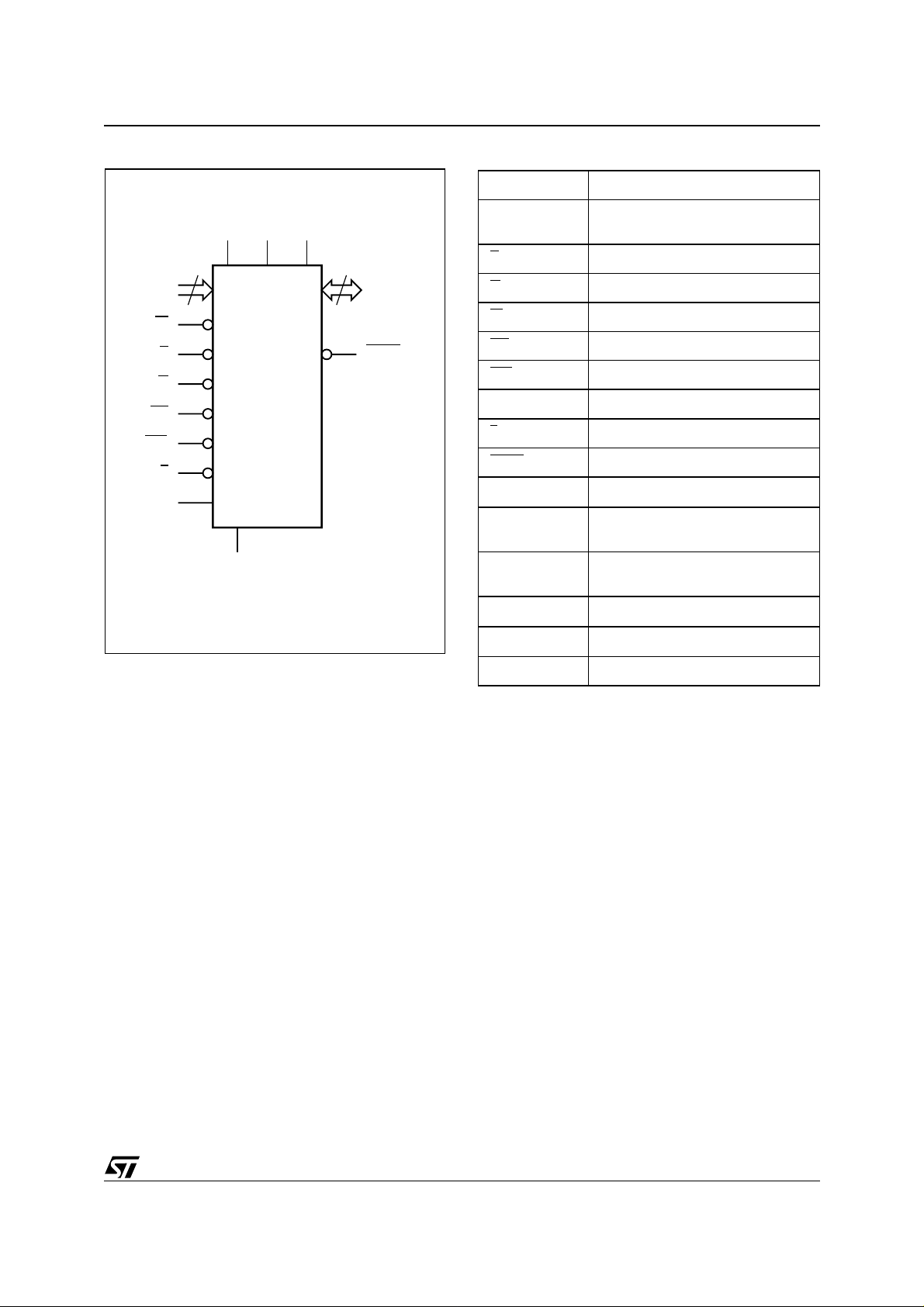
Figure 2. Logic Diagram Table 1. Signal Names
A0-A20 Address Inputs
A0-A20
W
RP
WP
DQ0-DQ15
E
G
21
V
DD
V
DDQVPP
16
DQ0-DQ15
W
E
G
M58CR032C
M58CR032D
WAIT
RP
WP
K Burst Clock
L
L
K
V
SS
AI90067
WAIT
V
DD
V
DDQ
V
PP
V
SS
V
SSQ
Data Input/Outputs or Address
Inputs, Command Inputs
Chip Enable
Output Enable
Write Enable
Reset/Power-down
Write Protect
Latch Enable
Wait Data in Burst Mode
Supply Voltage
Supply Voltage for Input/Output
Buffers
Optional Supply Voltage for
Fast Program & Erase
Ground
Ground Input/Output Supply
NC Not Connected Internally
7/63
Page 8
M58CR032C, M58CR032D
Figure 3. TFBGA Connections (Top view through package)
87654321
A6
A5A17
A7A19
NC
DQ8
V
A4
A3
SSQ
DQ1
V
A18
DDQ
A
B
C A2
D A1
E
F
G
A13
A15
V
DDQ
V
SS
DQ7 V
A8A11
A9A12
A10
A14 WAIT A16 WP
DQ15
DQ14 DQ11 DQ10 DQ9 DQ0 G
SSQ
V
SS
A20
NC
DQ6
DQ13
DQ5 V
V
DD
K RP
L W
DQ4 DQ2 E A0
DD
V
PP
DQ12
DQ3
AI90001
Table 2. Bank Architecture
Bank A 8 Mbit 8 blocks of 4 KWord 15 blocks of 32 KWord
Bank B 24 Mbit - 48 blocks of 32 KWord
8/63
Bank Size Parameter Blocks Main Blocks
Page 9
Figure 4. Me m ory Map
M58CR032C, M58CR032D
Bank B
Bank A
000000h
007FFFh
178000h
17FFFFh
180000h
187FFFh
1F0000h
1F7FFFh
1F8000h
1F8FFFh
Top Boot Block
Address lines A20-A0
512 Kbit or
32 KWord
512 Kbit or
32 KWord
512 Kbit or
32 KWord
512 Kbit or
32 KWord
64 Kbit or
4 KWord
Total of 48
Main Blocks
Total of 15
Main Blocks
Total of 8
Parameter
Blocks
Bank A
Bank B
000000h
000FFFh
007000h
007FFFh
008000h
00FFFFh
078000h
07FFFFh
080000h
087FFFh
Bottom Boot Block
Address lines A20-A0
64 Kbit or
4 KWord
Total of 8
Parameter
Blocks
64 Kbit or
4 KWord
512 Kbit or
32 KWord
Total of 15
Main Blocks
512 Kbit or
32 KWord
512 Kbit or
32 KWord
Total of 48
Main Blocks
1FF000h
1FFFFFh
64 Kbit or
4 KWord
1F8000h
1FFFFFh
Figure 5. Security Block and Protection Register Memory Map
PROTECTION REGISTER
SECURITY BLOCK
Parameter Block # 0
88h
85h
84h
81h
80h
User Programmable OTP
Unique device number
Protection Register Lock 2 1 0
512 Kbit or
32 KWord
AI90069
AI90004
9/63
Page 10

M58CR032C, M58CR032D
SIGNAL DESCRIPTIONS
See Figure 2 Lo gic Diagram, and Tabl e 1, Sign al
Names, for a brief overview of the signals connected to this device.
Address Inputs (A0-A20). The Address Inputs
select the cells i n the memory array to a ccess during Bus Read operations. During Bus Write operations they control the commands sent to the
Command Interface of the internal state machine.
The address inputs for the memory array are
latched on the rising edge of Latch E nable L
address latch is transparent when L
is at VIL. In
synchronous operations the address is also
latched on the first rising/falling edge of K (depending on clock configuration) when L
During a Write operation the address is latched on
the rising edge of L
or W, whichever occurs first.
Data Inputs/Outputs (DQ0-DQ15). The Data Inputs/Outputs output the data stored at the selected
address during a Bus Read operation. During Bus
Write operations they represent the commands
sent to the Command Interface of the internal state
machine.
Both input data and commands are latched on the
rising edge of Write Enable, W
able, E
, and Output Enable, G, are at VIL the data
. When Chip En-
bus outputs data from the Memory Array, the Electronic Signature, Manufacturer or Device codes,
the Block Protection Status, the Burst Configuration Register, the Protection Register or the Status
Register. The data bus is high impedance when
the chip is deselected, Output Enable, G
or Reset/Power-Down, RP
Chip Enable (E
). The Chip Enable input acti-
, is at VIL.
vates the memory control logic, input buffers, decoders and sense amplifiers. When Chi p Enable,
E
, is at VIH, the memory is deselected and the
power consumption is reduced to the standby level. Chip Enable can also be used to control writing
to the Command Interface and to the mem ory array, while Write Enable, W
Output Enable (G
). The Output Enable gates the
, remains at VIL.
outputs through the data buffers during a read operation. When Output Enable, G
, is at VIH the out-
puts are high impedance.
Write Enable (W
). The Write Enable controls the
Bus Write operation of the memory’s Command
Interface. Data are latched on the rising edge of
Write Enable.
Write Protect (WP
). Write Protect is an input that
gives an additional hardware protection for each
block. When Write Protect is at V
, the Lock-Down
IL
is enabled and the protection status of the block
cannot be changed. When Write Protect is at V
the Lock-Down is disabled and the block can be
locked or unlocked. (refer to Table 10, Read Protection Register).
. The
is low.
, is at VIH,
IH
Reset/Power-Down (RP
). The Reset/Power-
Down input provides hardware reset of the memory, and/or Power-Down functions, depending on
the Burst Configuration Register status. A Reset or
Power-Down of the memory is achieved by pulling
RP
to VIL for at least t
. When the reset pulse
PLPH
is given, the memory will recover from PowerDown (when enabled) in a minimum of t
t
or t
PHLL
the rising edge of RP
(see Table 25 and Figure 16) after
PHWL
. After a Reset or Power-Up
the device is configured for asynchronous page
read (M15=1) and the power save func tion is disabled (M10=0). All blocks are locked after a Reset
or Power-Down. Either Chip Enable or W rite Enable must be tied to V
during Power-Up to allow
IH
maximum security and the possibility to write a
command on the first rising edge of Write Enable.
Latch Enable (L
). Latch Enable l atches t he ad-
dress bits A0-A20 on its rising edge. The address latch is transparent when L
it is inhibited when L
is at VIH.
is a t VIL and
Clo c k (K). The clock input synchronizes the
memory to the microcontroller during burst mode
read operation; the address is latched on a K edge
(rising or falling, according to the configuration settings) when L
is at VIL. K is don't care during asyn-
chronous page mode read and in write operations.
Wait (WAIT
). Wait is an output signal used during
burst mode read, indicating whether the data on
the output bus are valid or a wait state must be inserted. This output is high impedance when C hip
Enable or Output Enable are at V
er-Down is at V
. It can be configured to be active
IL
or Reset/Pow-
IH
during the wait cycle or one clock cycle in advance.
Supply Voltage (1.65V to 2V). V
V
DD
vides the power supply to the internal core of the
memory device. It is the main power supply for all
operations (Read, Program and Erase). It ranges
from 1.65V to 2.0V.
Supply Voltage (1.65V to 3.3V). V
V
DDQ
provides the power supply to the I/O pins and enables all Outputs to be powered independently
from V
DD
. V
can be tied to VDD or it can use a
DDQ
separate supply. It can be powered either from
1.65V to 2.0V or from 1.65V to 3.3V.
V
Program Supply Voltage (12V).
PP
is a power supply pin. The Supply Voltage
V
PP
and the Program Supply Voltage VPP can be
V
DD
applied in any order. The pin can also be used as
a control input.
The two functions are selected by the voltage
range applied to the pin. If V
,
age range (0V to 2V) V
is kept in a low volt-
PP
is seen as a control in-
PP
put. In this case a voltage lower than V
an absolute protection against program or era se,
DD
PPLK
DDQ
gives
PHEL
pro-
,
10/63
Page 11

M58CR032C, M58CR032D
while VPP > V
enables these functions (see Ta-
PP1
ble 19, DC Characteristics for the relevant values).
V
is only sampled at the beginning of a program
PP
or erase; a change in its value after the operation
has started does not have any effect on Program
or Erase, however for Double or Quadruple Word
Program the results are uncertain.
is in the range 11.4V to 12.6V it acts as a
If V
PP
power supply pin. In this condition V
must be
PP
stable until the Program/Erase algorit hm is completed (see Table 16 and 17). In read mode the
current sunk is less then 0.5mA, while during pro-
gram and erase operations the current may increase up to 10mA.
V
and V
SS
Grounds. VSS and V
SSQ
SSQ
grounds
are the reference for the core supply and the input/
output voltage measurements respectively.
Note: Each device in a system should have
V
DD, VDDQ
and VPP decoupled wi th a 0.1 µF ca-
pacitor close to the pin. See Figure 10, AC Measurement Load Circu it. The PCB trace widths
should be sufficient to carry the required V
PP
program and erase currents.
11/63
Page 12

M58CR032C, M58CR032D
BUS OPERATIONS
There are two types of bus operations that control
the device: Asynchronous (Read, Page Read,
Write, Output Disable, Standby, Automatic Standby and Reset/Power-Down) and Synchronous
(Synchronous Read and Synchronous Burst
Read).
The Dual Bank architecture of the M58CR032 allows read/write operations in Bank A, while read
operations are being executed in Bank B or vice
versa. Write operations are only allowed in one
bank at a time (see Table 7).
See Table 3, Bus Operations, for a summary. Typically glitches of less than 5ns on Chip Enab le or
Write Enable are ignored by the memory and do
not affect bus operations.
Asynchronous Read. Asynchronous Read operations read from the Memory Array, or specific
registers (Electronic Signature, Status Register,
CFI, Block Protection Status, Read Configuration
Register status and Protection Register) in the
Command Interface.
A valid Asynchronous Bus Read operation involves setting the desired address on the Address
Inputs, applying a Low sig nal, V
and Output Enable and keeping Write Enable
High, V
edge of the Latch, L
. The address is latched on the rising
IH
, input. The Data Inputs/Outputs will output the value, see Figure 11, Asynchronous Read AC Waveforms, and Table 21,
Asynchronous Read AC Characteristics, for details of when the output becomes valid.
According to the device configuration the following
Read operations: Electronic Signature, Status
Register, CFI, Block Protection Status, Burst Configuration Register Status and Protection Register
must be accessed as asynchronous read or as
single synchronous read.
Asynchronous Page Read. Asynchronous
Page Read operations can be used to read the
content of the memory array, where data is internally read and stored in a page buffer. The page
has a size of 4 words and is addressed by A0 and
A1 address inputs.
Valid bus operations are the same as Asynchronous Bus Read operations but with different timings. The first read operation within the page has
identical timings, subsequent reads within the
same page have much sh orter access t i mes. If the
page changes then the normal, longer timings apply again. See Figure 12, Asynchronous Page
Read AC Waveforms and Table 21, Asynchronous Read AC Characteristics for details on when
the outputs become valid.
Asynchronous Page Read is the default st ate of
the device when exiting power-down or after power-up.
, to Chip Enable
IL
Asynchronous Write. Bus Write operations are
used to write to the Command Interface of the
memory or latch Input Data to be programmed. A
valid Bus Write operation begins by setting the desired address on the Address Inputs and setting
Chip Enable, E
Output Enable to V
the rising edge of L
, and Write Enable, W, to VIL and
. Addresses are latched on
IH
, W or E whichever occur first.
Commands and Input Data are latched on t he rising edge of W
Enable must remain High, V
or E whichever occurs first. Output
, during the whole
IH
Bus Write operation. See Figures 14 and 15, Write
AC Waveforms, and Tables 23 and 24, Write AC
Characteristics, for details of the timing requirements.
Write operations are asynchronous and the clock
is ignored during write.
Output Disa bl e . The data outputs are high impedance when the Output Enable, G
Enable, W
, are High, VIH.
Standby. When Chip Enable is High, V
, and Write
, and the
IH
Program/Erase Controller is idle, the m emory enters Standby mode and t he Data Inputs/Outputs
pins are placed in the high impedance state, independent of Output Enable, G
, or Write Enable, W.
For the Standby current level see T able 19, DC
Characteristics.
Reset/Power-Down. The memory is in PowerDown when the Burst Configuration Register is set
for Power-Down and RP
is at VIL. The power consumption is reduced to the Power-Down level, and
Outputs are in high impedance, independent of
Chip Enable E
W
. The memory is in reset mode when the Burst
Configuration Register is set for Reset and RP
. The power consumption is the s am e of t he
at V
IL
, Output Enabl e G or Write Ena ble
is
standby and the outputs are in hig h impedance.
After a Reset/Power-Down the de vice defaults to
Asynchronous Page Read, the Status Register is
cleared and the Burst configuration register defaults to Asynchronous Page read.
Automatic Standby. If CMOS levels (V
DD
±
0.2V) are used to drive the b us and the bu s is inactive for 150ns or more in Read mode, the memory enters Automatic Standby where the internal
Supply Current is reduced to the Standby Supply
Current, I
. The Data Inputs/Outputs will still
DD2
output data if a Bus Read operation is in progress.
The automatic standby feature is not available
when the device is configured for synchronous
burst mode.
Synchronous Single Read. Synchronous single Reads can be used to read the Electronic Signature, Status Register, CFI, Block Protection
Status, Burst Configuration Register Status or
12/63
Page 13
M58CR032C, M58CR032D
Protection Register, see F igure 6, for an example
of a single synchronous read operation.
Synchronous Burst Read. The device also supports a synchronous burst read. In this mode a
burst sequence is started at the f irst clock edge
(rising or falling according to configuration settings) after the falling edge o f La tch Enable. After
a configurable delay of 2 to 5 clock c ycles a new
data is output at e ach clock cycle. The burst sequence may be configured t o be sequent ial or interleaved and for a length of 4 or 8 words or for
continuous burst mode (s ee Table 5, Burst Type
Definition). Wrap and no-wrap modes are also
supported.
A WAIT
system that an output delay will occur. This delay
will depend on the starting address of the burst sequence; the worst case dela y will o ccur w hen the
sequence is crossing a 64 word boundary and the
starting address was at the end of a four word
boundary. See the Burst Configuration Register
command for more details on all the possible settings for the synchronous burst read (see Table 4).
It is possible to perform burst read across bank
boundaries (all banks in read array mode).
Table 3. Bus Operations
Operation E G W L KRPWP DQ15-DQ0
Asynchronous Read
Asynchronous Page Read
Asynchronous Write
Output Disable
Standby
V
IL
V
IL
V
IL
V
IL
V
IH
V
IL
V
IL
V
IH
V
IH
V
IH V
V
IH
V
IL
V
IH
XXXX
Reset / Power-Down X X X X X
Synchronous Read
Synchronous Burst Read
Note: 1. X = Don’t care.
2. T = transition, falling edge for L
is started on the first active clock edge after the falling edge of Latch Enable.
3. L
can be tied to VIH if the valid address has been previously latched
V
IL
V
IL
, rising or falling edge for K depending on M6 in the Burst Configu ration Register. The burst sequence
V
IL
V
IL
V
IH
V
IH
(3)
IL
(3)
V
IL
(3)
V
IL
XX
(2)
T
(2)
T
signal may be asserted to indicate to the
X
X
X
(2)
T
(2)
T
V
IH
V
IH
V
IH
V
IH
V
IH
V
IL
V
IH
V
IH
X Data Output
X Data Output
V
IH
V
IH
Data Input
Hi-Z
X Hi-Z
X Hi-Z
X Data Output
X Data Output
13/63
Page 14
M58CR032C, M58CR032D
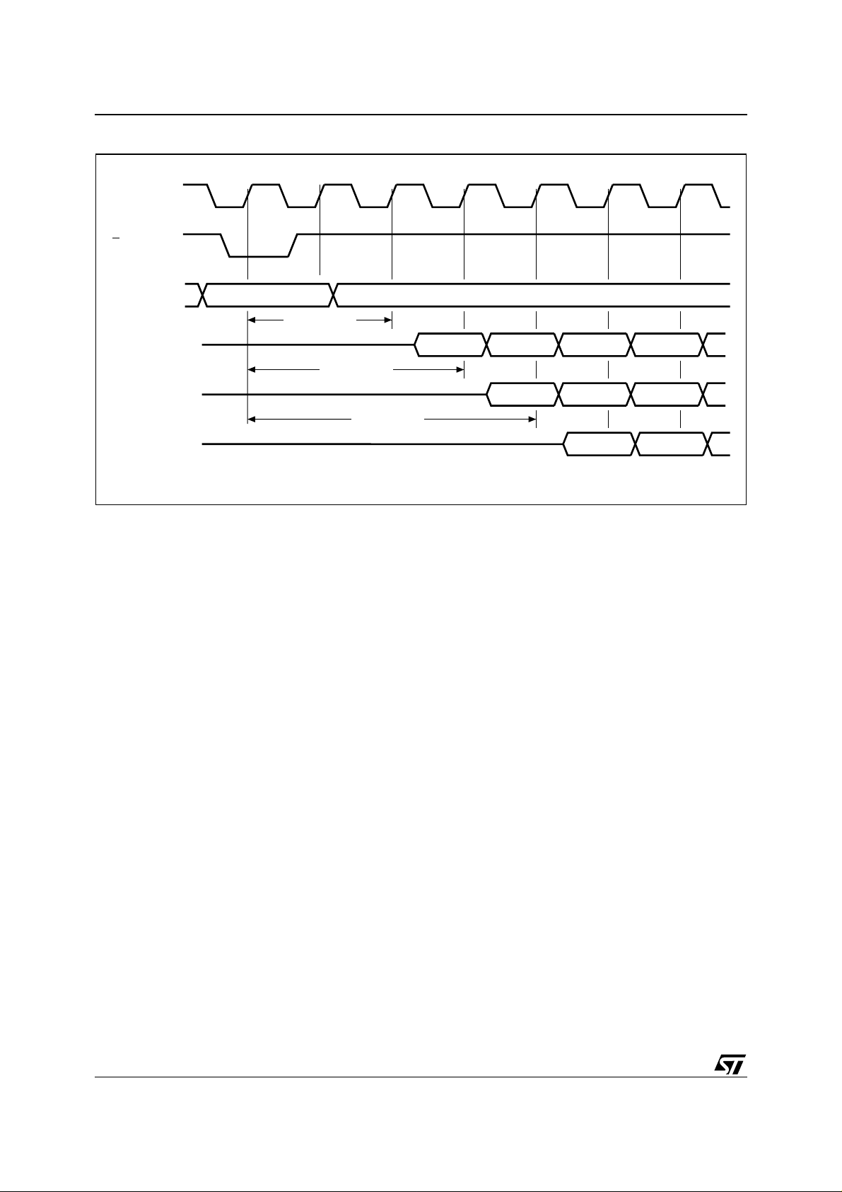
Figure 6. Synchronous Single Read Operation
K
L
A20-A0
DQ15-DQ0
DQ15-DQ0
DQ15-DQ0
VALID ADDRESS
X latency = 2
X latency = 3
X latency = 4
VALID DATA NOT VALID
VALID DATA
NOT VALID
NOT VALID
VALID DATA
NOT VALID
NOT VALID
NOT VALID
AI90103
14/63
Page 15

M58CR032C, M58CR032D
Burst Configuration Register
The Burst Configuration Register is used to configure the type of bus access that the memory will
perform.
The Burst Configuration Register is set through
the Command Interface. After a Reset or PowerUp the device is configured for asynchronous
page read (M15 = 1) and the power sav e func tion
is disabled (M10 = 0). The Burst Configuration
Register bits are described in Table 4. They specify the selection of the burst length, burst type,
burst X latency and the Read operation. Refer to
Figures 7 and 8 for examples of synchronous burst
configurations.
Read Select Bit (M15). The Read Select bit,
M15, is used to switch between asynchronous and
synchronous Bus Read operations. When the
Read Select bit is set to ’1’, Bus Read operations
are asynchronous; when the Read Select but is
set to ’0’, Bus Read operations are synchronou s.
Synchronous Burst Read is supported in both parameter and main blocks and can be performed
across banks.
On reset or power-up the Read Sel ect bit is set
to’1’ for asynchronous access.
X-Latency Bits (M13-M11). The X-Latency bits
are used during Synchronous Bus Read operations to set the n umber of clock cycl es between
the address being latched and the first data becoming available. For correct operation the X-Latency bits can only assume the values in Table 4,
Burst Configuration Register.
The correspondence be tween X-Latency settings
and the maximum sustainable freq uency must be
calculated taking into account some system parameters.
Two conditions must be satisfied:
–(n + 1) t
–tK > t
KQV
K
+ t
- t
ACC
AVK_CPU
QVK_CPU
+ t
QVK_CPU
≥ t
where "n" is the chosen X-Latency configuration
code, t
is the clock period, t
K
Address Valid, L
last, and t
QVK_CPU
Low or E Low, whichever occurs
AVK_CPU
is the data setup t ime required
is Cloc k to
by the system CPU.
Power-Down Bit (M10). The Power-Down bit is
used to enable or disable the power-down function. When the Power-Down bit is set to ‘0’ (default) the power-down func tion is disabled. W hen
the Power-Down bit is set to ‘1’ power-down is enabled and the device goes into the power-down
state where the I
typical figure of I
supply current is reduced to a
DD
.
DD2
if this function is disabled the Reset/Power-Down,
RP
, pin causes o nly a reset of the dev i ce and the
supply current is the standby value. The recovery
time after a Reset/Power-Down, RP
, pulse is sig-
nificantly longer when power-down is enabled
(see Table 25).
Wait Bit (M8). In burst mode the Wait bit controls
the timing of the Wait output pin, WAIT
. When the
Wait bit is ’0’ the Wait output pin is asserted during
the wait state. When the Wait bit is ’1’ (default) the
Wait output pin is asserted one clock cycle before
the wait state.
WAIT
is asserted during a continuous burst and
also during a 4 or 8 burst length if no-wrap configuration is selected. WAIT
is not asserted during
asynchronous reads, single synchronous reads or
during latency in synchronous reads.
Burst Type Bit ( M7 ). The Burst Type bit is used
to configure the sequence of addresses read as
sequential or interleaved. When the Burst Type bit
is ’0’ the memory outputs from interleaved addresses; when the Burst Type bit is ’1’ (default) the
memory outputs from sequential addresses. See
Tables 5, Burst Type Definition, for the seq uence
of addresses output from a given starting address
in each mode.
Valid Clock Edge Bit (M6). The Valid Clock
Edge bit, M6, is used to configu re the active e dge
of the Clock, K, during Synchronous Burst Read
operations. When the Valid Clock Edge bit is ’0’
the falling edge of the Clock is the active edge;
when the Valid Clock Edge bit is ’1’ the rising edge
of the Clock is active.
Wrap Burst Bit (M3). The burst reads can be
confined inside the 4 or 8 Double-Word boundary
(wrap) or overcome the boundary (no wrap). The
Wrap Burst bit is used to select between wrap and
no wrap. When the Wrap Burst bit is set to ‘0’ the
burst read wraps; when it is set to ‘1’ the burst read
does not wrap.
Burst length Bits (M2-M0). The Burst Length
bits set the number of Words to be output during a
Synchronous Burst Read operation; 4 words, 8
words or continuous burst, where all the words are
read sequentially.
In continuous burst mode the burs t sequ ence c an
cross bank boundaries.
In continuous burst mode or in 4, 8 words no-wrap,
depending on the starting add ress, the dev ice activates the WAIT
output to indicate that a delay is
necessary before the data is output.
If the starting address is aligned to a 4 word
boundary no wait states are needed and the WAIT
output is not activated.
If the starting address is shifted by 1,2 or 3 positions from the four word boundary, WAIT
will b e
asserted for 1, 2 or 3 clock cycles when the burst
sequence crosses the first 64 word b oundary, to
indicate that the device needs an internal delay to
read the successive words in the array. WAIT
will
15/63
Page 16
M58CR032C, M58CR032D
be asserted only once during a continuous burst
access. See also Table 5, Burst Type Definition.
Table 4. Burst Configuration Registe r
Bit Description Value Description
M15 Read Select
M14 Reserved
M13-M11
M10
M9 Reserved
M8 Wait
X-Latency
Power-Down
(2)
(3)
0 Synchronous Burst Read
1 Asynchronous Page Read (Default at power-on)
010 2 clock latency
011 3 clock latency
100 4 clock latency
101 5 clock latency
111 Reserved
Other configurations reserved
0 Power-Down disabled
1 Power-Down enabled
0 WAIT
1 WAIT
M14, M9 , M5 and M4 are reserved for future use.
is active during wait state
is active one data cycle before wait state (default)
M7 Burst Type
M6 Valid Clock Edge
M5-M4 Reserved
M3 Wrapping
M2-M0 Burst Length
0 Interleaved
1 Sequential (default)
0 Falling Burst Clock edge
1 Rising Burst Clock edge
0 Wrap
1 No wrap
001 4 words
010 8 words
111 Continuous (M7 must be set to ‘1’)
16/63
Page 17
Tabl e 5. Burst Type Definition
Start
Address 4 Words 8 Words
Mode
Sequential Interleaved Sequential Interleaved
0 0-1-2-3 0-1-2-3 0-1-2-3-4-5-6-7 0-1-2-3-4-5-6-7 0-1-2-3-4-5-6...
1 1-2-3-0 1-0-3-2 1-2-3-4-5-6-7-0 1-0-3-2-5-4-7-6 1-2-3-4-5-6-7...
2 2-3-0-1 2-3-0-1 2-3-4-5-6-7-0-1 2-3-0-1-6-7-4-5 2-3-4-5-6-7-8...
3 3-0-1-2 3-2-1-0 3-4-5-6-7-0-1-2 3-2-1-0-7-6-5-4 3-4-5-6-7-8-9...
...
7 7-4-5-6 7-6-5-4 7-0-1-2-3-4-5-6 7-6-5-4-3-2-1-0 7-8-9-10-11-12-13...
Wrap
...
60 60-61-62-63-64-65-66...
61 61-62-63-WAIT-64-65-66...
62 62-63-WAIT-WAIT-64-65-66...
63
Sequential Interleaved Sequential Interleaved
0 0-1-2-3 0-1-2-3-4-5-6-7 0-1-2-3-4-5-6...
M58CR032C, M58CR032D
Continuous Burst
63-WAIT-WAIT-WAIT-64-65-
66...
1 1-2-3-4 1-2-3-4-5-6-7-8 1-2-3-4-5-6-7...
2 2-3-4-5 2-3-4-5-6-7-8-9... 2-3-4-5-6-7-8...
3 3-4-5-6 3-4-5-6-7-8-9-10 3-4-5-6-7-8-9...
...
7 7-8-9-10 7-8-9-10-11-12-13-14 7-8-9-10-11-12-13...
...
No-wrap
60 60-61-62-63
61 61-62-63-WAIT-64
62
63
62-63-WAIT-
WAIT-64-65
63-WAIT-WAITWAIT-64-65-66
60-61-62-63-64-65-66-
67
61-62-63-WAIT-64-65-
66-67-68
62-63-WAIT-WAIT-64-
65-66-67-68-69
63-WAIT-WAIT-WAIT-
64-65-66-67-68-69-70
60-61-62-63-64-65-66...
61-62-63-WAIT-64-65-66...
62-63-WAIT-WAIT-64-65-66...
63-WAIT-WAIT-WAIT-64-65-
66...
17/63
Page 18
M58CR032C, M58CR032D
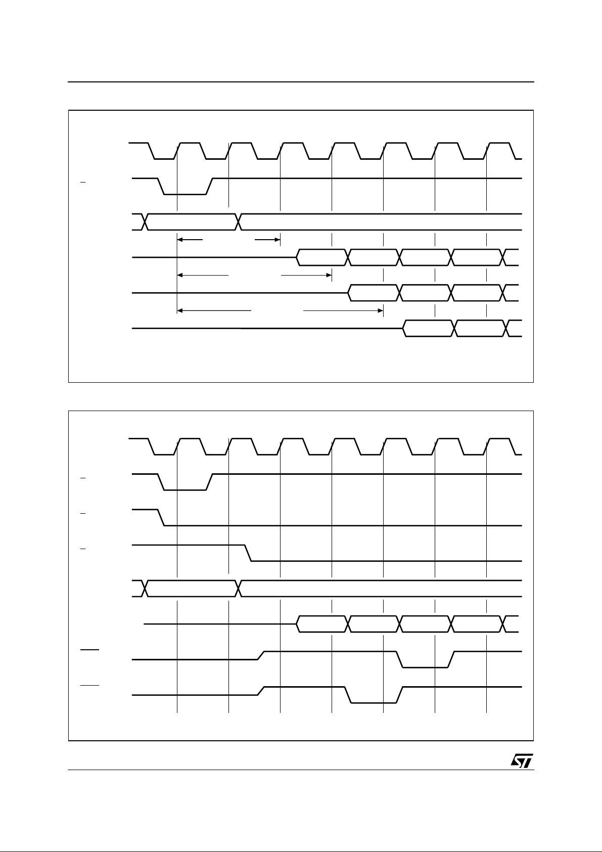
Figure 7. X-L at ency Configu ra tion Sequence
K
L
A20-A0
DQ15-DQ0
DQ15-DQ0
DQ15-DQ0
VALID ADDRESS
X latency = 2
X latency = 3
Figure 8. Wai t Co nf i gu ra tio n Sequence
K
L
X latency = 4
VALID DATA VALID DATA
VALID DATA
VALID DATA
VALID DATA
VALID DATA
VALID DATA
VALID DATA
VALID DATA
AI90105
E
G
A20-A0
DQ15-DQ0
WAIT
M8 = '0'
WAIT
M8 = '1'
18/63
VALID ADDRESS
VALID DATA
VALID DATA NOT VALID VALID DATA
AI90106
Page 19

COMMAND INTERFACE
All Bus Write operations t o the me mory are in terpreted by the Command Interface. Commands
consist of one or more sequential Bus Write operations. An internal Program/Erase Controller handles all timings and verifies the correct execution
of the Program and Erase commands. The Program/Erase Controller provides a S tatus Register
whose output may be read at any time during, to
monitor the progress of the operation, or the P rogram/Erase states. See Appendix C, Tables 36
and 37, Command Interface States - Lock and
Modify Tables, for a summary of the Command Interface.
The Command Interface is reset to Read mode
when power is first applied, when exiting from Reset or whenever V
is lower than V
DD
LKO
. Command sequences must be followed exactly. Any
invalid combination of commands will reset the device to Read mode. Refer to Table 6, Commands,
in conjunction with the text descriptions below.
Read Command.
The Read command returns the addressed bank
to Read mode. One Bus Write cycle is required to
issue the Read command and return the addressed Bank to Read mode. Subsequent read
operations will read the addressed location and
output the data. A Read com mand can be issued
in one bank while programming or era sing in the
other bank. However if a Read command is issued
to a bank currently executing a program or erase
operation the command will be ignored.
When a device Reset occurs, the memory defaults
to Read mode.
Read Status Register Command
A bank’s Status Register indicates when a program or erase operation is complete and the success or failure of operation itself. Issue a Read
Status Register command to read the Status Register content of the addressed bank. The status of
the other bank is not affected by the command.
The Read Status Register command can be issued at any time, eve n during program or erase
operations.
The following Read operations output the content
of the Status Register of the addressed bank. The
Status Register is latched on the falling edge of E
or G signals, and can be read until E or G returns
to V
. Either E or G must be toggled to update the
IH
latched data. See Table 1 5 for the description of
the Status Register Bits. This mode supports
asynchronous or single synchronous reads only.
Read Electronic Signature Command
The Read Electronic Signature command reads
the Manufacturer and Device Codes and the Block
Locking Status, or the Protection Register.
M58CR032C, M58CR032D
The Read Electronic Signature command consists
of one write cycle to an address within the bot tom
bank. A subsequent read operation in the address
of the bottom bank will output the Manufacturer
Code, the Device Code, the protection Status of
Blocks of the bottom bank, the Die Revision Code,
the Protection Register, or the Read Configuration
Register (see Table 11).
If the first write cycle of Read Electronic Signature
command is issued t o an address within the top
bank, a subsequent read operat ion in an address
of the top bank will output the protection Statu s of
blocks of the top bank. The status of the other
bank is not affected by the command (see Ta ble
7). This mode supports asynchronous or single
synchronous reads only.
See Tables 8, 9, 10 and 11 for the valid addresses.
Read CFI Query Command
The Read CFI Query Command is used to read
data from the Common Flash Interface (CFI)
Memory Area, located in the bottom bank. One
Bus Write cycle, addressed to the bottom bank, is
required to issue the Read Query Command.
Once the command is issued subsequent Bus
Read operations in the bottom bank read from the
Common Flash Interface Mem ory Area. The status of the top bank is not affected by the command
(see Table 7). After issuing a Read CFI Query
command, a Read com mand should be issued to
return the bank to read mode.
See Appendix B, Common Flash Interface, Tables
29, 30, 31, 32, 33, 34 and 35 for detail s on the information contained in the Commo n Flash Interface memory area.
Clear Status Register Command
The Clear Status Register comm and c an b e us ed
to reset (set to ‘0’) bits 1, 3, 4 and 5 in the Status
Register of the addressed bank’. One bus write cycle is required to issue the Clear S tatus Register
command. After the Clear Status Register command the bank returns to read mode.
The bits in the Status Register do not automatically return to ‘0’ when a new Program or Erase command is issued. The error bits in the Status
Register should be cleared before attempting a
new Program or Erase command.
Block Erase Command
The Block Erase com mand can be used to erase
a block. It sets all the bits within the selected block
to ’1’. All previous d ata in th e block is lost. If th e
block is protected then the Erase operation will
abort, the data in the block will not be changed and
the Status Register will output the error. It is not
necessary to pre-program the block as the Pro-
19/63
Page 20

M58CR032C, M58CR032D
gram/Erase Controller does it automatically before
erasing.
Two Bus Write cycles are required to issue the
command.
■ The first bus cycle sets up the Erase command.
■ The second latches the block address in the
internal state machine and starts the Program/
Erase Controller.
If the second bus cycle is not Write Erase Confirm
(D0h), Status Register bits b4 and b5 a re s et and
the command aborts. E rase aborts if Re set turns
to V
. As data integrity cannot be guaranteed
IL
when the Erase operation is aborted, the block
mus t be erased again.
Once the command is issued the device outputs
the Status Register data when any address within
the bank is read. At the end o f the operation the
bank will remain in Read Status Register until a
Read command is issued.
During Erase operations the bank containing the
block being erased will onl y ac cept the Read Status Register command and the Program/Erase
Suspend command, all other commands will be ignored. Typical Erase times are given in Table 12,
Program, Erase Times and Program/Erase Endurance Cycles.
See Appendix B, Figure 22, Block Erase Flowchart
and Pseudo Code, for a suggested flowchart for
using the Block Erase command.
Bank Erase Command
The Bank Erase command can be used to erase a
bank. It sets all the bits within the selected bank to
’1’. All previous data in th e ban k is lo st. Th e B ank
Erase command will igno re any protected blocks
within the bank. If the bank is protected t hen the
Erase operation will abort, the data in the bank will
not be changed and the Status Register will output
the error.
Two Bus Write cycles are required to issue the
command.
■ The first bus cycle sets up the Bank Erase
command.
■ The second latches the bank address in the
internal state machine and starts the Program/
Erase Controller.
If the second bus cycle is not Write Bank Erase
Confirm (D0h), Status Register bits b4 and b5 are
set and the command aborts. Erase aborts if Reset tur ns to V
. As data integrity cannot be guar-
IL
anteed when the Erase operation is aborted, the
bank must be erased again.
Once the command is issued the device outputs
the Status Register data when any address within
the bank is read. At the end o f the operation the
bank will remain in Read Status Register until a
Read command is issued.
During Erase operations the bank being erased
will only accept the Read Status Register command and the Program/Erase Suspend command,
all other commands will be ignored. Typical Erase
times are given in Table 12, Program, Erase
Times and Program/Erase Endurance Cycles.
Program Command
The memory array can be programmed word-byword. Only one bank can be programmed at any
one time. The other bank must be in Re ad mode
or Erase Suspend. Two bus write cycles are required to issue the Program Command.
■ The first bus cycle sets up the Program
command.
■ The second latches the Address and the Data to
be written and starts the Program/Erase
Controller.
After programming has started, Read operations
in the bank being programmed ou tput the Status
Register content.
During Program operations the bank being programmed will only accept the Read Status Register command and the Program/Erase Suspend
command. Typical Program times are given in Table 12, Program, Erase Times and Program/Erase
Endurance Cycles.
Programming aborts if Reset goe s to V
. As data
IL
integrity cannot be guaranteed when the program
operation is aborted, the block containing the
memory location must be erased and reprogrammed.
See Appendix B, Figure 18, Program Flowchart
and Pseudo Code, for the f lowchart for using the
Program command.
Double Word Program Command
This feature is offered to improve the programming
throughput, writing a page of two adjacent words
in parallel. The two words must differ only for the
address A0. Only one bank can be programmed at
any one time. The other bank must be in Read
mode or Erase Suspend.
Programming should not be attempted when V
is not at V
is below V
V
PP
. The command can be executed if
PPH
but the result is not guaranteed.
PPH
PP
Three bus write cycles are necessary to issue the
Double Word Program command.
■ The first bus cycle sets up the Double Word
Program Command.
■ The second bus cycle latches the Address and
the Data of the first word to be written.
■ The third bus cycle latches the Address and the
Data of the second word to be written and starts
the Program/Erase Controller.
20/63
Page 21

M58CR032C, M58CR032D
Read operations in the bank bei ng programmed
output the Status Register content after the programming has started.
During Double Word Program operations the bank
being programmed will only a ccept the Read Status Register command and the Program/Erase
Suspend command. Typical Program times are
given in Table 12, Program, Erase Times and Program/Erase Endurance Cycles.
Programming aborts if Reset goe s to V
. As data
IL
integrity cannot be guaranteed when the program
operation is aborted, the block containing the
memory location must be erased and reprogrammed.
See Appendix B, Figure 19, Double Word Program
Flowchart and Pseudo Code, for the flowc hart for
using the Double Word Program command.
Quadruple Word Program Command
This feature is offered to improve the programming
throughput, writing a page of four adjacent words
in parallel. The four words must differ only for the
addresses A0 and A1. The first write cycle must be
addressed to the bank to be programmed.
Only one bank can be programmed at any one
time. The other b ank must be in Read mode or
Erase Suspend.
Programming should not be attempted when V
is not at V
V
is below V
PP
. The command can be executed if
PPH
but the result is not guaranteed.
PPH
PP
Five bus write cycles are necessary to issue the
Quadruple Word Program command.
■ The first bus cycle sets up the Double Word
Program Command.
■ The second bus cycle latches the Address and
the Data of the first word to be written.
■ The third bus cycle latches the Address and the
Data of the second word to be written.
■ The fourth bus cycle latches the Address and
the Data of the third word to be written.
■ The fifth bus cycl e latches the Address and the
Data of the fourth word to be written and starts
the Program/Erase Controller.
Read operations to the bank being programmed
output the Status Register content after the programming has started.
Programming aborts if Reset goe s to V
. As data
IL
integrity cannot be guaranteed when the program
operation is aborted, the block containing the
memory location must be erased and reprogrammed.
During Quadruple Word Program operations the
bank being programmed will only accept the Read
Status Register command and the Program/Erase
Suspend command. Typical Program times are
given in Table 12, Program, Erase Times and Program/Erase Endurance Cycles.
See Appendix B, Figure 20, Quadruple Word Program Flowchart and Pseudo Code, for the flowchart for using the Quadruple Word Program
command.
Program/Erase Suspend Command
The Program/Erase Suspend command is used to
pause a Program or Erase operation. One bus
write cycle is required to issue the Program/Erase
command and pau se the Prog ram/Erase controller. The command must be addressed to the bank
containing the program or erase operation.
During Program/Erase Suspend the Command Interface will accept the Program/Erase Resume,
Read, Read Status Register, Read Electronic Signature and Read CFI Query commands. Additionally, if the suspend operation was Erase then the
Program, Block Lock, Block Lock-Down or Protection Program commands will also be accepted.
The block being erased may be protected by issuing the Block Lock, Block Lock-Down or Protection
Program commands. Only the blocks not being
erased may be read or programmed correctly.
When the Program/Erase Resume command is issued the operation will complete.
During a Program/Erase Suspend, the device can
be placed in a pseudo-standby mode by taking
Chip Ena ble to V
Reset turns to V
. Program/Erase is aborted if
IH
.
IL
See Appendix B, Fi gure 21, Program Suspend &
Resume Flowchart and Pseudo Code, and Figure
23, Erase Suspend & Resume Flowchart and
Pseudo Code for flowcharts for using the Program/
Erase Suspend command.
Program/Erase Resu me Command
The Program/Erase Resume command can be
used to restart the Program/Erase Controller after
a Program/Erase Suspen d command has paused
it. One Bus Write cycle is required to issue the
command. The command m ust be addressed to
the bank containing the program or erase operation. Once the command is issued subsequent
Bus Read operations read the Status Register.
If a Program command is issued d uring a Block
Erase Suspend, then the erase cannot be resumed until the programming operation has completed. It is possible to accumulate suspend
operations. For example: su spend an erase operation, start a programming operation, suspend the
programming operation then read the array. See
Appendix B, Figure 21, Program Suspend & Resume Flowchart and Pseudo Code, and Figure 23,
Erase Suspend & Resume Flowchart and Pseudo
Code for flowcharts for using the Program/Erase
Resume command.
21/63
Page 22

M58CR032C, M58CR032D
Protection Regi ster Program Comm and
The Protection Register Program command is
used to Program the 64 bit user One-Time-Programmable (OTP) segment of the Protection Register. The segment is programmed 16 bits at a
time. When shipped all bits in the segment are set
to ‘1’. The user can only program the bits to ‘0’.
Two write cycles are required to issue the Protec-
tion Register Program command.
■ The first bus cycle sets up the Protection
Register Program command.
■ The second latches the Address and the Data to
be written to the Protection Register and starts
the Program/Erase Controller.
Read operations output the Status Register content after the programming has started.
The segment can be protected by programming bit
1 of the Protection Lock Register. Bit 1 of the P rotection Lock Register prote cts bit 2 of the P rotection Lock Register. Programming bit 2 of the
Protection Lock Register will result in a permanent
protection of the Security Block (see Figure 5, Security Block and Protection Register Memory
Map). Attempting to program a previously protected Protection Register will result in a Status Register error. The protection of the Protection
Register and/or the Security Block is not reversible.
The Protection Register Program cannot be suspended. See Appendix B, Figure 25, Protection
Register Program Flowchart and Pseudo Code,
for a flowchart for using the Protection Register
Program command.
Block Lock Command
The Block Lock command is used to lock a block
and prevent Program or Erase operations from
changing the data in it. All blocks are locked at
power-up or reset.
Two Bus Write cycles are required to issue the
Block Lock command.
■ The first bus cycle sets up the Block Lock
command.
■ The second Bus Write cycle latc hes the block
address.
The lock status can be monitored for each block
using the Read Electronic Signature command.
Table. 14 shows the Lock Status after issuing a
Block Lock command.
The Block Lock bits are vo latile, once set they remain set until a hardware reset or power-down/
power-up. They are cleared by a Blocks Unlock
command. Refer to the section, Block Locking, for
a detailed explanation. See Appendix B, Figure
24, Locking Operations Flowchart and Pseudo
Code, for a flowchart for using the Lock command.
Block Unlock Command
The Blocks Unlock command i s used to unlock a
block, allowing the block to be programmed or
erased. Two Bus Write cycles are requ ired to issue the Blocks Unlock command.
■ The first bus cycle sets up the Block Unlock
command.
■ The second Bus Write cycle latc hes the block
address.
The lock status can be monitored for each block
using the Read Electronic Signature command.
Table. 13 shows the protection status after issuing
a Block Unlock command. Refer to the section,
Block Locking, for a detailed expla nation and A ppendix B, Figure 24, Locking Operations Flowchart and Pseudo Code, f or a flowchart for using
the Unlock command.
Block Lock-Down Command
A locked block cannot be Programmed or Erased,
or have its protection status changed when WP
low, V
. When WP is high, V
IL
the Lock-Down
IH,
is
function is disabled and the locked blocks can be
individually unlocked by the Block Unlock command.
Two Bus Write cycles are required to issue the
Block Lock-Down command.
■ The first bus cycle sets up the Block Lock
command.
■ The second Bus Write cycle latc hes the block
address.
The lock status can be monitored for each block
using the Read Electronic Signature command.
Locked-Down blocks revert to the locked (and not
locked-down) state when the device is reset on
power-down. Table. 14 shows the Lo ck Statu s after issuing a Block Lock-Down command. Refer to
the section, Block Locking, for a detailed explanation and Appendix B, Figure 24, Locking Operations Flowchart and Pseudo Code, for a flowchart
for using the Lock-Down command.
Set Burst Configuration Register Command.
The Set Burst Configuration Register command is
used to write a new value t o the Burst Conf iguration Control Register which defines the burst
length, type, X latency, Synchronous/Asynchronous Read mode and the valid Clock edge configuration.
Two Bus Writ e cycles a re required to i ssue the Set
Burst Configuration Register command. The first
cycle writes the setup command and the address
corresponding to the Set Burst Configuration Register content. The second cycle writes the Burst
Configuration Register data and the confirm command. Once the command is issued the memory
returns to Read mode as if a Read Memory Array
command had been issued.
22/63
Page 23

The value for the Burst Configuration Register is
always presented on A0-A15. M0 is on A0, M1 on
A1, etc.; the other address bits are ignored.
Table 6. Commands
M58CR032C, M58CR032D
Bus Write Operations
Commands
Read Memory
Array
Read Status
Register
Read Electronic
Signature
Read CFI Query 1+ Write QA 98h Read QA QD
Block Erase 2 Write BA 20h Write BA D0h
Bank Erase 2 Write BKA 80h Write BKA D0h
Program 2 Write PA
Double Word
Program
Quadruple Word
Program
Clear Status
Register
Program/Erase
Suspend
Program/Erase
Resume
Block Loc k 2 Write BA 60h Write
Block Unlock 2 Write BA 60h Write
Block Loc k-Down 2 Write BA 60h Write
Protection
Register Program
Set Burst
Configur ation
Register
Note: 1. X = Don’t Care, RA=Read Address, RD = Read Data , SR D= St at us Re gis te r D at a, ESA= El e ct ro n ic Sig n atu r e A ddre ss , I D= Id enti f i er
(3)
(4)
(Manufac ture and De vic e Cod e), QA= Que ry Ad dres s, QD =Query D ata, BA=B loc k Add ress , PA= Progr am A d dress , P D=Pr ogram
Data, PRA=Protection Register Address, PRD=Protection Register Data, BCRA=Burst Configuration Register Address,
BCRD=Bur st Configurat i on Register Data.
2. The s i gnature addr esses are list ed in Tables 8, 9 and 10.
3. Program Addres ses 1 and 2 must be consecutive Addresses differing only for A0.
4. Program Addres ses 1,2,3 and 4 m ust be consec utive Addr esses differing only for A 0 and A1.
1+ Write BKA FFh
1+ Write BKA 70h Read BKA SRD
1+ Write ESA 90h Read
3 Write PA1 30h Write PA1 PD1 Write PA2 PD2
5 Write PA1 55h Write PA1 PD1 Write PA2 PD2 Write PA3 PD3 Write PA4 PD4
1WriteBKA 50h
1WriteBKA B0h
1WriteBKA D0h
2 Write PRA C0h Write
2 Write BCRA 60h Write
1st Cycle 2nd Cycle 3rd Cycle 4th Cycle 5th Cycle
Cycles
Op. Add Data Op. Add Data Op. Add Data Op. Add Data Op. Add Data
Read
40h
or
Write PA PD
10h
RA RD
(2)
ESA
IDh
BA 01h
D0h
BA
BA 2Fh
PRD
PRA
BCRA
03h
23/63
Page 24

M58CR032C, M58CR032D
Table 7. Dual Bank Operations
Commands allowed in the other bank
Status of one
bank
Read
Array
Read
Status
Read
CFI
Program
Idle Yes Yes Yes Yes Yes Yes Yes Yes
Reading ––––––––
Programming Yes Yes Yes – – – – Yes
Erasing Yes Yes Yes – – – – Yes
Program
Suspended
Erase
Suspended
Note: 1. For detailed description of command see Table 6, 36 and 37.
2. Ther e i s a S tatus Regi st er for each ba nk; Status Regi ster indicates bank st ate, not P/E.C. status.
3. Command must be written to a n address within the bl ock targeted by that com m and.
Yes Yes Yes – – – – Yes
Yes Yes Yes Yes – Yes – Yes
Table 8. Read Electronic Signature
Code Device E
Manufacturer Code
M58CR032C
V
IL
V
IL
Device Code
M58CR032D
Note: 1. Addresses are latched on the rising edge of L input.
2. ESA m eans Electronic Signature Addre ss (see Read Electronic Si gnature)
V
IL
G W
V
IL
V
IL
V
IL
V
IH
V
IH
V
IH
Erase/
Erase
Resume
Program
Suspend
A1 A0
V
IL
V
IL
V
IL
V
V
V
Erase
Suspend
Other
Addresses
IL
IH
IH
ESA
ESA
ESA
(2)
(2)
(2)
Lock
Unlock
DQ15-DQ0
0020h
88C8h
88C9h
Table 9. Read Block Protection
Block Status E
Locked Block
Unlocked Block
Locked and Locked-Down Block
Unlocked and Locked-Down
Note: 1. Addresses are latched on the rising edge of L input.
2. A locked block ca n onl y be unlocked with WP
3. BA means Block Address. Fir st cy cle command address should indicat e the bank of the bl ock addres s.
V
IL
V
IL
V
IL
V
IL
24/63
G W A0 A1
at V
V
IL
V
IL
V
IL
V
IL
IH.
V
IH
V
IH
V
IH
V
IH
V
IL
V
IL
V
IL
V
IL
Other
Address
V
IH
V
IH
V
IH
V
IH
BA
BA
BA
BA
(3)
(3)
(3)
(3)
DQ15-DQ0
0001
0000
0003
0002
Page 25

M58CR032C, M58CR032D
Table 10. Read Protection Register
Word E G W A20-16 A15-8 A 7-0 D Q15 -8 DQ7-3 DQ2 DQ1 D Q0
Lock
Unique ID 0
Unique ID 1
Unique ID 2
Unique ID 3
OTP 0
OTP 1
OTP 2
OTP 3
Note: 1. Addresses are latched on the rising edge of L input.
2. X = Don’t ca re.
V
ILVILVIH
V
ILVILVIH
V
ILVILVIH
V
ILVILVIH
V
ILVILVIH
V
ILVILVIH
V
ILVILVIH
V
ILVILVIH
V
ILVILVIH
X
X
X
X
X
X
X
X
X
(2)
(2)
(2)
(2)
(2)
(2)
(2)
(2)
(2)
X
X
X
X
X
X
X
X
X
(2)
(2)
(2)
(2)
(2)
(2)
(2)
(2)
(2)
80h 00h 00000B
81h ID data ID data ID data ID data ID data
82h ID data ID data ID data ID data ID data
83h ID data ID data ID data ID data ID data
84h ID data ID data ID data ID data ID data
85h OTP data OTP data OTP data OTP data OTP data
86h OTP data OTP data OTP data OTP data OTP data
87h OTP data OTP data OTP data OTP data OTP data
88h OTP data OTP data OTP data OTP data OTP data
Security
prot.data
Table 11. Identifier Codes
Code Address (h) Data (h)
Manufacturer Code Bank Address + 00 0020
OTP
prot.data
0
Device Code
Top (M58CR032C)
Bank Address + 01
88C8
Bottom (M58CR032D) 88C9
Lock
0001
Unlocked 0000
Block Protection
Bank Address + 02
Locked and Locked-Down 0003
Unlocked and Locked-Down 0002
Die Revision Code Bank Address + 03 DRC
Burst Configuration Register Bank Address + 05 BCR
Lock Protection Register Bank Address + 80 LPR
Protection Register
Note: DRC=Die Revision Code, BCR=Burst Configuration Register, LPR= Lock Protection Register, PR=Protection Register (Unique Device
Number and User Programmable OT P).
Bank Address + 81
Bank Address + 88
PR
25/63
Page 26

M58CR032C, M58CR032D
Table 12. Program, Erase Times and Program , Erase End urance Cycl es
Parameter Condi tion Mi n Typ
Parameter Block (4 KWord) Erase
(2)
0.3 1 2.5 s
Typical after
100k W/E
Cycles
Max
Unit
Main Block (32 KWord) Erase
Preprogrammed 0.8 3 4 s
Not Preprogrammed 1.1 4 s
Preprogrammed 5.5 s
Bank A (8Mbit) Erase
Not Preprogrammed 9 s
Preprogrammed 16.5 s
Bank B (24Mbit) Erase
DD
= V
Parameter Block (4 KWord) Program
PP
V
Main Block (32 KWord) Program
Word Program
(3)
Not Preprogrammed 27 s
(3)
(3)
40 ms
300 ms
10 10 100 µs
Program Suspend Latency 5 10 µs
Erase Suspend Latency 5 20 µs
Main Blocks 100,000 cycles
Program/Erase Cycles (per Block)
Parameter Blocks 100,000 cycles
Parameter Block (4 KWord) Erase
0.3 2.5 s
Main Block (32 KWord) Erase 0.9 4 s
Bank A (8Mbit) Erase 6.5 s
Bank B (24Mbit) Erase 19.5 s
4Mbit Program Quadruple Word 510 ms
PPH
Word/ Double Word/ Quadruple Word Program
= V
Parameter Block (4 KWord)
PP
V
Program
(3)
Quadruple Word 8 ms
Word 32 ms
(3)
8 100 µs
Quadruple Word 64 ms
Main Block (32 KWord) Program
(3)
Word 256 ms
Main Blocks 1000 cycles
Program/Erase Cycles (per Block)
Parameter Blocks 2500 cycles
Note: 1. TA = –40 to 85°C; VDD = 1.65V to 2V; V
2. The dif ference be tween Preprogrammed and not prepr ogrammed i s not significa nt (‹30ms).
3. Exc l udes the time needed to execute the command sequence.
= 1.65V to 3.3V.
DDQ
26/63
Page 27

BLOCK LOCKING
The M58CR032 features an instant, individual
block locking scheme that allo ws any block to be
locked or unlocked with no latency. This locking
scheme has three levels of protection.
■ Lock/Unlock - this first level allows software-
only control of block locking.
■ Lock-Down - this second level requires
hardware interaction before locking can be
changed.
■ V
PP
≤ V
- the third level offers a complete
PPLK
hardware protection against program and erase
on all blocks.
For all devices the protection status of eac h block
can be set to Locked, Unlocked, and Lo ck-Down.
Table 14, defines all of the possible protection
states (WP
, DQ1, DQ0), and Appendix B, Figure
24, shows a flowchart for the locking operations.
Reading a Block’s Lock Status
The lock status of every block can be read in the
Read Electronic Signature mode of the device. To
enter this mode write 90h t o th e device. Subsequent reads at the addres s specified in Table 9,
will output the pr otection sta tus of that bloc k. The
lock status is represented by DQ0 and DQ 1. DQ0
indicates the Block Lock/Unlock status and i s set
by the Lock comm and and cleared by the Unlock
command. It is also automatically set when entering Lock-Down. DQ1 indicates the Lock-Down status and is set by the Lock-Down command. It
cannot be cleared by software, only by a hardware
reset or power-down.
The following sections explain the operation of the
locking system.
Locked State
The default status of all blocks on power-up or after a hardware reset is L ocked (states (0,0,1) or
(1,0,1)). Locked blocks are fully protected from
any program or erase. Any program or erase operations attempted on a locked block will return an
error in the Status Register. The Status of a
Locked block can be changed to Unlocked or
Lock-Down using the appropriate software commands. An Unlocked block can be Locked by issuing the Lock command.
Unlocked State
Unlocked blocks (states (0,0,0), (1,0,0) (1,1,0)),
can be programmed or erased. All unlocked
blocks return to the Locked state after a hardware
reset or when the device is powered-down. The
status of an unlocked block can be changed to
Locked or Locked-Down using the appropriate
M58CR032C, M58CR032D
software commands. A locked block can be unlocked by issuing the Unlock command.
Lock-Down State
Blocks that are Locked-Down (state (0,1,x))are
protected from program and erase operations (as
for Locked blocks) but th eir protect ion status cannot be changed using software comma nds alone.
A Locked or Unlocked block can be Locked-Down
by issuing the Lock-Down command. LockedDown blocks revert to the Locked state when the
device is reset or powered-down.
The Lock-Down function is depen dent on the WP
input pin. When WP=0 (VIL), the blocks in the
Lock-Down state (0,1,x) are protected from program, erase and protection status changes. When
WP
=1 (VIH) the Lock-Down function is disabled
(1,1,1) and Locked-Down blocks can be ind ividually unlocked to the (1,1,0) state by issuing the
software command, where they can be erased and
programmed. These blocks can the n be re-locked
(1,1,1) and unlocked (1,1,0) as desired while WP
remains high. When WP is low , blocks that were
previously Locked-Down return to the Lock-Down
state (0,1,x) regardless of any changes made
while WP
resets all blocks , including those in Lock-Down, to
the Locked state.
Locking Operations During Erase Suspend
Changes to block lock status can be performed
during an erase suspend by using the standard
locking command sequences to unlock, lock or
lock-down a block. This is useful in the case when
another block needs to be updated while an erase
operation is in progress.
To change block locking during an erase operation, first write the Erase Suspend command, then
check the status register until it indicates that the
erase operation has been suspended. Next write
the desired Lock com mand sequence to a block
and the lock status will be changed. After completing any desired lock, read, or program operations,
resume the erase operation with the Erase Resume command.
If a block is locked or locked-down during an erase
suspend of the same block, the locking status bits
will be changed immediately, b ut when the erase
is resumed, the erase operation will complete.
Locking operations cannot be performed du ring a
program suspend. Refer to Appendix C, Command Interface State Table, for detailed information on which commands are valid during erase
suspend.
was high. Device reset or power-down
27/63
Page 28

M58CR032C, M58CR032D
Table 13. Block Lock Status
Item Address Data
Block Lock Configuration
LOCK
Block is Unlocked DQ0=0
xx002
Block is Locked DQ0=1
Block is Locked-Down DQ1=1
Table 14. Lock Status
Current
Protection Status
(WP, DQ1, DQ0)
Current State
(1)
Program/Erase
Allowed
After
Block Lock
Command
Next Protection Status
(WP, DQ1, DQ0)
After
Block Unlock
Command
1,0,0 yes 1,0,1 1,0,0 1,1,1 0,0,0
1,0,1
(2)
no 1,0,1 1,0,0 1,1,1 0,0,1
1,1,0 yes 1,1,1 1,1,0 1,1,1 0,1,1
1,1,1 no 1,1,1 1,1,0 1,1,1 0,1,1
0,0,0 yes 0,0,1 0,0,0 0,1,1 1,0,0
0,0,1
(2)
no 0,0,1 0,0,0 0,1,1 1,0,1
0,1,1 no 0,1,1 0,1,1 0,1,1
Note: 1. The lock status is defined by the write protect pin and by DQ1 (‘1’ for a locked-down block) and DQ0 (‘1’ for a locked block) as read
in the Read El ectronic Si gnature comm and with A1 = V
2. All blocks are locked at power -up, so the default config uration is 00 1 or 101 accor di ng to WP
3. A WP
transition to VIH on a locked block will restore the previous DQ0 value, giving a 111 or 110.
and A0 = VIL.
IH
(1)
After Block
Lock-Down
Command
status.
After
transition
WP
1,1,1 or 1,1,0
(3)
28/63
Page 29

STATUS REGISTER
The M58CR032 has two Status Registers, one for
each bank. The Status Registers provide information on the current or previous Program or Erase
operations executed in each bank. The various
bits convey information and errors on the operation. Issue a Read Status Register command to
read the Status Register content of the addressed
bank, refer to Read Status Register Command
section for more details. To output the contents,
the Status Register is latched on the falling e dge
of the Chip E nable or Output E nable signals, and
can be read until Chip Enable or Output Enable returns to V
. Either Chip Enable or Output Enable
IH
must be toggled to update the latched data.
Bus Read operations from any address within the
bank, always read the Status Register during Program and Erase operations.
The bits in the Status Register are summarized in
Table 15, Status Register Bits. Refer to Table 15
in conjunction with the following text descriptions.
Program/Erase Controller Status (Bit 7). The Progra m/Erase Controller Status bit indicates whether
the Program/Erase Controller is a ctive or inactive
in the addressed b ank. Whe n the Program /Erase
Controller Status bit is Low (set to ‘0’), the Program/Erase Controller is active; when the bit is
High (set to ‘1’), the Program/Erase Controller is
inactive, and the device is ready to process a new
command.
The Program/Erase Controller Status is Low immediately after a Program/Erase Suspend command is issued until the Program/Erase Controller
pauses. After the Program/Erase Controller pauses the bit is High .
During Program, Erase, o perations the Program/
Erase Controller Status bit can be polled to find the
end of the operation. Other bits in the Status Register should not be tested until the Program/Erase
Controller completes the operation and the bit is
High.
After the Program/Erase Cont roller completes its
operation the Erase Status, Prog ram Status, V
PP
Status and Block Lock Status bits should be tested
for errors.
Erase Suspend Status (Bit 6). The Erase Suspend Status bit indicates that an Erase o peration
has been suspende d or is going to be sus pen ded
in the addressed block. When the Erase Suspend
Status bit is High (set to ‘1’), a Program/Erase
Suspend command has been issued and the
memory is waiting for a Program/Erase Resume
command.
The Erase Suspend Status should only be considered valid when the Program/Erase Controller Status bit is High (Program/Erase Controller inactive).
Bit 7 is set within 30µs of the Program/Erase Sus-
M58CR032C, M58CR032D
pend command being issued therefore the memory may still complete the operation rather than
entering the Suspend mode.
When a Program/Erase Re sume command is issued the Erase Suspend Status bit returns Low.
Erase Status (Bit 5). The Erase Status bit can be
used to identify if the memory has failed to verify
that the block has erased correctly. When the
Erase Status bit is High (set to ‘1’), the Program/
Erase Controller has applied the m aximum number of pulses to the block and still failed to verify
that the block has erased correctly. The Erase Status bit should be read once the Program/Erase
Controller Status bit is High (Program/Erase Controller inactive).
Once set High, the Erase Status bit can only be reset Low by a Clear Status Register command or a
hardware reset. If set High it should be reset before a new Program or Erase command is issued,
otherwise the new command will appear to fail.
Program Status (Bit 4). The Program Status bit
is used to identify a Program failure. When the
Program Status bit is High (set to ‘1’), the Program/Erase Controller has applied the maximum
number of pulses to the Byte and still failed to verify that it has programmed correctly. The Program
Status bit should be read once the Program/Erase
Controller Status bit is High (Program/Erase Controller inactive).
Once set High, the Program Status bit can only be
reset Low by a Clear Status Register command or
a hardware reset. If set High it should be reset before a new command is issued, otherwise the new
command will appear to fail.
Status (Bit 3). The VPP Status bit can be
V
PP
used to identify an invalid v oltage on the V
during Program and Erase operations. The V
pin is only sampled at the beginning of a Program
or Erase operation. Indeterminate results can occur if V
When the V
age on the V
when the V
becomes invalid during an operation.
PP
Status bit is Low (set to ‘0’), the volt-
PP
pin was sampled at a valid voltage;
PP
Status bit is High (set to ‘1’), the V
PP
pin has a voltage that is below the VPP Lockout
Voltage, V
, the memory is protected and Pro-
PPLK
gram and Erase operations cannot be performed.
Once set High, the V
Status bit can only be reset
PP
Low by a Clear Status Register command or a
hardware reset. If set High it should be reset before a new Program or Erase command is issued,
otherwise the new command will appear to fail.
Program Suspend Status (Bit 2). The Program
Suspend Status bit indicates that a Program operation has been suspended in the addressed block.
When the Program Suspend Status bit is High (set
to ‘1’), a Program/Erase Suspend c ommand has
PP
pin
PP
PP
29/63
Page 30

M58CR032C, M58CR032D
been issued and the memory is waiting for a Program/Erase Resume command. The Program
Suspend Status should only be considered valid
when the Program/Erase Controller Status bit is
High (Program/Erase Controller inactive). Bit 2 is
set within 5µs of the Program/Erase Suspend
command being issued therefore the memory may
still complete the operation rather than entering
the Suspend mode.
When a Program/Erase Re sume command is issued the Program Suspend Status bit returns Low.
Block Protection Status (Bit 1). The Block Protection Status bit can be used to identify if a Pro-
gram or Erase operation has tried to modify the
contents of a locked block.
When the Block Protection Status bit is High (set
to ‘1’), a Program or Erase operation has been attempted on a locked block.
Once set High, the Block Protection Status bit can
only be reset Low by a Clear Status Register command or a hardware reset. If set High it should be
reset before a new command is issued, otherwise
the new command will appear to fail.
Reserved (Bit 0). Bit 0 of the Status Register is
reserved. Its value must be masked.
Note: Refer to Appendix B, Flowcharts and
Pseudo Codes, for using the Status Register.
Table 15. Status Register Bits
Bit Name Logic Level Definition
7 P/E.C. Status
6 Erase Suspend Status
5 Erase Status
’1’ Ready
’0’ Busy
’1’ Suspended
’0’ In progress or Completed
’1’ Erase Error
’0’ Erase Success
4 Program Status
Status
3
2 Program Suspend Status
1 Block Protection Status
0 Reserved
Note: Logic level ’1’ is High, ’0’ is Low.
V
PP
’1’ Program Error
’0’ Program Success
V
’1’
’0’
’1’ Suspended
’0’ In Progress or Completed
’1’ Program/Erase on protected Block, Abort
’0’ No operation to protected blocks
Invalid, Abort
PP
OK
V
PP
30/63
Page 31

M58CR032C, M58CR032D
MAXIMUM RATIN G
Stressing the device ab ove the rating listed in t he
Absolute Maximum Ratings table m ay cause permanent damage to the device. These are stress
ratings only and operation of the device at these or
any other conditions ab ove those i ndicated in t he
Operating sections of this specificat ion is not im-
Table 16. Absolute Maximum Ratings
Symbol Parameter Value Unit
plied. Exposure to Absolute Maximum Rating conditions for extended periods may affect device
reliability. Refer also to the STMicroelectronics
SURE Program and ot her relevant quality documents.
T
A
T
BIAS
T
STG
(1)
V
IO
, V
V
DD
DDQ
V
PP
Note: 1. Minimum V ol tage may undershoot to –2V during tr ansition an d fo r l ess than 20n s during trans i tions.
Ambient Operating Temperature
Temperature Under Bias –40 to 125 °C
Storage Temperature –55 to 155 °C
Input or Output Voltage
Supply Voltage –0.5 to 2.7 V
Program Voltage –0.5 to 13 V
–40 to 85 °C
–0.5 to V
DDQ
+0.5
V
31/63
Page 32

M58CR032C, M58CR032D
DC AND AC PARAMETERS
This section summarizes t he operating m easurement conditions, and the DC and AC characteristics of the device. The parameters in the DC and
AC characteristics Tables that follow, are derived
from tests performed under the Measurement
Table 17. Operating and AC Measurement Conditions
Conditions summarized in Table 17, Operating
and AC Measurement Conditions. Designers
should check that the operating conditions in their
circuit match the operating conditions when relying on the quoted parameters.
M58CR032C, M58CR032D
Parameter
85 100 120
Min Max Min Max Min Max
V
Supply Voltage
DD
Supply Voltage
V
DDQ
1.8 2.0 1.65 2.0 1.65 2.0 V
1.8 3.3 1.65 3.3 1.65 3.3 V
Ambient Operating Temperature – 40 85 – 40 85 – 40 85 °C
Load Capacitance (C
)
L
30 30 30 pF
Input Rise and Fall Times 4 4 4 ns
Input Pulse Voltages
Input and Output Timing Ref. Voltages
0 to V
DDQ
V
/2 V
DDQ
0 to V
DDQ
/2 V
DDQ
0 to V
DDQ
DDQ
/2
Figure 9. AC Measurement I/O Waveform Figure 10. AC Measurement Load Circuit
V
/ 2
DDQ
V
DDQ
V
/2
DDQ
0V
AI90007
DEVICE
UNDER
TEST
1N914
3.3kΩ
OUT
CL
Units
V
V
CL includes JIG capacitance
Table 18. Capacitance
Symbol Parameter Test Condition Min Max Unit
C
IN
C
OUT
Note: Sampled only, not 10 0% tested.
Input Capacitance
Output Capacitance
32/63
V
V
OUT
IN
= 0V
= 0V
6pF
12 pF
AI90008
Page 33

M58CR032C, M58CR032D
Table 19. DC Characteristics - Currents
Symbol Parameter Test Condition Min Typ Max Unit
I
Input Leakage Current
LI
I
Output Leakage Current
LO
Supply Current
Asynchron ous Read (f=6MHz)
I
DD1
Supply Current
Synchronous Read (f=40MHz)
I
DD2
I
DD3
Supply Current
(Reset)
Supply Current (Standby)
Supply Current (Program)
(1)
I
DD4
Supply Current (Erase)
DD5
I
DD6
(Dual Operations)
Supply Current Program/ Erase
(1)
Suspended (Standby)
Supply Current
(1,2)
I
VPP Supply Current (Program)
(1)
I
PP1
V
Supply Current (Erase)
PP
I
PP2
I
PP3
Note: 1. Sampled only, not 100% tested.
VPP Supply Current (Read)
(1)
VPP Supply Current (Standby) V
Dual Operation curr ent is the sum of read and program or eras e currents.
2. V
DD
0V ≤ V
0V ≤ V
E
RP
E
Program/Erase in one
Bank, Asynchron ous
Read in another Bank
Program/Erase in one
Bank, Synchronous
Read in another Bank
E
≤ V
IN
≤ V
OUT
= VIL, G = V
DDQ
DDQ
IH
36mA
±1 µA
±1 µA
4 Word 6 13 mA
8 Word 8 14 mA
Continuous 6 10 mA
= VSS ± 0.2V
= VDD ± 0.2V
V
= V
PP
PPH
V
= V
PP
DD
V
= V
PP
PPH
V
= V
PP
DD
210µA
10 50 µA
815mA
10 20 mA
815mA
10 20 mA
13 26 mA
16 30 mA
= VDD ± 0.2V
V
= V
PP
PPH
V
= V
PP
DD
= V
V
PP
PPH
V
= V
PP
DD
V
= V
PP
PPH
V
V
≤
PP
DD
V
≤
PP
DD
10 50 µA
25mA
0.2 5 µA
25mA
0.2 5 µA
100 400 µA
0.2 5 µA
0.2 5 µA
33/63
Page 34

M58CR032C, M58CR032D
Table 20. DC Characteristics - Voltages
Symbol Parameter Test Condition Min Typ Max Unit
V
V
V
V
V
Input Low Voltage –0.5 0.4 V
IL
V
Input High Voltage
IH
Output Low Voltage
OL
Output High Voltage
OH
VPP Program Voltage-Logic
PP1
I
= 100µA
OL
I
= –100µA V
OH
Program, Erase 1 1.8 1.95 V
–0.4 V
DDQ
–0.1
DDQ
+ 0.4
DDQ
0.1 V
V
V
V
PPH V
V
PPLK
V
LKO
V
RPH
Program Voltage Factory
PP
Program or Erase Lockout 0.9 V
VDD Lock Voltage
RP pin Extended High Voltage 3.3 V
Program, Erase 11.4 12 12.6 V
1V
34/63
Page 35

Figure 11. Asynchronous Read AC Waveforms
VALID ADDRESS
VALID DATA
M58CR032C, M58CR032D
AI90109
tGHQZ
tEHQZ
tEHQX
tGHQX
tAVAV
tAVQV
DQ0-DQ15
VALID ADDRESS
tAVLH tLHAX
A0-A20
L
tLLLH
tLLQV
tELLH
tELQV
tGLQV
tGLQX
tELQX
E
G
Note: Write Enable (W) = High.
35/63
Page 36

M58CR032C, M58CR032D
Figure 12. Asynchronous Page Read AC Waveforms
VALID ADDRESSVALID ADDRESSVALID ADDRESS
VALID ADDRESS
AI90148
VALID ADDRESS
tLHAX
tAVLH
tLLQV
tLLQV1
tAVQV1tGLQV
VALID DATAVALID DATA VALID DATA VALID DATA
36/63
A2-A20
A0-A1
L
E
G
DQ0-DQ15
Page 37

Table 21. Asynchronous Read AC Characteristics
Symbol Alt Parameter Test Condition
t
AVAV
t
AVLH
t
AVQV
t
AVQV1
t
EHQX
(1)
t
EHQZ
t
ELLH
(2)
t
ELQV
(1)
t
ELQX
t
GHQX
(1)
t
GHQZ
(2)
t
GLQV
(1)
t
GLQX
t
LHAX
t
LLLHtAVDLAVDH
t
LLQV
t
LLQV1
Note: 1. Sampled only, not 100% tested.
2. G
t
RC
t
AVAVDH
t
ACC
t
PAGE
t
OH
t
HZ
t
ELAVDH
t
CE
t
LZ
t
OH
t
DF
t
OE
t
OLZ
t
AV DHAX
t
AVDLQV
may be delayed by up to t
Address Valid to Next
Address Valid
Address valid to Latch
Enable High
Address Valid to Output
Valid (Random)
Address Valid to Output
Valid (Page)
Chip Enable High to
Output Transition
Chip Enable High to
Output Hi-Z
Chip Enable Low to
Latch Enable High
Chip Enable Low to
Output Valid
Chip Enable Low to
Output Transition
Output Enable High to
Output Transition
Output Enable High to
Output Hi-Z
Output Enable Low to
Output Valid
Output Enable Low to
Output Transition
Latch Enable High to
Address Transition
Latch Enable Pulse
Width
Latch Enable Low to
Output Valid (Random)
Latch Enable Low to
Output Valid (Page)
- t
ELQV
after the fal ling edge of E without increasi ng t
GLQV
= VIL, G = V
E
= V
G
= VIL, G = V
E
= VIL, G = V
E
= V
G
= V
G
= VIL, G = V
E
= V
G
= V
G
= V
E
= V
E
= V
E
= V
E
= VIL, G = V
E
= VIL, G = V
E
= V
E
= V
E
IH
IL
IL
IL
IL
IL
IL
IL
IL
IL
IL
M58CR032C, M58CR032D
M58CR032
Unit85 100 120
Min Max Min Max Min Max
85 100 120 ns
IL
10 10 10 ns
IL
IL
IH
IH
IH
85 100 120 ns
35 45 45 ns
000ns
20 20 20 ns
10 10 10 ns
85 100 120 ns
000ns
000ns
20 20 20 ns
25 25 35 ns
000ns
10 10 10 ns
10 10 10 ns
85 100 120 ns
35 45 45 ns
.
ELQV
37/63
Page 38

M58CR032C, M58CR032D
Figure 13. Synchronous Burst Read
AI90110
VALID
VALID DATA
VALID
VALID
tEHQX
tKHQXtKHQV
tEHQZ
tKLKH
tKHKL
tKHKH
tGHQX
tKHQX
tGHQZ
tKHQV tKHQV
note 2 note 3
38/63
DQ0-DQ15
tLLLH
tAVLH
VALID ADDRESS
A0-A20
L
tLLKH
tAVKH
note 1
K
tELKH tKAXH
tGLQX
signal can be c onfigured to be active du ri ng wait state or one cycle be l ow wait state.
signal is asserted only when burst l ength is configured as continuous (see Burst Read section for further informa tion).
3. WAIT
2. WAIT
E
G
WAIT
Note: 1. The num ber of clock cy cles to be inserted depe nds upon the x-l atency set in the burst conf i guration register.
Page 39

Table 22. Synchronous Burst Read AC Characteristics
M58CR032C, M58CR032D
M58CR032
Symbol Alt Parameter Test Condition
Min Max Min Max Min Max
t
AVKH
t
ELKHtCELCLKH
t
KHKH
t
KHAX
t
KHKLtCLKHCLKL
t
KLKHtCLKLCLKH
t
KHQVtCLKHQV
t
KHQXtCLKHQX
t
LLKHtAVDLCLKH
Note: F or other tim i ngs please refer to Table 21, Asynchronous Read AC Cha racteristi cs
t
AVCLKH
t
CLK
t
CLKHAX
Address Valid to Clock
High
Chip Enable Low to Clock
High
777ns
777ns
Clock Period 18 18 25 ns
Clock High to Address
Transition
= VIL, G = V
E
10 10 10 ns
IH
Clock High to Clock Low 5 5 5 ns
Clock Low to Clock High 5 5 5 ns
Clock to Data Valid
Clock to WAIT Valid
Clock to Output Transition
Clock to WAIT Transition
Latch Enable Low to Clock
High
= VIL, G = V
E
= V
E
IL
IL
444ns
777ns
Unit85 100 120
14 14 18 ns
39/63
Page 40

M58CR032C, M58CR032D
Figure 14. Write AC Waveforms, Write Enable Controlled
tWHEH
tWHLL
tWHGL
AI90111
tWHVPPL
VALID
DATA VALID
tAVAV
tDVWH tWHDX
tLHAX
tLLLH
ADDRESS VALID
tAVLH
tWLWH
tWHWL
tELLH
tELWL
tWPVWH tWHWPV
tVPPHWH
PPH
V
tVDHEL
PP1
V
40/63
DQ0-DQ15
A0-A20
L
W
E
G
WP
V
PP
DD
V
Page 41

Table 23. Write AC Characteristics, Write Enable Controlled
Symbol Alt Parameter
Min Max Min Max Min Max
t
AVAV
t
AVLH
t
DVWH
t
ELLH
t
ELWL
t
LHAX
t
LLLH
t
VDHELtVCSVDD
t
VPPHWH
t
WHDX
t
WHEH
t
WHGLtOEH
t
WHLL
t
WHVPPL
t
WHWLtWPH
t
WHWPV
t
WLWH
t
WPVWH
t
Address Valid to Next Address Valid 85 100 120 ns
WC
Address Valid to Latch Enable High 10 10 10 ns
t
Input Valid to Write Enable High 40 40 40 ns
DS
Chip Enable Low to Latch Enable High 10 10 10 ns
t
Chip Enable Low to Write Enable Low 0 0 0 ns
CS
Latch Enable High to Address Transition 10 10 10 ns
Latch Enable Pulse Width 10 10 10 ns
High to Chip Enable Low
VPP High to Write Enable High
t
Write Enable High to Input Transition 0 0 0 ns
DH
t
Write Enable High to Chip Enable High 0 0 0 ns
CH
50 50 50 µs
200 200 200 ns
Write Enable High to Output Enable Low 0 0 0 ns
Write Enable High to Latch Enable Low 0 0 0 ns
Write Enable High to VPP Low
200 200 200 ns
Write Enable High to Write Enable Low 30 30 30 ns
Write Enable High to Write Protect Valid 200 200 200 ns
t
Write Enable Low to Write Enable High 50 50 50 ns
WP
Write Protect Valid to Write Enable High 200 200 200 ns
M58CR032C, M58CR032D
M58CR032
Unit85 100 120
41/63
Page 42

M58CR032C, M58CR032D
Figure 15. Write AC Waveforms, Chip Enable Controlled
tWHLL
tEHWH
DATA VALID
AI90112
tEHVPPL
tAVAV
tDVEH tEHDX
tLHEH
tLHAX
tLLLH
ADDRESS VALID
tAVLH
tWLEL
tELEH
tELLH
tWPHEH tEHWPL
tVPPHEH
PP2
V
tVDHEL
PP1
V
42/63
DQ0-DQ15
A0-A20
L
W
E
G
WP
V
PP
V
DD
Page 43

Table 24. Write AC Characteristics, Chip Enable Controlled
Symbol Alt Param eter
Min Max Min Max Min Max
t
AVAV
t
AVLH
t
DVEH
t
EHDX
t
EHELtCPH
t
EHWHtWH
t
ELEH
t
ELLH
t
LHAX
t
LHEH
t
LLLH
t
VDHELtVCSVDD
t
VPPHEH
t
EHVPPL
t
EHWPL
t
WLEL
t
WPHEH
t
Address Valid to Next Address Valid 85 100 120 ns
WC
Address Valid to Latch Enable High 10 10 10 ns
t
Input Valid to Chip Enable High 40 40 40 ns
DS
t
Chip Enable High to Input Transition 0 0 0 ns
DH
Chip Enable High to Chip Enable Low 30 30 30 ns
Chip Enable High to Write Enable High 0 0 0 ns
t
Chip Enable Low to Chip Enable High 60 60 60 ns
CP
Chip Enable Low to Latch Enable High 10 10 10 ns
Latch Enable High to Address Transition 10 10 10 ns
Latch Enable High to Chip Enable High 10 10 10 ns
Latch Enable Pulse Width 10 10 10 ns
High to Chip Enable Low
VPP High to Chip Enable High
Chip Enable High to VPP Low
50 50 50 µs
200 200 200 ns
200 200 200 ns
Chip Enable High to Write Protect Low 200 200 200 ns
t
Chip Enable Low to Chip Enable Low 0 0 0 ns
WS
Write Protect High to Chip Enable High 200 200 200 ns
M58CR032C, M58CR032D
M58CR032
Unit85 100 120
43/63
Page 44

M58CR032C, M58CR032D
Figure 16. Reset and Power-up AC Waveforms
E, G
W,
RP
tPLWL
tPLEL
tPLGL
tVDHPH
VDD, VDDQ
Power-Up Reset
tPLPH
Table 25. Reset and Power-up AC Characteristics
Symbol Parameter Test Condition Min Unit
(1,2)
t
PLPH
t
PLWL
t
PLEL
t
PLGL
t
VDHPH
Note: 1. The device Reset is pos si ble but not guaranteed if t
2. Sampled only, not 100% tested.
3. It is im portant to ass ert RP
RP Pulse Width 50 ns
During Program and Erase 10/20 µs
Reset Low to Device Enabled
Other Conditions 80 ns
(3)
Supply Valid to Reset High 50 µs
< 100ns.
PLPH
in order to all ow proper CP U i ni tializat i on during Po wer-up or Sy st em reset.
AI90013b
44/63
Page 45

M58CR032C, M58CR032D
PACKAGE MECHANICAL
Figure 17. TFBGA56 6.5x10mm - 8x7 ball array, 0.75 mm pitch, Bottom View Package Outline
D
D1
FD
FE
E1E
BALL "A1"
A
Note: Drawing is not to scale.
SD
e
ddd
e
b
A2
A1
BGA-Z20
Table 26. TFBGA56 6.5x10mm - 8x7 ball array, 0.75 mm pitch, Package Mechanical Data
Symbol
Typ Min Max Typ M in Max
A 1.010 1.20 0 0.0398 0.0472
A1 0.250 0.400 0.0098 0.0157
millimeters inches
A2 0.790 0.0311
b 0.400 0.350 0.450 0.0157 0.0138 0.0177
D 6.500 6.400 6.600 0.2559 0.2520 0.2598
D1 5.250 – – 0.2067 – –
ddd 0.100 0 .0039
E 10.000 9.900 10.100 0.39 37 0.3898 0.3976
E1 4.500 – – 0.17 72 – –
e 0.750 – – 0.02 95 – –
FD 0 .625 – – 0.0246 – –
FE 2.750 – – 0.1083 – –
SD 0.375 – – 0.0148 – –
45/63
Page 46

M58CR032C, M58CR032D
PART NUMBERING
Table 27. Ordering Information Scheme
Example: M58CR032C 85 ZB 6 T
Device Type
M58
Architecture
C = Dual Bank, Burst Mode
Operating Voltage
R = V
Device Function
032C = 32 Mbit (x16), Dual Bank: 1/4-3/4 partitioning, Top Boot
032D = 32 Mbit (x16), Dual Bank: 1/4-3/4 partitioning, Bottom Boot
Speed
85 = 85 ns
100 = 100 ns
120 = 120 ns
1.65V to 2.0V, V
DD =
= 1.65V to 3.3V
DDQ
Package
ZB = TFBGA56: 0.75 mm pitch
Temperature Range
6 = –40 to 85°C
Option
T = Tape & Reel packing
Devices are shipped from the factory with the memory content bits erased to ’1’.
For a list of available options (Speed, Package, etc....) or for further information on any aspect of this de-
vice, please contact the ST Sales Office nearest to you.
46/63
Page 47

M58CR032C, M58CR032D
REVISION HIST ORY
Table 28. Document Revision History
Date Version Revision Details
April 2001 -01 First Issue
23-OCT-2001 -02 85ns speed class added, document classified as Preliminary Data
21-Mar-2002 -03
06-Sep-2002 3.1
Document completely revised. Changes in CFI content, Program and Erase Times
Table and DC Characteristics Table
Revision numbering modified: a minor revision will be indicated by incrementing the
digit after the dot, and a major revision, by incrementing the digit before the dot
(revision version 03 equals 3.0).
Latch Enable, L
, logic level modified during Asynchronous Read/Write operations as
shown in Table 3, Bus Operations.
First X-Latency formula modified together with meaning of t
AVK_CPU
parameter in
formula (under Burst Configuration Register Paragraph).
Minimum V
DD
and V
supply voltages reduced to 1.8V for 85ns class speed in
DDQ
Table 17, Operating and AC Measurement Conditions.
‘Number of identical-size erase block’ parameters modified in Table 32, Device
Geometry Definition.
47/63
Page 48

M58CR032C, M58CR032D
APPENDIX A. COMMON FLASH INTERFACE
The Common Flash Interface is a JEDEC approved, standardized data structure that can be
read from the Flash memory device. It allows a
system software to query the device to det ermine
various electrical and t iming parameters, density
information and functions supported by the memory. The system can interface easily with the device, enabling the software to upgrade itself when
necessary.
When the Read CFI Query Command is issued
the device enters CFI Query mode and the data
Table 29. Query Structure Overview
Offset Sub-section Name Description
00h Reserved Reserved for algorithm-specific information
10h CFI Query Identification String Command set ID and algorithm data offset
1Bh System Interface Information Device timing & voltage information
27h Device Geometry Definition Flash device layout
P Primary Algorithm-specific Extended Query table
A Alternate Algorithm-specific Extended Query table
80h Security Code Area
Note: T he Flash memor y display the CFI data structure when CFI Query comman d i s issued. In thi s table are lis ted the main sub-sections
detailed in Tables 30, 31, 32, 33, 34 and 35. Query da ta are always presented on the lowest order data ou tputs.
structure is read from the memory. Tables 29 , 30,
31, 32, 33, 34 and 35 show the addresses used to
retrieve the data.
The CFI data structure also contains a security
area where a 64 bit unique security number is written (see Table 35, Security Code area). This area
can be accessed only in Read mode by the final
user. It is impossible to change t he secu rity number after it has been written by ST. Issue a Read
command to return to Read mode.
Additional information specific to the Primary
Algorithm (optional)
Additional information specific to the Alternate
Algorithm (optional)
Lock Protection Register
Unique device Number and
User Programmable OTP
Table 30. CFI Query Identification String
Offset Sub-section Name Description Value
00h 0020h Manufacturer Code ST
01h
02h reserved Reserved
03h reserved Reserved
04h-0Fh reserved Reserved
10h 0051h
11h 0052h "R"
12h 0059h "Y"
13h 0003h
14h 0000h
15h offset = P = 0039h
16h 0000h
17h 0000h
18h 0000h
19h value = A = 0000h
1Ah 0000h
Note: Query da ta are always present ed on the lowe st - order data outputs (AD Q 0-ADQ7) only. ADQ8-ADQ15 are ‘0 ’ .
88C8h
88C9h
Device Code (M58CR032C/D)
Query Unique ASCII String "QRY"
Primary Algorithm Command Set and Control Interface ID code 16
bit ID code defining a specific algorithm
Address for Primary Algorithm extended Query table (see Table 32) p = 39h
Alternate Vendor Command Set and Control Interface ID Code
second vendor - specified algorithm supported
Address for Alternate Algorithm extended Query table NA
Top
Bottom
"Q"
NA
48/63
Page 49

M58CR032C, M58CR032D
Table 31. CFI Query System Interface Information
Offset Data Description Value
V
Logic Supply Minimum Program/Erase or Write voltage
1Bh 0017h
1Ch 0020h
1Dh 0017h
1Eh 00C0h
1Fh 0004h
20h 0003h
21h 0 00Ah
22h 0000h
23h 0003h
24h 0004h
25h 0002h
26h 0000h
DD
bit 7 to 4 BCD value in volts
bit 3 to 0 BCD value in 100 millivolts
Logic Supply Maximum Program/Erase or Write voltage
V
DD
bit 7 to 4 BCD value in volts
bit 3 to 0 BCD value in 100 millivolts
V
[Programming] Supply Minimum Program/Erase voltage
PP
bit 7 to 4 HEX value in volts
bit 3 to 0 BCD value in 100 millivolts
[Programming] Supply Maximum Program/Erase voltage
V
PP
bit 7 to 4 HEX value in volts
bit 3 to 0 BCD value in 100 millivolts
Typical time-out per single Byte/Word program = 2
Typical time-out for Quadruple Word Program = 2
Typical time-out per individual Block Erase = 2
Typical time-out for full Chip Erase = 2
Maximum time-out for Word Program = 2
n
ms
n
times typical
Maximum time-out for Quadruple Word = 2
Maximum time-out per individual Block Erase = 2
Maximum time-out for Chip Erase = 2
n
times typical
n
n
µs
n
ms
n
times typical
n
times typical
µs
1.7V
2V
1.7V
12V
16µs
8µs
1s
NA
128µs
128µs
4s
NA
Table 32. Device Geometry Definition
Offset Word
Mode
27h 0016h
28h
29h
2Ah
2Bh
2Ch 0002h Number of Erase Block Regions within the device
Data Description Value
n
in number of Bytes
0001h
0000h
0003h
0000h
Device Size = 2
Flash Device Interface Code description
Maximum number of Bytes in multi-Byte program or page = 2
bit 7 to 0 = x = number of Erase Block Regions
It specifies the number of regions within the device containing one or more
contiguous Erase Blocks of the same size.
4 MByte
x16
Async.
n
8 Byte
2
49/63
Page 50

M58CR032C, M58CR032D
Offset Word
Mode
2Dh
2Eh
2Fh
30h
31h
32h
33h
M58CR032C
34h
35h
38h
2Dh
2Eh
2Fh
30h
31h
32h
33h
M58CR032D
34h
35h
38h
Data Description Value
003Eh
0000h
0000h
0001h
0007h
0000h
0020h
0000h
0000h Reserved for future raise block region information NA
0007h
0000h
0020h
0000h
003Eh
0000h
0000h
0001h
0000h Reserved for future raise block region information NA
Region 1 Information
Number of identical-size erase block = 003Eh+1
Region 1 Information
Block size in Region 1 = 0100h * 256 Bytes
Region 2 Information
Number of identical-size erase block = 0007h+1
Region 2 Information
Block size in Region 2 = 0020h * 256 Bytes
Region 1 Information
Number of identical-size erase block = 0007h+1
Region 1 Information
Block size in Region 1 = 0020h * 256 Bytes
Region 2 Information
Number of identical-size erase block = 003Eh+1
Region 2 Information
Block size in Region 2 = 0100h * 256 Bytes
63
64 KByte
8 KByte
8 KByte
63
64 KByte
8
8
Table 33. Primary Algorithm-Specific Extended Qu ery Ta bl e
Offset
(P)h = 39h 0050h
(P+3)h = 3Ch 0031h Major version number, ASCII "1"
(P+4)h = 3Dh 0030h Minor version number, ASCII "0"
(P+5)h = 3Eh 00E6h Extended Query table contents for Primary Algorithm. Address (P+5)h
(P+7)h 0000h
(P+8)h 0000h
Data Description Value
0052h "R"
0049h "I"
0003h
Primary Algorithm extended Query table unique ASCII string “PRI”
contains less significant Byte.
bit 0 Chip Erase supported (1 = Yes, 0 = No)
bit 1 Erase Suspend supported (1 = Yes, 0 = No)
bit 2 Program Suspend supported (1 = Yes, 0 = No)
bit 3 Legacy Lock/Unlock supported (1 = Yes, 0 = No)
bit 4 Queued Erase supported (1 = Yes, 0 = No)
bit 5 Instant individual block locking supported (1 = Yes, 0 = No)
bit 6 Protection bits supported (1 = Yes, 0 = No)
bit 7 Page mode read supported (1 = Yes, 0 = No)
bit 8 Synchronous read supported (1 = Yes, 0 = No)
bit 9 Simultaneous operation supported (1 = Yes, 0 = No)
bit 10 to 31 Reserved; undefined bits are ‘0’. If bit 31 is ’1’ then another 31
bit field of optional features follows at the end of the bit-30
field.
"P"
No
Yes
Yes
No
No
Yes
Yes
Yes
Yes
Yes
50/63
Page 51

M58CR032C, M58CR032D
Offset
Data Description Value
(P+9)h = 42h 0001h Supported Functions after Suspend
Read Array, Read Status Register and CFI Query
bit 0 Program supported after Erase Suspend (1 = Yes, 0 = No)
bit 7 to 1 Reserved; undefined bits are ‘0’
(P+A)h = 43h 0003h Block Protect Status
(P+B)h 0000h
Defines which bits in the Block Status Register section of the Query are
implemented.
bit 0 Block protect Status Register Lock/Unlock
bit active (1 = Yes, 0 = No)
bit 1 Block Lock Status Register Lock-Down bit active (1 = Yes, 0 = No)
bit 15 to 2 Reserved for future use; undefined bits are ‘0’
(P+C)h = 45h 0018h V
Logic Supply Optimum Program/Erase voltage (highest performance)
DD
bit 7 to 4 HEX value in volts
bit 3 to 0 BCD value in 100 mV
(P+D)h = 46h 00C0h V
Supply Optimum Program/Erase voltage
PP
bit 7 to 4 HEX value in volts
bit 3 to 0 BCD value in 100 mV
(P+E)h = 47h
0000h Reserved
(P+F)h
(P+10)h
(P+11)h
(P+12)h
Yes
Yes
Yes
1.8V
12V
Table 34. Burst Read Information
Offset
(P+13)h = 4Ch 0003h Page-mode read capability
(P+14)h = 4Dh 0003h Number of synchronous mode read configuration fields that follow. 3
(P+15)h = 4Eh 0001h Synchronous mode read capability configuration 1
(P+16)h = 4Fh 0002h Synchronous mode read capability configuration 2 8
(P+17)h = 50h 0007h Synchronous mode read capability configuration 3 Cont.
(P+18)h = 51h 0036h Max operating clock frequency (MHz) 54 MHz
Data Description Value
8 Byte
n
bits 0-7 ’n’ such that 2
HEX value represents the number of readpage Bytes. See offset 28h for device word width to
determ ine page-m ode data outpu t width.
bit 3-7 Reserved
n+1
bit 0-2 ’n’ such that 2
HEX value represents the maximum
number of continuous synchronous reads when the device is
configured for its maximum word width. A value of 07h
indicates that the device is capable of continuous linear
bursts that will output data until the internal burst counter
reaches the end of the device’s burstable address space.
This field’s 3-bit value can be written directly to the read
configuration register bit 0-2 if the device is configured for its
maximum word width. See offset 28h for word width to
determine the burst data output width.
4
51/63
Page 52

M58CR032C, M58CR032D
Offset
(P+19)h = 52h 0001h Supported handshaking signal (WAIT pin)
Data Description Value
bit 0 during Synchronous Read (1 = Yes, 0 = No)
bit 1 during Asynchronous Read (1 = Yes, 0 = No)
Table 35. Security Code Area
Offset Data Description
80h LPR
81h ID data
82h
83h
84h
85h
86h
87h
88h
OTP data 64 bits: User Programmable OTP
Yes
No
Lock Protection Register
bit 0: ST programmed, value 0
bit 1: OTP protection and bit 2
protection bit
bit 2: Security Block Protection bit
bits 3 - 15 reserved
64 bits: unique device number
52/63
Page 53

APPENDIX B. FLOWCHARTS AND PSEUDO CODES
Figure 18. Program Flow c hart and Pseudo Code
Start
M58CR032C, M58CR032D
Write 40h or 10h
Write Address
& Data
Read Status
Register
b7 = 1
YES
b3 = 0
YES
b4 = 0
YES
b1 = 0
YES
End
NO
NO
NO
NO
VPP Invalid
Error (1, 2)
Error (1, 2)
Program to Protected
Block Error (1, 2)
Program
program_command (addressToProgram, dataToProgram) {:
writeToFlash (any_address, 0x40) ;
/*or writeToFlash (any_address, 0x10) ; */
writeToFlash (addressToProgram, dataToProgram) ;
/*Memory enters read status state after
the Program Command*/
do {
status_register=readFlash (any_address) ;
/* E or G must be toggled*/
} while (status_register.b7== 0) ;
if (status_register.b3==1) /*VPP invalid error */
error_handler ( ) ;
if (status_register.b4==1) /*program error */
error_handler ( ) ;
if (status_register.b1==1) /*program to protect block error */
error_handler ( ) ;
}
AI090014b
Note: 1. Status check of b1 ( P rotected Block), b3 (VPP Invalid) and b4 (P rogram Error) can be made af t er each program ope ration or afte r
a sequence.
2. If an er ror is found, the Status Register m ust be cleared before fu rt her Program / Erase Controller operations.
53/63
Page 54

M58CR032C, M58CR032D
Figure 19. Dou bl e W or d Pr ogram Flowc hart and Pseudo code
Start
Write 30h
Write Address 1
& Data 1 (3)
Write Address 2
& Data 2 (3)
Read Status
Register
b7 = 1
YES
b3 = 0
YES
b4 = 0
NO
NO
NO
VPP Invalid
Error (1, 2)
Program
Error (1, 2)
double_word_program_command (addressToProgram1, dataToProgram1,
addressToProgram2, dataToProgram2)
{
writeToFlash (any_address, 0x30) ;
writeToFlash (addressToProgram1, dataToProgram1) ;
/*see note (3) */
writeToFlash (addressToProgram2, dataToProgram2) ;
/*see note (3) */
/*Memory enters read status state after
the Program command*/
do {
status_register=readFlash (any_address) ;
/* E or G must be toggled*/
} while (status_register.b7== 0) ;
if (status_register.b3==1) /*VPP invalid error */
error_handler ( ) ;
if (status_register.b4==1) /*program error */
error_handler ( ) ;
YES
NO
b1 = 0
YES
End
Note: 1. Status check of b1 ( P rotected Block), b3 (VPP Invalid) and b4 (P rogram Error) can be made af t er each program ope ration or afte r
a sequence.
2. If an er ror is found, the Status Register m ust be cleared before fu rt her Program / Erase operations.
3. Address 1 and Address 2 must be consecuti ve addresse s differing only for bit A0.
Program to Protected
Block Error (1, 2)
if (status_register.b1==1) /*program to protect block error */
error_handler ( ) ;
}
AI090015b
54/63
Page 55

Figure 20. Qua dr upl e Word Program Fl owchart and Pse ud o C ode
Start
M58CR032C, M58CR032D
Write 55h
Write Address 1
& Data 1 (3)
Write Address 2
& Data 2 (3)
Write Address 3
& Data 3 (3)
Write Address 4
& Data 4 (3)
Read Status
Register
b7 = 1
YES
quadruple_word_program_command (addressToProgram1, dataToProgram1,
addressToProgram2, dataToProgram2,
addressToProgram3, dataToProgram3,
addressToProgram4, dataToProgram4)
{
writeToFlash (any_address, 0x55) ;
writeToFlash (addressToProgram1, dataToProgram1) ;
/*see note (3) */
writeToFlash (addressToProgram2, dataToProgram2) ;
/*see note (3) */
writeToFlash (addressToProgram3, dataToProgram3) ;
/*see note (3) */
writeToFlash (addressToProgram4, dataToProgram4) ;
/*see note (3) */
/*Memory enters read status state after
the Program command*/
do {
status_register=readFlash (any_address) ;
/* E or G must be toggled*/
NO
} while (status_register.b7== 0) ;
b3 = 0
b4 = 0
b1 = 0
End
Note: 1. Status check of b1 ( P rotected Block), b3 (VPP Invalid) and b4 (P rogram Error) can be made af t er each program ope ration or afte r
a sequence.
2. If an er ror is found, the Status Register m ust be cleared before fu rt her Program / Erase operations.
3. Address 1 to Addr ess 4 must be consecutive addresses dif fering only for bits A0 and A1.
NO
YES
NO
YES
NO
YES
VPP Invalid
Error (1, 2)
Program
Error (1, 2)
Program to Protected
Block Error (1, 2)
if (status_register.b3==1) /*VPP invalid error */
error_handler ( ) ;
if (status_register.b4==1) /*program error */
error_handler ( ) ;
if (status_register.b1==1) /*program to protect block error */
error_handler ( ) ;
}
AI05283
55/63
Page 56

M58CR032C, M58CR032D
Figure 21. Program Suspend & Resume Flowchart and Pseudo Code
Start
program_suspend_command ( ) {
Write B0h
Write 70h
Read Status
Register
writeToFlash (any_address, 0xB0) ;
writeToFlash (any_address, 0x70) ;
/* read status register to check if
program has already completed */
do {
status_register=readFlash (any_address) ;
/* E or G must be toggled*/
b7 = 1
YES
b2 = 1
YES
Write FFh
Read data from
another address
Write D0h
Program Continues
NO
NO
Program Complete
Write FFh
Read Data
} while (status_register.b7== 0) ;
if (status_register.b2==0) /*program completed */
{ writeToFlash (any_address, 0xFF) ;
read_data ( ) ; /*read data from another block*/
/*The device returns to Read Array
(as if program/erase suspend was not issued).*/
}
else
{ writeToFlash (any_address, 0xFF) ;
read_data ( ); /*read data from another address*/
writeToFlash (any_address, 0xD0) ;
/*write 0xD0 to resume program*/
}
}
AI90016b
56/63
Page 57

Figure 22. Block Erase Flowchart and Pseudo Code
Start
Write 20h
Write Block
Address & D0h
M58CR032C, M58CR032D
erase_command ( blockToErase ) {
writeToFlash (any_address, 0x20) ;
writeToFlash (blockToErase, 0xD0) ;
/* only A12-A20 are significannt */
/* Memory enters read status state after
the Erase Command */
Read Status
Register
YES
YES
NO
YES
YES
NO
NO
YES
NO
NO
VPP Invalid
Error (1)
Command
Sequence Error (1)
Erase to Protected
Block Error (1)
b7 = 1
b3 = 0
b4, b5 = 1
b5 = 0 Erase Error (1)
b1 = 0
End
do {
status_register=readFlash (any_address) ;
/* E or G must be toggled*/
} while (status_register.b7== 0) ;
if (status_register.b3==1) /*VPP invalid error */
error_handler ( ) ;
if ( (status_register.b4==1) && (status_register.b5==1) )
/* command sequence error */
error_handler ( ) ;
if ( (status_register.b5==1) )
/* erase error */
error_handler ( ) ;
if (status_register.b1==1) /*program to protect block error */
error_handler ( ) ;
}
AI90017b
Note: I f an error is fo und, the Status Register mu st be cleared b ef ore further Pr ogram/Eras e operations.
57/63
Page 58

M58CR032C, M58CR032D
Figure 23. Erase Suspend & Resume Flowchart and Pseudo Code
Start
Write B0h
Write 70h
Read Status
Register
b7 = 1
b6 = 1
Write FFh
Read data from
another block
Program/Protection Program
Block Protect/Unprotect/Lock
or
or
Write D0h
Erase Continues
NO
YES
NO
YES
Erase Complete
Write FFh
Read Data
erase_suspend_command ( ) {
writeToFlash (any_address, 0xB0) ;
writeToFlash (any_address, 0x70) ;
/* read status register to check if
erase has already completed */
do {
status_register=readFlash (any_address) ;
/* E or G must be toggled*/
} while (status_register.b7== 0) ;
if (status_register.b6==0) /*erase completed */
{ writeToFlash (any_address, 0xFF) ;
read_data ( ) ;
/*read data from another block*/
/*The device returns to Read Array
(as if program/erase suspend was not issued).*/
}
else
{ writeToFlash (any_address, 0xFF) ;
read_program_data ( );
/*read or program data from another address*/
writeToFlash (any_address, 0xD0) ;
/*write 0xD0 to resume erase*/
}
}
58/63
AI90018b
Page 59

Figure 24. Lo ck i ng Ope rations Flowchart an d Pseudo Cod e
Start
M58CR032C, M58CR032D
Write 60h
Write
01h, D0h or 2Fh
Write 90h
Read Block
Lock States
Locking
change
confirmed?
YES
Write FFh
End
NO
locking_operation_command (address, lock_operation) {
writeToFlash (any_address, 0x60) ; /*configuration setup*/
if (lock_operation==LOCK) /*to protect the block*/
writeToFlash (address, 0x01) ;
else if (lock_operation==UNLOCK) /*to unprotect the block*/
writeToFlash (address, 0xD0) ;
else if (lock_operation==LOCK-DOWN) /*to lock the block*/
writeToFlash (address, 0x2F) ;
writeToFlash (any_address, 0x90) ;
if (readFlash (address) ! = locking_state_expected)
error_handler () ;
/*Check the locking state (see Read Block Signature table )*/
writeToFlash (any_address, 0xFF) ; /*Reset to Read Array mode*/
}
AI05281
59/63
Page 60

M58CR032C, M58CR032D
Figure 25. Protection Register Program Flowchart and Pseudo Code
Start
Write C0h
Write Address
& Data
Read Status
Register
b7 = 1
YES
b3 = 0
YES
b4 = 0
YES
b1 = 0
YES
End
NO
NO
NO
NO
VPP Invalid
Error (1, 2)
Error (1, 2)
Program to Protected
Block Error (1, 2)
Program
protection_register_program_command (addressToProgram, dataToProgram) {:
writeToFlash (any_address, 0xC0) ;
writeToFlash (addressToProgram, dataToProgram) ;
/*Memory enters read status state after
the Program Command*/
do {
status_register=readFlash (any_address) ;
/* E or G must be toggled*/
} while (status_register.b7== 0) ;
if (status_register.b3==1) /*VPP invalid error */
error_handler ( ) ;
if (status_register.b4==1) /*program error */
error_handler ( ) ;
if (status_register.b1==1) /*program to protect block error */
error_handler ( ) ;
}
AI05282
Note: 1. Status check of b1 ( P rotected Block), b3 (VPP Invalid) and b4 (P rogram Error) can be made af t er each program ope ration or afte r
a sequence.
2. If an er ror is found, the Status Register m ust be cleared before fu rt her Program / Erase Controller operations.
60/63
Page 61

APPENDIX C. COMMAND INTERFACE STATE TABLES
Table 36. Command Interface States - Lock table
Cur r en t Stat e of the
Current Bank
Current
State of
Other
Bank
Any State Read
Any State
Any State
Any State
Setup
Erase
Suspend
Any State
Setup
Busy
Program
Suspend
Note: P S = Program Suspend, ES = Erase S uspend.
Mode State Others
Lock
Unlo ck
Lock-Down
BCR
Protecti on
Regi ster
Progr am-
Double /
Quadruple
Progr am
Idle
Program
Suspend
Idle
Block/
Bank
Erase
Erase
Suspend
Idle
Array
CFI
Electronic
Signature
Status
Set up
Error
Lock
Unlock
Lock-Dow n
Block
Set BCR
Done
Done
Read
Array, CF I,
Elect.
Sign.,
Status
Setup
Error
Done
Read
Array, CF I,
Elect.
Sign.,
Status
SEE
MODIFY
TABLE
Block Lock
Unlock
Lock-Down
Error, Set
BCR Error
SEE
MODIFY
TABLE
SEE
MODIFY
TABLE
SEE
MODIFY
TABLE
SEE
MODIFY
TABLE
Erase
Error
SEE
MODIFY
TABLE
SEE
MODIFY
TABLE
Read
Array
(FFH)
Read A rray Read Array
Block lock
Unlock
Lock-Down
Error, Set
BCR Error
Read A rray Read Array
Read A rray Read Array
Read A rray Read Array
PS Re ad
Array
Erase
Error
Read A rray Read Array
ES Re ad
Array
Command Input t o the Current Bank (and Next Stat e of the Curr ent Bank)
Erase
Confirm
P/E
Resume
Unlock
Confirm
(D0h)
Block Lock
Unlock
Lock-Down
Block
Program
(Busy)
Erase
(Busy)
Erase
(Busy)
ES Re ad
Array
Erase
(Busy)
ES Re ad
Array
Read
Stat u s
Register
(70h)
Read
Status
Register
Block Lock
Unlock
Lock-Down
Error, Se t
BCR Error
Read
Status
Register
Read
Status
Register
Read
Status
Register
PS Read
Status
Register
Erase
Error
Read
Status
Register
ES Read
Status
Register
Cle ar
Stat u s
Registe r
(50h)
Read A rray
Block Lock
Unlock
Lock-Down
Error, Se t
BCR Error
Read A rray
Read A rray
Read A rray
PS Read
Array
Erase
Error
Read A rray
ES Read
Array
Read
Electronic
Signature
(90h)
Read
Elect.
Sign.
Block Lock
Unlock
Lock-Down
Error, Set
BCR Error
Read
Elect.
Sign.
Read
Elect.
Sign.
Read
Elect.
Sign.
PS Read
Elect.
Sign.
Erase
Error
Read
Elect.
Sign.
ES Read
Elect.
Sign.
M58CR032C, M58CR032D
Block Lock
Read
CFI Query
(98h )
Read CFI
Block Lock
Unlock
Lock-Down
Error, Set
BCR Error
Read CFI
Read CFI
Read CFI
PS Read
CFI
Erase
Error
Read CFI
ES Read
CFI
Unlock
Lock-Down
Set BC R
setup (60h)
Block Lock ,
Unlock,
Lock-Down,
Set BCR
Blo ck L ock
Lock- Down
Error, Set
BCR Error
Blo ck L oc K
Lock- Down
Setup, Set
BCR Setup
Blo ck L oc K
Lock- Down
Setup, Set
BCR Setup
Blo ck L oc K
Lock- Down
Setup, Set
BCR Setup
PS Re ad
Erase Error
Blo ck L oc K
Lock- Down
Setup, Set
BCR Setup
Blo ck L oc K
Lock- Down
Setup, Set
BCR Setup
Block lock
setup
Setup
Unlock
Unlock
Unlock
Unlock
Array
Unlock
Unlock
Confirm
(01h)
R ead Array Rea d Array Read Array
Block Lock
Unlock
Lock-Dow n
Block
R ead Array Rea d Array Read Array
R ead Array Rea d Array Read Array
R ead Array Rea d Array Read Array
PS Read
Array
Erase
Error
R ead Array Rea d Array Read Array
ES Read
Array
Block
LockDown
Confirm
(2Fh)
Block Lock
Unlock
Lock-Down
Block
PS Read
Array
Erase
Error
ES Read
Array
Set BCR
Confirm
(03h)
Set BCR
PS Re ad
Array
Erase
Error
ES Re ad
Array
61/63
Page 62

M58CR032C, M58CR032D
Table 37. Command Interface States - Modify Table
Current St ate of t he Cu r r e n t
Cur r en t Stat e
of the Other
Bank
Setup
Busy
Idle
Erase Suspend
Program
Suspend
Setup
Busy
Idle
Erase Suspend
Program
Suspend
Idle
Setup Busy
Busy
Idle
Erase Suspend
Program
Suspend
Any Sta te
Idle Busy
Setup
Busy
Idle
Erase Suspend
Program
Suspend
Setup
Idle
Erase Suspend
Idle
Setup
Busy
I dle Progr am Se tup
Program
Suspend
Note: P S = Program Suspend, ES = Erase S uspend.
Lock Unlock
Lock-Dow n B CR
Word Program
Blo ck/ Bank
Erase Suspend
Bank
Mode State Others
Array, CFI,
Read
Protecti on
Register
Program
Double/
Quadruple
Program
Suspend
Erase
Electronic
Signature,
Status Register
Error,
Lock Unlock
Lock-Down
Block,
Set BCR
Setup
Done
Setup
Done
Read A rray,
CFI, Elect.
Sign., Status
Register
Setup
Busy Erase (Busy) Erase (Busy) Erase (Busy)
Read A rray,
CFI, Elect.
Sign., Status
Register
SEE LOCK
SEE LOCK
Protect ion
Register ( Busy)
SEE LOCK
Program (Busy) Program (Busy) Program (Busy)
SEE LOCK
SEE LOCK
SEE LOCK
SEE LOCK
TABLE
TABLE
TABLE
TABLE
TABLE
TABLE
TABLE
Command Input to t he Current Bank (and Next State of t he Curr ent Bank)
Program Setup
(10h/40h)
Read Array Read Array
Progr am setup
Read Array Read Array
Read Array Read Array
Progr am setup
Read Array Read Array
Protect ion
Register ( Busy)
Read Array Read Array
Progr am Se tup
Read Array Read Array
Read Array Read Array
Progr am Se tup
Read Array Read Array
PS Read Array PS Read Arra y PS Read Array PS Read Arr ay PS Read Arr ay PS Read Array
Erase E rror Eras e Error Eras e Error Era s e Error Eras e Error Eras e Error
ES Read Array
ES Read Array ES Read Array
Register ( Busy)
ES Read Array ES Read Arra y ES Read Array
Block Erase
Setup (20h)
Block Erase
Setup
Read Array Read Array Read Array
Block Erase
Setup
Read Array Read Array Read Array
Protection
Block Erase
Setup
Read Array Read Array Read Array
Block Erase
Setup
Read Array Read Array Read Array
Program-Erase
Suspend (B0h)
Read Array
Read Array
Protection
Regis ter (Busy )
Read Array
Program (Busy)
PS Read Status
Register
Read Array
ES Read Status
Register
Protection
Register
Program Setup
(C0 h )
Read Array Read Array Read Array
Protection
Register Setup
Read Array Read Array Read Array
Protection
Register Setup
Protection
Regis ter (Busy )
Read Array Read Array Read Array
Protection
Register Setup
Program (Busy) Program (Busy) Program (Busy)
Read Array Read Array Read Array
Protection
Register Setup
Erase (Busy) Erase (Busy) Erase (Busy)
Double/
Quadrup le
Program Setup
(30h/55h)
Double/
Quadruple
Progr am Se tup
Double/
Quadruple
Progr am Se tup
Protecti on
Register (Busy)
Double/
Quadruple
Progr am Se tup
Double/
Quadruple
Progr am Se tup
ES Read Array
Double/
Quadruple
Progr am Se tup
Bank Erase
Setup (80h)
Bank Erase
Set up
Bank Erase
Set up
Protection
Register (Busy)
Bank Erase
Set up
Bank Erase
Set up
ES Re ad Array
62/63
Page 63

M58CR032C, M58CR032D
Information furnished is believed to be ac curate and reli able. Howev er, STMicroel ectronics assumes no responsibilit y for the consequence s
of use of such information nor for any infringement of patents or other rights of third parties which may result from its use. No license is granted
by implic ation or otherwise under any patent or patent rights of STMi croelectr onics. Specifications mentioned in thi s publicati on are subject
to change without notice. This publication supersedes and replaces all information previously supplied. STMicroelectronics products are not
authorized for use as cri tical comp onents in life support dev i ces or systems wi t hout express written ap proval of STMi croelect ro nics.
The ST log o i s registered trademark of STMicroelectronics
All other names are the property of their respective owners.
© 2002 STMicroelectronics - All Rights Reserved
Australi a - Brazil - Canada - China - F i nl and - Franc e - Germany - Hong Kong - India - Israel - Ital y - Japan - M al aysia - Malta -
Morocc o - Singapor e - S pai n - Sweden - S wi tzerland - United Kingdom - Unit ed States
STMicroelect ro n ics GRO UP OF COMPANI ES
www.st.com
63/63
 Loading...