

Page 1
8 Mbit (256Kb x32, Burst) Flash Memory
■ SUPPLY VOLTAGE
–VDD= 5V Supply Voltage
–V
– OptionalVPP=12Vforfast Program andErase
■ CONFIGURABLE OPTIONS
– Synchronous or Asynchronous write mode
– Burst Wrap/No-wrap default
– Critical Word X (3 or 4) and Burst Word
■ ACCESS TIME
– Synchronous X-Y-Y-Y Burst Read
– Asynchronous Read: 100ns
■ PROGRAMMING TIME: 10µs typical
■ MEMORY BLOCKS
– 32 equal Main blocks of 256 Kbit
– One Overlay block of 256 Kbit
■ ELECTRONIC SIGNATURE
– Manufacturer Code: 20h
– Device Code: F0h
– Version Code: 0-7h
DESCRIPTION
The M58BF008 is a family of 8 Mbit non-volatile
Flash memories that can be erased electrically at
the blocklevel and programmed in-system. Family
members are configured during product testingfor
a specific Synchronous or Asynchronous Write
mode, a Burst default of Wrap or No-wrap and for
Critical Word X = 3or 4 and Burst WordY = 1 or 2
latency times. The Main memory array matrix allows each of the 32 equal blocks of 256 Kbit to be
erased separately and re-programmed without affecting other blocks. The memory features a
256 Kbit Overlay block having the same address
space asthe firstMain memoryblock. TheOverlay
block provides a secure storage area that is controlled by special Instructions and an external input. A separate supply V
Output signals to be at 3.3Vlevels, while the main
supply VDDis 5V.
= 3.3V Input/Output Supply Voltage
DDQ
Y (1 or 2) latency times
up to 40MHz
allows the Input/
DDQ
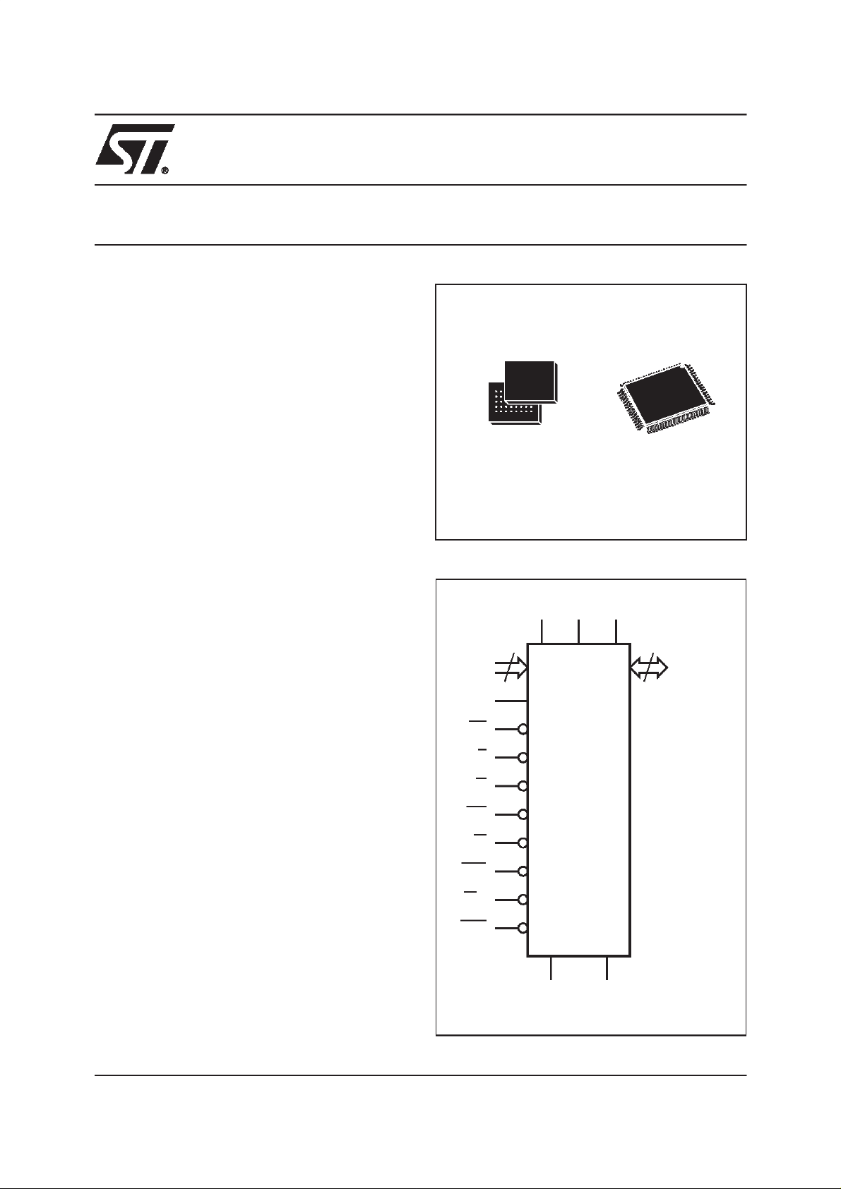
BGA
LBGA80 (ZA)
10 x 8 solder balls
Figure 1. Logic Diagram
V
V
DD
DDQVPP
18
A17-A0
CLK
RP
E
G
GD
W
LBA
WR
BAA
M58BF008
V
SS
M58BF008
PRELIMINARY DATA
PQFP80 (D)
32
DQ31-DQ0
V
SSQ
AI02656B
February 2000
This is preliminary information on a new product now in development or undergoing evaluation. Details are subject to change without notice.
1/36
Page 2
M58BF008
Figure 2. LBGA Connections (Top view through package)
87654321
A16 A9
A14A17B
DQ3DQ4D
G
A12 A10
V
DDQ
V
SSQ
V
DDQ
V
SSQ
A11A13A15A
V
DD
DU
DU DU
DU DU
V
DDQ
V
V
SS
PP
DU
V
V
V
V
DDQ
SSQ
SSQ
DDQ
DQ30
DQ26DQ6DQ8F
A3A4A8
A2A1A6A7
DQ31A5A0DQ0DQ2DQ1C
DQ28
DQ27DQ29DQ5DQ7E
DQ25
DQ24DQ23DQ9DQ10
2/36
H
J
K
RP
BAADQ12DQ11
LBA
V
SS
G
E
DD
W
WR
DQ19DQ201DQ22V
DQ17DQ21DQ18CLKDQ13DQ14
DQ16DUGDDQ15
AI02668
Page 3
Figure 3. PQFP Connections
GDWRWNCG
NC
M58BF008
SS
DD
E
V
LBA
BAA
V
NC
NC
CLK
RP
DDQ
V
DQ16
DQ17
DQ18
DQ19
V
DDQ
V
SSQ
DQ20
DQ21
DQ22
DQ23
DQ24
DQ25
DQ26
DQ27
V
DDQ
V
SSQ
DQ28
DQ29
DQ30
DQ31
NC
A0
A1
A2
1
12
73
M58BF008 53
32
DQ15
DQ14
DQ13
DQ12
V
SSQ
V
DDQ
DQ11
DQ10
DQ9
DQ8
DQ7
DQ6
DQ5
DQ4
V
SSQ
V
DDQ
DQ3
DQ2
DQ1
DQ0
NC
NC
A17
A16
A3
A4
A5
A6
A7
A8
V
SS
V
PP
V
DD
A9
A10
A11
A12
A13
A14
AI02661
A15
3/36
Page 4
M58BF008
Table 1. Signal Names
A0-A17 Address Inputs
DQ0-DQ31 Data Input/Output
CLK System Clock
RP Reset/Power-down
E Chip Enable
G Output Enable
GD Output Disable
W Write Enable
LBA Load Burst Address
WR Write/Read
BAA Burst Address Advance
V
DD
V
DDQ
V
PP
V
SS
V
SSQ
NC Not Connected Internally
DU Don’t Use as Internally Connected
Supply Voltage
Supply Voltage for Input/Output
Buffers
Program Supply Voltage
Ground
Input/Output Ground
A Command Interface decodes the Instructions
written to the memory to access or modify the
memory content, to toggle the enable/disable of
read access to the Overlay block, to toggle the
burst Wrap/No-wrap or to toggle the Synchronous
or Asynchronous Read mode. A Program/Erase
Controller (P/E.C.) executes the algorithms taking
care of the timings necessary for program and
erase operations. The P/E.C. also takes care of
verification to unburden the system microprocessor, while a Status Register tracks the status of
each operation.
The following Instructions are executed by the
memory in either Asynchronous or Synchronous
mode.
Access or modify memory content:
- Read Array
- Read or Clear Status Register
- Read Electronic Signature
- Erase Main memory block or Overlay block
- Program Main memory or Overlay memory
- Program Erase Suspend or Resume
Toggle:
– Asynchronous/Synchronous Read
– Overlay Block Read Enable/Disable
– Burst Wrap/No-wrap
The M58BF008 devices are offered in PQFP80
and LBGA80 1.0mm ball pitch packages.
When the VPPsupply is at VSSthis prevents programming and erasure of the memory blocks and,
in addition, it prevents reading of the Overlay
block. When the VPPsupply is at 5V it enables
both in-system program/erase and read access to
the Overlay block. For a limited time and number
of program/erase cycles the VPPsupply may be
raised to 12V to provide fast program and erase
times.
Table 2. Absolute Maximum Ratings
Symbol Parameter Value Unit
T
A Ambient Operating Temperature
T
BIAS
T
STG
V
IO
V
DD,VDDQ
V
PP
Note: 1. Stresses above those listed in the Table”Absolute Maximum Ratings” may cause permanent damage to thedevice.
Temperature Under Bias –40 to 125 °C
Storage Temperature –55 to 150 °C
Input Output Voltage
Supply Voltage –0.6 to 7 V
Program Voltage –0.6 to 13.5 V
(1)
–40 to 125 °C
–0.6 to V
DDQ
+0.6
V
4/36
Page 5
M58BF008
ORGANISATION
The M58BF008 has a data path width of 32 bit
(Double-Word) and isorganised as a Main memory array of 32 blocks of 256 Kbit plus an Overlay
block of 256 Kbit having the same address space
as the first Main memory block. The memory map
is shown in Table 3.
The memory is addressed by A0-A17 which are
static for Asynchronous or latched for Synchronous operation. Data Input/Output is static or
latched on DQ0-DQ31, these signals output data,
Table 3. Block Addresses
#
31 256 3E000-3FFFF
30 256 3C000-3DFFF
29 256 3A000-3BFFF
28 256 38000-39FFF
27 256 36000-37FFF
26 256 34000-35FFF
25 256 32000-33FFF
24 256 30000-31FFF
23 256 2E000-2FFFF
22 256 2C000-2DFFF
21 256 2A000-2BFFF
20 256 28000-29FFF
19 256 26000-27FFF
18 256 24000-25FFF
17 256 22000-23FFF
16 256 20000-21FFF
15 256 1E000-1FFFF
14 256 1C000-1DFFF
13 256 1A000-1BFFF
12 256 18000-19FFF
11 256 16000-17FFF
10 256 14000-15FFF
9 256 12000-13FFF
8 256 10000-11FFF
7 256 0E000-0FFFF
6 256 0C000-0DFFF
5 256 0A000-0BFFF
4 256 08000-09FFF
3 256 06000-07FFF
2 256 04000-05FFF
1 256 02000-03FFF
0 256 00000-01FFF
Overlay Block 256 00000-01FFF
Size
(Kbit)
Address Range
status orsignatures read from thememory, or they
input data to be programmed or Instruction commands to the Command Interface.
Asynchronous mode
Memorycontrol isprovidedby ChipEnable E, Output Enable G and Write Enable W for read and
write operations.
Synchronous mode
Memorycontrol isprovided byLoad BurstAddress
LBA which loads a read or write address. A Synchronous Single Read or a Synchronous Burst
Read is performed under control of Output Enable
G. Synchronous Write is controlled by Write/Read
Enable WR, Load Burst Address LBA and Write
Enable W. Internal advance of theburst address is
controlled by Burst Address Advance BAA.
SIGNAL DESCRIPTIONS
See Figure 1 and Table 1.
Address Inputs (A0-A17). The address signal
A17 is the MSB and A0 the LSB.
In theAsynchronous mode the addresses must be
stable before Chip Enable E and Write Enable W
go to VIL. They mustremain stable during the read
or write cycle.
In the Synchronous modes, the addresses are
latched by the rising edge of the System Clock
CLK when both Latch Burst Address LBA and
Chip Enable E are at VIL. The addresses are
latched fora read operation if Write/ReadWR is at
VIHor for a write operation when it is at VIL.
Data Input/Output (DQ0-DQ31). The data signal
DQ31 is the MSB and DQ0 the LSB. Commands
are input on DQ0-DQ7.
Data input is a Double-Wordto beprogrammed in
the memory or an Instruction command to the
Command Interface.Data is read from theMain or
Overlay memory blocks, the Status Register orthe
Electronic Signature.
In the Asynchronous mode data is read when the
addresses are stable and Chip EnableE and Output Enable G are at VIL. Commands or address/
data are written when Chip Enable E and Write W
are at VIL.
In the Synchronous mode, after addresses are
latched, data is read on a rising edge of the System Clock CLK when Chip Enable E is at VILand
if Output Enable was at VILon the previous rising
clock edge. Data is written on a rising edge of the
System Clock CLK when Chip EnableE and Write
Enable W are at VIL.
The outputs are high impedance when Chip Enable E or OutputEnable G are atVIH, or whenOutput Disable GD is at VIL. Outputs are also high
impedance when System Reset RP is at VIL.
5/36
Page 6

M58BF008
System Clock (CLK). All synchronous signals
are input and output relative to the System Clock.
Synchronous input signals must respect the setup and hold times relative to theSystem Clock rising edge.
Reset/Power-down (RP). The Reset/Power-
down RP input provides a hardware reset for the
memory. When Reset/Power-down RP is at V
IL
the memoryis reset and in thePower-down mode.
In this mode the outputs are high impedance and
the current consumption is minimised. When Reset/Power-down RP is at VIHthe memory is in the
normal operating mode. When leaving the Powerdown mode the memory entersthe Asynchronous
Read Array mode.
Reset/Power-down has a weak pull-up resistor to
V
and will assume a high level if not connect-
DDQ
ed.
Chip Enable (E). When the Chip Enable E input
is at VILit activates the memory control logic, input
buffers, decoders and sense amplifiers. When
Chip Enable E is at VIHthe memory is deselected
and the power consumption is reduced to the
standby level.
Output Enable (G). Output EnableG controls the
data output buffers. In the Asynchronous mode
data is output when Output Enable G is at VIL.In
the Synchronous mode, Output Enable G is sampled on the rising edge of the System Clock CLK.
If OutputEnable E is at VILthen valid output data
on DQ0-DQ31 can be read at the next risingedge
of the System Clock CLK.
Output Disable (GD). In the Asynchronous
mode thedata outputsDQ0-DQ31 arehigh impedance when Output Disable GD is at VIL, irrespective of the state of Output Enable G. In
Synchronous mode Output Disable GD is sampled, together with Output Enable G, on the rising
edge of the System Clock CLK. If Output Disable
is at VILthenthe data outputsDQ0-DQ31 arehigh
impedance at the next rising edge of the System
Clock CLK, irrespective of the state of Output Enable G.
Output Disable has a weak pull-up resistor to
V
and willassume a high level if not externally
DDQ
connected.
Write Enable (W). The Write Enable W input
controls the writing of commands or input data. In
the Asynchronous mode commands or data are
written when Chip Enable E and Write Enable W
are at VIL. In the Synchronous mode with Chip Enable E at VIL, input data is sampledif Write Enable
WisatVILon the rising edge of the System Clock
CLK.
Load Burst Address (LBA). In the Asynchronous mode LoadBurst Address LBA isDon’t Care
(but if it falls during an asynchronous read then a
new read cycle is started). In the Synchronous
mode Load BurstAddress LBAenables latching of
the burst starting address forSynchronous read or
write. The address is latchedon the rising edge of
the System Clock CLK if Load Burst Address LBA
is at VIL.
Write/Read (WR). Write/Read WR is used in
Synchronous mode to control write or readoperations. If Load Burst Address LBA is at VILand
Write/Read is at VILthen the rising edge of the
System Clock CLK latches a write address. If
Write/Read is at VIHthen a read address is
latched.
Write/Read has a weak pull-up resistor to V
DDQ
and will assume a high level if not externally connected.
Burst Address Advance (BAA). When Burst
Address Advance BAA is at VIL, the rising edge of
the System Clock CLK advances the burst address. When BurstAddress AdvanceBAA isat V
IH
the advance is suspended.
VDDSupply Voltage. The supply VDDprovides
the power to the internal circuits of the memory.
The VDDsupply voltage is 4.5 to 5.5V.
V
Input/Output Supply Voltage. The Input/
DDQ
Output supply V
provides thepower for the in-
DDQ
put/outputs of the memory, independent from the
supply VDD. The Input/Output supply V
DDQ
may
be connected to the VDDsupply or it can use a
separate supply of 3.0 to 3.6V.
VPPProgram/Erase Supply Voltage. The Program/Erase supply VPPis used for programming
and erase operations. The memory normally executes program and erase operations at the supply
V
voltage levels.
PP1
In a manufacturing environment, programming
may be speeded upby applying ahigher V
PPH
level to the VPPProgram/EraseSupply. Thisis not intended forextended use. The V
supply may be
PPH
applied for atotal of 80 hours maximumand during
program anderase for a maximum of 1000 cycles.
Stressing the device beyond these limits could
damage the device.
When VPPProgram/Erase supply is at VSSall
blocks are protected from programming or erase.
Leaving VPPfloating is equivalent to connecting it
to VSSdue to an internal pull-down circuit.
Ground (VSSand V
). The Ground VSSis t he
SSQ
reference for the internal supply voltage VDD.The
Ground V
supply V
is the reference for the Input/Output
SSQ
.
DDQ
6/36
Page 7
M58BF008
DEVICE OPERATIONS
See Table 4 for Asynchronous or Synchronous
Bus Operations.
In theAsynchronous modethe memoryis selected
with Chip Enable E Low. The data outputs are enabled by Output Enable G Low or disabled by Output Disable GD Low. Datais input byWrite Enable
W Low.
In the Synchronous mode the memory latches addresses and data (input or output) on the rising
edge of the System Clock CLK. Burst address
latching is enabled by Load Burst Address LBA
Low with Write/Read WR Low for a write cycle or
High for a read cycle.
Data outputs are enabled for reading on the rising
edge of the System Clock CLK when Output Enable G is low. Data is input on the rising edge of
the System Clock CLK when Write Enable W is
Low.
power-down mode when Reset/Power-Down RP
is Low.
Read. Read operations are used to output the
contents of the memory, the Electronic Signature
or the Status Register. The data read depends on
the previous Instruction given to the memory.
Read operations can be Asynchronous or Synchronous, witha single or burst read.On power-up
the device is in Asynchronous read mode, the Instruction Asynchronous/Synchronous Read Toggle ART can be used to enter the Synchronous
read mode.
– Asynchronous Read. To read a data Double-
Wordin Asynchronousmode the address inputs
must be stable and Chip Enable E must be Low
during theread cycle. Output Enable Gmust be
Low and Output Disable GD High. The Load
Burst Address LBA is Don’t Care, but its falling
edge will start a new read cycle.
The memory is deselected and in standby mode
when Chip Enable E is High, and it is reset or in
Table 4. Bus Operations
Operation RP CLK E LBA WR W GD G DQ0-DQ31
Asynchronous Read
Asynchronous Write
Synchronous Read
Synchronous Write Address for
Read
Synchronous Write Address for
Command
Synchronous Data Write
Output Disabled by G
Output Disabled by GD
Standby
Reset / Power-down
Note: 1. See Device Operations, Instructions and Commands, sections for more details.
2. X=V
or V
IL
IH.
(1,2)
V
IH
V
IH
V
IH
V
IH
V
IH
V
IH
V
IH
V
IH
V
IH
V
IL
V
X
V
X
V
V
V
V
V
X
V
X
V
X
XX
IL
XX
IL
V
IL
V
IL
V
IL
V
IL
IL
IL
IH
V
IH
IL
IL
IH
IH
V
IH
V
IL
V
IH
XXX
XXX
XXXXX Hi-Z
XXXXXXX Hi-Z
V
V
V
IH
IL
X
X
IH
V
IH
V
IH
V
IH
XVIHV
V
V
IL
IH
V
IH
V
IL
V
V
V
V
V
V
IL
IH
IL
IH
IH
IH
IH
Data Output
Data Input
Data Output
Data Input
Hi-Z
X Hi-Z
X
X
Table 5. Read Electronic Signature
Code RP E G W A0 A1 A2-A17 DQ0-DQ31
Manufacturer
Device
Version
Note: ”x” = version level. The first version is ”0” and it can have a value up to ”7”.
V
IH
V
IH
V
IH
V
IL
V
IL
V
IL
V
IL
V
IL
V
IL
V
IH
V
IH
V
IH
V
IL
V
IH
V
IL
V
IL
V
IL
V
IH
Don’t Care 00000020h
Don’t Care 000000F0h
Don’t Care 0000000xh
7/36
Page 8

M58BF008
– Synchronous Single Read. To read a single
data Double-Word in Synchronous mode Chip
Enable E must be Low. Load Burst Address
LBA must be Low for one System ClockCLK rising edgewith Write/Read WRHigh. This latches
the read address, after which the address bus
inputs are Don’t Care. The Output Enable G is
Low for a single System Clock CLK cycle. The
Double-Word of valid data is output on the next
System Clock CLK rising edge.
– Synchronous Burst Read. To read a burst of
four Double-Words in Synchronous mode Chip
Enable /E must be Low. Load Burst Address
LBA must be Low for one System ClockCLK rising edgewith Write/Read WRHigh. This latches
the first address of the burst sequence, after
which the address bus inputs are Don’t Care.
The Output Enable G is driven Low before the
burst output sequence. Four Double-Words of
data are output on the subsequent System
Clock CLK rising edges if Burst Address Advance BAA is maintainedLow. The address advance for synchronous burst read is suspended
if Burst Address Advance BAA goes High and
the output data remains constant. The data bus
will go high impedanceon the rising edge ofthe
System Clock CLK after Output Enable G goes
High.
The burst timing depends on the device configuration for theCritical Word X and BurstWord Y
latency times and the choiceof wrap orno-wrap
for burst addresses. The operation burst wrap is
shown in Table 13. The wrap sequence uses
only the address bits A0 and A1 and does not
repeat after the last Double-Wordhas been output.
Read Overlay Block. The Overlay block can be
read, as for a Main block, after it has been enabled. To enable the Overlay block the Overlay
Block Enable bit OBEB and the OverlayBlock Status bit OBS in the Status Register must be set to
’1’- see Table 9.
The Overlay Block Enable bit OBEB can be set to
’1’in three ways - see Table 10:
– By Toggling the Reset/Power-Down signal RP
with the VPPProgram/Erase supply in the range
V
PP1
or V
PPH.VPP
out of range will reset the
OBEB bit to ’0’.
– By a leaving power-on reset with VPPProgram/
Erase supplyin the rangeV
PP1
orV
PPH.VPP
out
of range will reset the OBEB bit to ’0’.
– By giving the Overlay Block Enable/Disable for
Read Instruction OBT.
The Overlay Block Status bit OBS monitors the
VPPProgram/Erase supply and will be set to ’1’
when in the range V
PP1
or V
. The Overlay
PPH
block is enabled with OBEB at ’1’ but will not be
read unless OBS status bit is also at ’1’. If it is not
then a read operation will read the contents of the
Main block at the same address.
When the Overlay block is enabled for reading,
only this one block of 256 Kbit is accesible and
none of the other Main blocks may be accessed,
the address signals A13-A17 are Don’tCare.
Read Electronic Signature. The memory contains three Electronic Signature codes identifying
the manufacturer, device and version, which can
be read after giving the Instruction RSIG. The
manufacturer code 00000020h is read when the
address inputs A0 and A1 are at VIL. The device
code 000000F0his read when A0 isat VIHand A1
is at VIL. The version code 0000000xh is read
when A0 is at VILand A1 is at VIH. The codes are
read on DQ0-DQ31,all other address signalinputs
are Don’t Care. See Table 5.
Write. Write operations are used to give commands tothe memory that latch input data and addresses to program or block addresses to erase.
– Asynchronous Write. To write data in the
Asynchronous mode the address inputs must
be stable and Chip Enable E must be Low during thewrite cycle. WriteW mustbe Low andinput data valid on the rising edge is Write W.
– Synchronous Write. To write input data in
Synchronous mode Chip Enable E must be
Low. Load Burst Address LBA must be Low for
one System Clock CLK rising edge with Write/
Read WR Low. This latches the write address,
after which the address bus inputs are Don’t
Care. WhenWrite EnableW isLow input datais
latched on the next System Clock CLK rising
edge.
Output Disable. The data outputs are high impedance when the Output Enable G is High or
when the Output Disable GD is Low, independent
of the level on Output Enable G.
Standby. The memory is in standby when the P/
E.C. is not running, the memory is in read mode
and Chip Enable E is High. The power consumption is reducedto the standby level and the outputs
are high impedance, independent of the Output
Enable G or Write Enable W inputs.
If Chip Enable goes High during a program or
erase operation the device enters the standby
mode when the internal algorithm has finished.
Reset/Power-down. During power-down all internal circuits are switched off, the memory is deselected and the outputs arehigh impedance. The
memoryis inPower-down mode whenReset/Power-down RP isLow. The power consumption is reduced to thepower-down level,independent of the
Chip Enable E, Load Burst Address LBA, Output
Enable G or Write Enable W inputs.
If Reset/Power-down RP is pulled Low during a
program or erase operation thisis aborted and the
memory content is no longer valid.
8/36
Page 9
M58BF008
INSTRUCTIONS AND COMMANDS
The Instructions are listed in Tables 6 and 7. They
may be broadly divided into two types, those that
access or modify the memory content and those
that toggle a mode or function.
The Instructionsthat access ormodify the memory
content include:
– Read Memory Array (RD)
– Read Status Register (RSR) and Clear Status
Register (CLRS)
– Read Electronic Signature (RSIG)
– Erase (EE) and OverlayBlock Erase (OBEE)
– Program (PG) and Overlay Block Program (OB-
PG)
– Program or Erase Suspend (PES) and Program
or Erase Resume (PER)
The Instructions that toggle a mode or function in-
clude:
– Asynchronous/Synchronous Read mode Tog-
gle (ART)
– Wrap/No-wrap Burst mode Toggle (WBT)
– Overlay Block Enable/Disable function Toggle
(OBT)
Instructions are written, in one or more write cy-
cles, to the memory Command Interface (C.I.) for
decoding. The Command Interface is reset to
Read Memory Array at power-up, when exiting
from power-down. Any invalid sequence of commands will also reset the Command Interface to
Read Memory Array.
A Program/Erase Controller (P/E.C.) handles all
the timing and verifies the correct execution of the
Program or Erase instructions. The P/E.C. has a
Status Register which monitors the operations and
which may be read at any time during program or
erase. The Status Register bits indicate the operation and exit status of the internal algorithms.
The VPPProgram and Erase Supply Voltage must
be withinthe range V
PP1
orV
for programming
PPH
or erasure. If VPPout of range, the program or
erase algorithms do not start and Status Register
bit VPPStatus V
will be set to ’1’.
PPS
Table 6. Commands
Code Command
02h Overlay Block Erase Set-up
04h Overlay Block Program Set-up
06h
0Dh Overlay Block Erase Confirm
20h Erase Set-up
30h Wrap/No-wrap Burst Toggle
40h Program Set-up
50h Clear Status Register
60h
70h Read Status Register
90h Read Electronic Signature
B0h Program/Erase Suspend
D0h
FFh Read Memory Array
Overlay Block Read Enable/
Disable
Asynchronous/Synchronous
Read Toggle
Program/Erase Resume or
Erase Confirm
9/36
Page 10
M58BF008
Table 7. Instructions
Mne-
monic
RD
RSR
CLRS
RSIG
EE Erase 2 Write 00000h 20h Write Block Address D0h
Instruction Cycles
Read Memory
Array
Read Status
Register
Clear Status
Register
Read Electronic
Signature
Operation Address Data Operation Address. Data
1+ Write 00000h FFh
1+ Write 00000h 70h Read X
1 Write 00000h 50h
1+++ Write 00000h 90h Read
1st Cycle 2nd Cycle
Read
Read Address Data Output
Signature
Address
Status
Register
Electronic
Signature
OBEE
PG Program 2 Write 00000h 40h Write
OBPG
PES
PER
ART
WBT
OBT
Read Memory Array (RD). The Read Memory
Array instruction consists of one write cycle giving
the command FFh atthe address 00000h. Subsequent read operations will read the addressed location and output the memory data. The data can
be read from the Main memory Array or the Overlay memory block if it is enabled.
Read Status Register (RSR). The Read Status
Register instructionconsists ofone write cycle giving thecommand 70h attheaddress 00000h.Subsequent read operations will output the Status
Register contents. See Table 8 for an explanation
of the Status Register bits. TheStatus Register indicates when a program or Erase operation is
complete and its success or failure. The Status
Register also indicates if the Overlay block is accessible for reading. The Read Status Register instruction may be given at anytime, including while
Overlay Block
Erase
Overlay Block
Program
Program/Erase
Suspend
Program/Erase
Resume
Asynch/Synch
Read Toggle
Wrap//No-wrap
Burst Toggle
Overlay Block
Read En/Dis
Toggle
2 Write 00000h 02h Write
2 Write 00000h 04h Write
1 Write 00000h B0h
1 Write 00000h D0h
1 Write 00000h 60h
1 Write 00000h 30h
1+ Write 00000h 06h Read Read Address Data Output
Clear Status Register (CLRS). The Clear Status
Register instructionconsists of onewrite cycle giving the command 50h at the address 00000h.The
Clear Status Register command clears the bits 3,
4 and 5 of the Status Registerif theyhavebeen set
to ’1’ by the P/E.C. operation. The Clear Status
Register command should be given after an error
has been detected and before any new operation
is attempted. A Read Memory Array command
should also be given beforedata can beread from
the memory array.
Read Electronic Signature (RSIG). The Read
Electronic Signature instruction consists of a first
write cycle giving the command90h atthe address
00000h. This is followed by three read operations
at addresses xxxx0h, xxxx1h and xxxx2h which
output the manufacturer, device and version
codes respectively.
a program or erase operation in progress.
Overlay Block
Address
Program
Address
Overlay Block
Program
Address
0Dh
Data Input
Data Input
10/36
Page 11
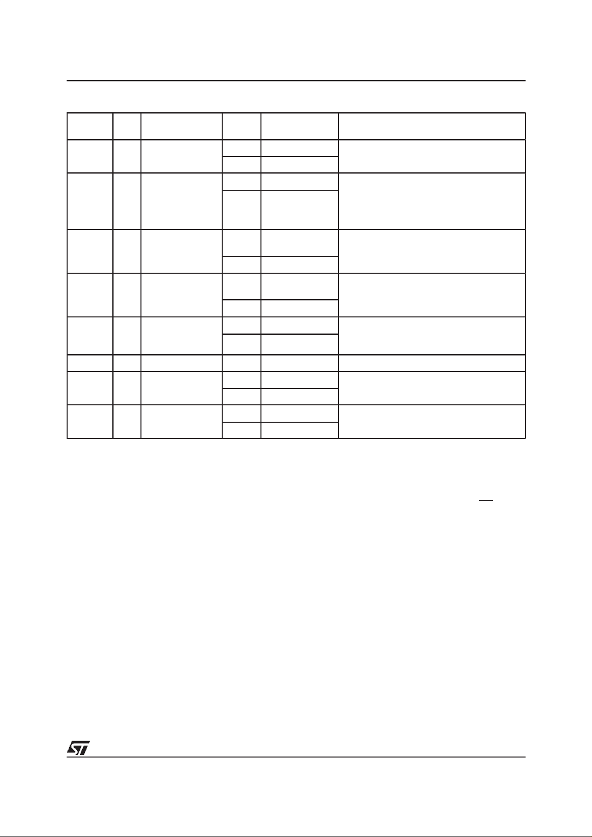
Table 8. Status Register Bits
Mne-
monic
P/ECS 7 P/E.C. Status
PESS 6
ES 5 Erase Status
Bit Name
Program/Erase
Suspend Status
M58BF008
Logic
Level
’1’ Ready
’0’ Busy
‘1’ Suspend On Program/Erase Suspend instruction both
‘0’
’1’ Erase Error or
’0’ Erase Success
Definition Note
Indicates the P/E.C. status, check during
Program or Erase
P/ECS and PESS bits are set to ‘1’.
In Progress or
Completed
Erase Suspend
Either ES bit or PS bit is set to ‘1’.
PESS and either ES or PS bits remain at ‘1’
until Erase Resume instruction is given.
ES bit is set to ‘1’ if either PESS instruction is
given or Erase operation fails. If ES bit is ‘1’,
check PESS bit.
’1’ Program Error or
PS 4 Program Status
V
VPPS 3
Reserved 2
OBEB 1
OBS 0
Status
PP
Overlay Block
Enable Bit
Overlay Block
Status
Program Suspend
’0’ Program Success
V
’1’
’0’
’1’ Enabled
’0’ Disabled
’1’ Activated
’0’ Not Activated
PP
V
PP
Erase (EE). The Erase instruction consists oftwo
write cycles, the first is the eraseset-up command
20h at theaddress 00000h. Thisis followed by the
Erase Confirm command D0h written to an address within the block to be erased. If the second
is not the Erase Confirm command the Status
Register bits 4 and 5 are set to ’1’and the instruction aborts. While erasing is in progress only the
Read Status Registerand Erase Suspend instructions are valid.
Blocks are erased one at a time. An erase operation sets all bits in a block to ’1’. The erase algorithm automatically programs all bits to ’0’ before
erasing the block to all ’1’s.
Read operations output the Status Register after
the erase operation has started. The Status Register bit 7 is ’0’ whilethe erase is in progress andis
set to’1’when it is completed.After completionthe
Status Register bit 5 is set to ’1’ if there has been
an erase failure.
Erasure should not be attempted when the V
PP
Program/Erase Supply Voltage is out of the range
V
PP1
or V
as the results will be uncertain. The
PPH
PS bit is set to ‘1’ if either PESS instruction is
given or Program operation fails.If PSbit is ‘1’,
check PESS bit.
Invalid VPPS bit is set to ‘1’ if initially VPPis not V
OK
nor V
are executed.
OBEB bit is set to ‘1’ when OverlayBlock is
Enabled.
OBS bit is set to ‘1’ when OBEB is ‘1’ and V
is in the range V
, when Program or Erase Instruction
PP1
PP1
or V
PPH
.
Status Register bit 3 is set to’1’ if VPPis not within
the allowedranges whenerasing is attempted or if
it falls out of the ranges during erase execution.
The erase operation aborts if VPPdrops out of the
allowed range or if Reset/Power-down RP falls to
VIL. As data integrity cannot be guaranteed when
the erase operation is aborted, the erase must be
repeated.
A Clear Status Register instruction must be given
to clear the Status Register bits.
Overlay Block Erase (OBEE). The Overlay
Block Erase instruction consists of two write cycles, the first is the Overlay block erase set-up
command 02h at the address 00000h. This is followed by the Overlay Block Erase Confirm command 0Dh written to an address withinthe Overlay
block. If the secondis not the Overlay Block Erase
Confirm command the Status Register bit 5 is set
to ’1’ and theinstruction aborts. While erasing is in
progress only theRead Status Register instruction
is valid.
The operation is executed as described for the
Erase (EE) instruction of the Main memory array.
A Clear Status Register instruction must be given
to clear the Status Register bits.
PPH
PP
11/36
Page 12

M58BF008
Program (PG). The Program instruction consists
of two write cycles, the first is the program set-up
command 40h at the address 00000h. This is followed by asecond write cycle tolatch the address
and data to be programmed. This second command starts the P/E.C. A program operation can
be aborted by writing FFFFFFFFh to any address
after the program set-up command has been given. While programming is in progress only the
Read Status Register and Program Suspend instructions are valid.
Read operations output the Status Register after
the program operation has started. The Status
Register bit 7 is ’0’ while programming is in
progress and is set to ’1’ when it is completed. After completion the Status Register bit 4 is set to ’1’
if there has been a programming failure.
Programming should not be attempted when the
VPPProgram/Erase Supply Voltage is out of the
range V
PP1
or V
as the results will be uncer-
PPH
tain. The Status Register bit 3 is set to ’1’if VPPis
not within the allowed ranges when programming
is attempted or if it falls out of the ranges during
program execution.
The program operation aborts if VPPdrops out of
the allowed ranges or if Reset/Power-Down RP
falls to VIL. As data integrity cannot beguaranteed
when the program operation is aborted, the memory block must be erased and programming repeated.
A Clear Status Register instruction must be given
to clear the Status Register bits.
Overlay Block Program (OBPG). The Overlay
Block Program instruction consists of twowrite cycles, the first is the program set-up command 04h
at the address 00000h. This is followed by a second write cycle to latch theaddress and data to be
programmed. This second command starts the P/
E.C.
The operation is executed as described for the
Program (PG) instruction of the Main memory array.
While programming of the Overlay block in
progress onlythe ReadStatus Registerinstruction
is valid.
Program/Erase Suspend (PES). As memory
erasure takes of the order of seconds to complete
and programming a few microseconds, a Program/Erase Suspend instruction is implemented.
Program/Erase Suspend interrupts the operations
to allow reading or programming in a block other
than one in whichprogram or erase is suspended.
A Program/Erase Suspend instruction is accepted
only during a Program or Erase instruction. When
the Program/Erase Suspend command is written
to the Command Interface, the P/E.C. freezes the
program or erase operation. The suspended program orerase operation maybe restartedby using
the Program/Erase Resume instruction. Program/
Erase Suspend is not allowed during the Overlay
block program/erase operation and the command
is ignored.
The Program/Erase Suspend instruction consists
of one write cycle giving the command B0h at the
address 00000h.
If a program operation is in progress when the instruction is given, the Status Register bits 4 and 6
are set to ’1’ after it has been suspended. If an
erase operation is in progress when theinstruction
is given, the Status Register bits 5 and 6 are set to
’1’after it has been suspended.
The valid instructions that may be given to the
memory while programing is suspended are
– Read Memory Array (RD)
– Read Status Register (RSR)
– Read Electronic Signature (RSIG)
– Program/Erase Resume (PER)
In addition, while erasure is suspended, the Pro-
gram (PG) instruction may be given.
In Program/Erase Suspendmode the memory can
be placed in a pseudo-standby mode by taking
Chip Enable /E to VIH to reduce power consumption.
Program/Erase Resume (PER). If a Program/
Erase Suspend instruction has previously been
executed, then the operation may be resumed by
giving the command D0h at the address 00000h.
The Status Register bits 4, 5 and 6 are cleared
when programor erase resumes.A Read Memory
Array instructionwill output theStatus Register after program or erase is resumed.
Suggested flow charts for software that uses programming, erasure and program/erase suspend/
resume operations are shown in Figures 11, 12,
13 and 14.
Asynchronous/Synchronous Rea d Toggle (ART).
Asynchronous Read Memory Array is thememory
default atpower-up or whenreturning from PowerDown. To read data in Synchronous mode, either
single or burst, the Asynchronous/Synchronous
Read Toggle instruction must be used.
The Asynchronous/Synchronous Read Toggle instruction consists of one write cycle giving the
command 60h at the address 00000h. Two consecutive instructions are not recognised and another Instruction, for example the Read Memory
Array, must be given before another Asynchronous/Synchronous Read Toggle will be recognised.
12/36
Page 13

M58BF008
Wrap/No-wrap Burst Toggle (WBT). The de-
fault for burst read is set by the device configuration. The Wrap/No-wrap Burst Togglecan be used
to toggle the burst wrap operation.
The Wrap/No-wrap Burst Toggle instruction consists of onewrite cycle giving the command 30h at
the address 00000h. Two consecutiveinstructions
are not recognised and another Instruction, for example the Read Memory Array, must be given be-
Overlay Block Read Enable/Disable Toggle
(OBT). Read operations in the Overlay block can
be enabled or disabled using the Overlay Block
Read Enable/Disable Toggle instruction. This toggle instruction consists of one write cycle giving
the command 06h at the address 00000h. Two
consecutive instructions are not recognised.
The Status Register bit 1 is set to ’1’ when the
Overlay block is enabled.
fore another Wrap/No-wrap Burst Toggle will be
recognised.
Table 9. Read Access to Overlay Block or Main Block
OBEB Status Bit
1
1
0 X 0 Main Block
1 Unknown Not guaranteed Unknown
In the range V
V
PP
or V
PP1
Out of the range
V
or V
PP1
PPH
PPH
Table 10. Overlay Block Enable/Disable Bit (OBEB)
Method
In the range
V
ToggleRP
Power-on-reset
Overlay Block Read Enable/Disable instruction OBT
Note: 1. Toggle H-L-H for t
(1)
PLPH
minimum.
PP1
Out of the range
V
PP1
In the range
V
PP1
Out of the range
V
PP1
OBS Status Bit Read Access
1 Overlay Block
0 Main Block
OBEB Status Bit
V
PP
or V
PPH
or V
PPH
or V
PPH
or V
PPH
–01
–10
Prior state of
OBEB
X1
X0
X1
X0
Next state of
OBEB
13/36
Page 14

M58BF008
CONFIGURATION
The M58BF008 is configured during testing which
sets the default for the write and burst interface.
The settings are:
Write Interface. The write interface can be set
permanently to either Asynchronous or Synchronous. Note that the read interface is not affected
by thisconfiguration and defaults to Asynchronous
read at power-up, it can be toggled to Synchronous read and back using the Asynchronous/Synchronous Read Toggle Instruction.
Wrap/No-Wrap. The burst function can be set to
default to wrap or no-wrap. The behaviour is
shown in Table 13. Wrap/No-wrap can be toggled
using the Wrap/No-wrap Burst Toggle Instruction.
Critical Word and Burst Word Latency Times.
The Critical Word and Burst Word latency times
can be set permanently to
– Critical Word Latency Time X = 3 or 4
– Burst Word Latency Time Y = 1 or 2
A burst sequence is described as X-Y-Y-Y.
Table 11. Configuration
Name Option 1 Option 2
Write Interface Synchronous Asynchronous
Wrap/No-wrap Burst Wrap No-wrap
Critical Word Latency Time (X)
Burst Word Latency Time(Y)
43
12
Table 12. Wrap/No-wrap Burst Sequence
First Burst Address A1-A0 Data Wrap Data No-wrap
00 Double-Word 0 ⇒ 1 ⇒ 2 ⇒ 3 Double-Word 0 ⇒ 1 ⇒ 2 ⇒ 3
01 Double-Word 1 ⇒ 2 ⇒ 3 ⇒ 0 Double-Word 1 ⇒ 2 ⇒ 3
10 Double-Word 2 ⇒ 3 ⇒ 0 ⇒ 1 Double-Word 2 ⇒ 3
11 Double-Word 3 ⇒ 0 ⇒ 1 ⇒ 2 Double-Word 3
POWER SUPPLY
The M58BF008 places itself in one of three different modes depending on the status of the control
signals which define decreasing levels of current
consumption. This minimises the memory power
consumption, allowing an overall decrease in the
system power consumption without affecting performance. A different recovery time is, however,
linked to the different modes - see the AC timing
tables.
Active Power mode. When Chip Enable E is at
VILand Reset/Power-DownRP is atVIHthe memory is in Active Power mode. The DC characteristics tables show the current consumption figures.
Standby mode. Refer to the Device Operating
section
Power-Down mode. Refer to the Device Operating section.
14/36
Power Up. The VDDSupply Voltage, V
DDQ
Input/
Output Supply Voltage and the VPPProgram/
Erase Supply Voltage can beapplied in anyorder.
The memory Command Interface is reset on power-up to Read Memory Array, but a negative transition on Chip Enable E or a change of the
addresses is required to ensure valid data is output.
Care must be taken toavoid writes to the memory
when the VDDSupply Voltage is above V
LKO
and
VPPProgram/Erase Supply Voltage powers-up
first. Writes can be inhibited by driving either Write
Enable W or Write/Read WR to VIH.
The memory is disabled until Reset/Power-Down
RP is up to VIH.
SUPPLY RAILS
Normal precautions must be taken for supply rail
decoupling. Each device in a system should have
the VDD,V
and VPPrails decoupled with a
DDQ
0.1µF capacitor close to the package pins. PCB
track widths should be sufficient to carry the required program and erase currents on the V
PP
supply.
Page 15

M58BF008
Table 13. AC Measurement Conditions
Input Rise and Fall Times ≤ 10ns
Input Pulse Voltages
Input and Output Timing Ref. Voltages V
0toV
DDQ
DDQ
/2
Figure 5. AC Testing Load Circuit
V
/2
DDQ
1N914
3.3kΩ
Figure 4. AC Testing Input Output Waveform
DEVICE
UNDER
V
DDQ
V
/2
DDQ
0V
AI00610
Table 14. Capacitance
(1)
(TA=25°C, f = 1MHz)
Symbol Parameter Test Condition Min Max Unit
C
IN
C
OUT
Note: 1. Sampled only, not 100% tested.
Input Capacitance
Output Capacitance V
V
OUT
IN
TEST
CL= 80pF
CLincludes JIG capacitance
=0V
6pF
=0V 12 pF
OUT
AI02657
15/36
Page 16

M58BF008
Table 15. DC Characteristics
(TA= –40 to 125°C; VDD=5V±10% and V
Symbol Parameter Test Condition Min Max Unit
I
I
I
LT1
I
LIVPP
I
CC
I
CCB
I
CC1
I
CC2
I
CC3
I
CC4
I
I
PP1
I
PP2
I
PP3
Input Leakage Current
LI
Output Leakage Current
LO
Input Leakage Current pull-up
Input Leakage Current pull-down
Supply Current (Async. Read) E = VIL,G=VIL, f = 5MHz 25 mA
Supply Current (Burst Read)
Supply Current (Standby) E = VIH,RP=V
Supply Current (Power-down)
Supply Current (Program)
Program in Progress
Supply Current (Erase)
Erase in Progress
Program Current (Read or Standby)
PP
Program Current (Read or Standby)
Program Current (Power-down)
Program Current (Program)
Program in Progress
=3.3V ± 0.3V)
DDQ
E=V
0V≤ V
0V
0V≤ V
IL
≤ V
IN
DDQ
≤ V
OUT≤VDDQ
≤ V
IN
DDQ
0≤ V
≤ 12.6
PP
,G=VIL, f = 40MHz
IH
RP = V
IL
V
PP=VPP1
V
PP=VPPH
V
PP=VPP1
V
PP=VPPH
V
≥ V
PP
PP1
V
≤ V
PP
PP1
RP = V
IL
VPP=V
V
PP1
PP=VPPH
±1 µA
±10 µA
–20 –600 µA
200 µA
25 mA
10 µA
10 µA
25 mA
25 mA
25 mA
25 mA
200 µA
±15 µA
5 µA
15 mA
25 mA
I
V
V
V
V
V
V
PP4
V
IL
V
IH
OL
OH
PP1
PPH
LKO
PPLK
V
Program Current (Erase)
Erase in Progress
PP=VPP1
V
PP=VPPH
Input Low Voltage –0.3
Input High Voltage
Output Low Voltage
Output High Voltage
Program Voltage
(Program or Erase operations)
Program Voltage
(Program or Erase operations)
I
= 100µA,
OL
V
DD=VDD
V
DDQ=VDDQ
I
= –100µA,
OL
V
DD=VDD
V
DDQ=VDDQ
min,
min
min,
min
0.9V
V
DDQ
4.5 5.5 V
11.4 12.6 V
VDDSupply Voltage Lock-out
DDQ
–0.2
15 mA
25 mA
0.1V
DDQ
V
DDQ
+0.3
0.2 V
1.5 V
Program Voltage Lock-out 1.5 V
V
V
V
16/36
Page 17

M58BF008
Table 16. Asynchronous Read AC Characteristics
(TA= –40 to 125°C; VDD=5V±10% and V
DDQ
(1)
=3.3V ± 0.3V)
Symbol Alt Parameter Min Max Unit
t
AVAV
t
AVQV
(2)
t
AXQX
(2)
t
EHQX
(2, 3)
t
ELQV
(2)
t
ELQX
(2)
t
EXQZ
(2)
t
GHQX
(2)
t
GHQZ
(2)
t
GLQV
t
GLQX
Note: 1. See AC Testing Measurements Conditions for timing measurements.
2. Sampled only, not 100% tested.
3. G may be delayed up to t
t
t
ACC
t
t
t
t
t
t
t
t
t
OLZ
Address Valid to Next Address Valid 100 ns
RC
Address Valid to Output Valid 100 ns
Address Transition to Output Transition 0 ns
OH
Chip Enable High to Output Transition 0 ns
OH
Chip Enable Low to Output Valid 100 ns
CE
Chip Enable Low to Output Transition 0 ns
LZ
Chip Enable High to Output Hi-Z 25 ns
HZ
Output Enable High to Output Transition 0 ns
OH
Output Enable High to Output Hi-Z 25 ns
DF
Output Enable Low to Output Valid 30 ns
OE
Output Enable Low to Output Transition 0 ns
ELQV-tGLQV
after falling edge of E without increasing t
ELQV
.
Figure 6. Asynchronous Read AC Waveforms
A12-A29
tAVQV
E, LBA
tELQV
tELQX
G
tGLQX
tGLQV tGHQZ
DQ0-DQ31
tPHQV
RP
tAVAV
VALID
tEHQX
tEHQZ
tGHQX
VALID
AI03571
17/36
Page 18

M58BF008
Table 17. Synchronous Read AC Characteristics
(TA= –40 to 125°C; VDD=5V±10% and V
DDQ
(1)
=3.3V ± 0.3V)
Symbol Parameter Min Max Unit
DC
CLK
(2)
t
AVCH
t
BALCH
(2)
t
BLCH
(2)
t
CHAX
(2)
t
CHBH
t
CHCL
t
CHGDH
(2)
t
CHGH
(2)
t
CHQV
(2)
t
CHQX1
(2)
t
CHQX2
(2)
t
CHQZ
t
CLCH
t
CLCL
t
ELCH
(2)
t
GDLCH
(2)
t
GLCH
t
PHBL
t
WRHCH
Note: 1. See AC Testing Measurement Conditions for timing measurements.
2. Sampled only, not 100% tested.
System Clock Duty Cycle 45 55 %
Address Valid toSystem Clock High 10 ns
Burst Address Advance Low to System Clock High 10 ns
Load Burst Address Low to System Clock High 10 ns
System Clock High to Address Transition 5 ns
System Clock High to Load Burst Address High 5 ns
System Clock FallTime 3 ns
(2)
System Clock High to Output Disable High 5 ns
System Clock High to Output Enable High 5 ns
System Clock High to Data Valid 20 ns
System Clock High to Data Transition 0 ns
System Clock High to Data Transition 5 ns
System Clock High to Data Hi-Z 20 ns
System Clock Rise Time 3 ns
System Clock Period 25 ns
Chip Enable Low to System Clock High 20 ns
Output Disable Low to System Clock High 10 ns
Output Enable Low to System Clock High 10 ns
Reset/Power-down High to Load Burst Address Low 20 ns
Write/Read High to System Clock High 10 ns
18/36
Page 19

Figure 7. Synchronous Single Read AC Waveforms
CLK
tCHAXtAVCH
A0-A17
LBA
VALID
M58BF008
G
E
DQ0-DQ31
RP
WR
tBLCH
tELCH tCHQZtCHQV
tPHBL
tWRHCH
tCHBH
tGLCH tCHGH
tCHQX1
tCHQX2
VALID
AI02658
19/36
Page 20

M58BF008
Figure 8. Synchronous Burst Read AC Waveforms
CLK
tCHAXtAVCH
A0-A17
LBA
VALID
G
E
DQ0-DQ31
RP
WR
BAA
tBLCH
tELCH tCHQVtCHQV
tPHBL
tWRHCH
tCHBH
tGLCH
tCHQX1
tBALCH
VALID
tCHQX2
VALID
tCHQX2
AI03583
20/36
Page 21

M58BF008
Table 18. Asynchronous Write AC Characteristics
(TA= –40 to 125°C; VDD=5V±10% and V
DDQ
(1)
=3.3V ± 0.3V)
Symbol Alt Parameter Min Max Unit
t
AVAV
t
AVWH
t
DVWH
t
ELWL
t
PHWL
t
QVVPL
t
VPHWH
t
WHAX
t
WHDX
t
WHEH
t
WHQV1
t
WHQV2
t
WHWL
t
WLWH
Note: 1. See AC Testing Measurement conditions for timing measurements.
2. Sampled only, not 100% tested.
3. Time ismeasured to Status Register Read giving bit b7 = ’1’.
(2)
(2)
(3)
(3)
t
WC
t
t
t
t
t
VPS
t
t
t
t
WPH
t
WP
Write Cycle Time 70 ns
Address Valid to Write Enable High 70 ns
AS
Data Valid to Write Enable High 70 ns
DS
Chip Enable Low to Write Enable Low 0 ns
CS
Reset/Power-down High to Write Enable Low 70 ns
PS
Output Valid to VPPout of the range V
VPPHigh to Write Enable High
Write Enable High to Address Transition 0 ns
AH
Write Enable High to Data Transition 0 ns
DH
Write Enable High to Chip Enable High 0 ns
CH
PP1
or V
PPH
0ns
200 ns
Write Enable High to Output Valid, Program 10 µs
Write Enable High to Output Valid, Erase 2.1 sec
Write Enable High to Write Enable Low 30 ns
Write Enable Low to Write Enable High 70 ns
21/36
Page 22

M58BF008
Figure 9. Asynchronous Write AC Waveforms
A0-A17
00000h
tAVAV
VALID
G
E
W
DQ0-DQ31
V
PP
RP
WR
tELWL
tWLWH
tDVWH tWHDX
COMMAND
tPHWL
tWHAX
tWHEH
tWHWL
tVPHWH
COMMAND
or DATA
tAVWH
tWHQV1,2
STATUS
REGISTER
tQVVPL
22/36
WRITE WRITE READ
AI02660
Page 23

M58BF008
Table 19. Synchronous Write AC Characteristics
(TA= –40 to 125°C; VDD=5V±10% and V
DDQ
(1)
=3.3V ± 0.3V)
Symbol Parameter Min Max Unit
DC
CLK
(2)
t
AVCH
(2)
t
BLCH
(2)
t
CHAX
(2)
t
CHBH
t
CHCL
(3)
t
CHQV1
(3)
t
CHQV2
(2)
t
CHQX
(2)
t
CHWH
t
CHWRH
t
CLCH
t
CLCL
t
ELCH
t
PHCH
(2)
t
QVCH
(2)
t
QVVPL
(2)
t
VPHCH
(2)
t
WLCH
t
WRLCH
Note: 1. See AC Testing Measurement conditions for timing measurements.
2. Sampled only, not 100% tested.
3. Time ismeasured to Status Register Read giving bit b7 = ’1’.
System Clock Duty Cycle 45 55 %
Address Valid toSystem Clock High 10 ns
Load Burst Address Low to System Clock High 10 ns
System Clock High to Address Transition 5 ns
System Clock High to Load Burst Address High 5 ns
System Clock FallTime 3 ns
System Clock High to Output Valid,Program 10 µs
System Clock High to Output Valid,Erase 2.1 sec
System Clock High to Data Transition 5 ns
System Clock High to Write/Read High 5 ns
(2)
System Clock High to Write Enable High 5 ns
System Clock Rise Time 3 ns
System Clock Period 25 ns
Chip Enable Low to System Clock High 20 ns
Reset/Power-down High to System Clock High 200 ns
Data Valid to System Clock High 10 ns
Output Validto VPPout of range V
VPPHigh to System Clock High
PP1
or V
PPH
0ns
200 ns
Write Enable Low to System Clock High 10 ns
(2)
Write/Read Low to System Clock High 10 ns
23/36
Page 24

M58BF008
Figure 10. Synchronous Write AC Waveforms
CLK
tCHAXtAVCH
A17-A0
LBA
00000h
VALID
WR
W
DQ31-DQ0
RP
V
PP
E
tBLCH
tCHBH
tWRLCH tCHWRH
tWLCH tCHWH
tQVCH tCHQX
tPHCB
tELCH
WRITE WRITE READ
COMMAND
tVPHCH
COMMAND
or DATA
tWHQV1,2
AI02659
STATUS
REGISTER
24/36
Page 25

M58BF008
Table 20. Reset/Power-down AC Characteristics
(TA= –40 to 125°C; VDD=5V±10% and V
Mode Symbol Parameter Min Max Unit
t
PHEL
t
PHQV
t
Async
Sync
Note: 1. The device Reset is possible but notguaranteed ift
A Reset will complete within 100ns if RP is Low while not in Program or Erase.
PHWL
t
PLPH
t
PLRH
t
PHBL1
t
PHBL2
(1)
Reset/Power-down High to Chip Enable Low 70 ns
Reset/Power-down High to Output Valid 100 ns
Reset/Power-down High to Write Enable Low 70 ns
Reset/Power-down Pulse Width 100 ns
Reset/Power-down Low to Program Erase Abort 22 µs
Reset/Power-down High to Load Burst Address Low 20 ns
Reset/Power-down High to Load Burst Address Low 22 µs
Figure 11. Reset/Power-down AC Waveforms
=3.3V ± 0.3V)
DDQ
< 100ns.
PLPH
Reset during Read Mode
tPLPH
RP
RP
RP
Reset during Program with t
tPLRH
tPLPH
Reset during Program/Erase with t
Abort
Complete
tPLRH
tPLPH
PLPHtPLRH
Abort
Complete
Power
Down
tPHQV
tPHBL1
≤
tPHWL
tPHEL
tPHBL1
PLPH>tPLRH
tPHWL
tPHEL
tPHBL2
AI00624
25/36
Page 26

M58BF008
Table 21. Program, Erase Times and Program/Erase Endurance Cycles
(TA= –40 to 125°C; VDD=5V±10% and V
Parameter Test Conditions Min
Main/Overlay Block Program Time
Main/Overlay Block Erase Time
Program/Erase Cycles (per Block)
Figure 12. Program Flowchart and Pseudo Code
Start
Write
40h/04h
Command
Write
Address
& Data
=3.3V ± 0.3V)
DDQ
V
PP=VPPH
V
PP=VPP1
V
PP=VPPH
V
PP=VPP1
V
PP=VPPH
V
PP=VPP1
1,000 cycles
10,000 cycles
PG/OBPG
– write 40h/04h
– write Address &
(memory enters read status
state after the PG instruction)
instructions:
Typ
Max Unit
0.14 1.4 sec
0.18 1.8 sec
0.21 2.1 sec
0.33 3.3 sec
command
Data
Read Status
Register
YES
YES
YES
NO
NO
NO
VPPInvalid
Error (1)
Program
Error (1)
b7=1
b3=0
b4=0
End
Note: 1. If an error is found, the Status Register must be cleared (CLRS instruction) before further P/E.C. operations.
do:
– read status
(E orG must be toggled)
while b7 = 1
If b3 = 1, VPPinvalid
– error handler
If b4 = 1, Program
– error handler
register
error:
error:
AI02663
26/36
Page 27

Figure 13. Program Suspend & Resume Flowchart and Pseudo Code
Start
Write
B0h
Command
Write
70h
Command
Read Status
Register
PES instruction (note
– write B0h
(memory enters read register
state after the PES instruction)
do:
– read status
(E orG must be toggled)
M58BF008
1):
command
register
b7 = 1
YES
b6 = 1
YES
b4 = 1
YES
Write FFh
Command
Read data
another block
Program Continues
Write
D0h
Command
from
NO
NO
NO
Program Complete
Write FFh
Command
Read Data
while b7 = 1
If b4 = 0, Program
(at this point the memory will
accept only theRD or PER instruction)
RD
instruction:
– write FFh
– one or more data
from another block
PER
instruction:
– write D0h
to resume
– if the program operation completed
then this is not necessary. The device
returns to Read Array as normal
(as ifthe Program/Erase suspend
was notissued).
completed
command
reads
command
erasure
Note: 1. PES instruction is not allowed during OBPG operation.
AI02664
27/36
Page 28

M58BF008
Figure 14. Erase Flowchart and Pseudo Code
Start
Write
20h/02h
Command
Write Block
& D0h Command
Address
EE/OBEE
– write20h/02h
– writeBlock
(memory entersread status
state after the EE instruction)
instructions:
command
Address
(A12-A17) & command
D0h/0Dh
Read Status
Register
b7 = 1
YES
b3 = 0
YES
b4, b5 = 0
YES
b5 = 0
YES
YES
End
NO
NO
NO
NO
VPPInvalid
Error (1)
Command
Sequence Error
Erase
Error (1)
do:
– readstatus
(E or G must be toggled)
while b7 = 1
If b3 = 1, VPPinvalid
– errorhandler
If b4, b5 = 1, Command Sequence
– errorhandler
If b5 = 1, Erase
– errorhandler
register
error:
error:
error:
AI02680
Note: 1. If an error is found, the Status Register must be cleared (CLRS instruction) before further P/E.C. operations.
28/36
Page 29

Figure 15. Erase Suspend & Resume Flowchart and Pseudo Code
Start
Write
B0h
Command
Write
70h
Command
Read Status
Register
PES instruction(note
– writeB0h
(memory entersread register
state after the PES instruction)
do:
– readstatus
(E or G must be toggled)
M58BF008
1):
command
register
b7 = 1
YES
b6 = 1
YES
b5 = 1
YES
Write FFh
Command
Read data
another
Program Continues
block
or Program
Write
D0h
Command
from
NO
NO
NO
Erase Complete
Write FFh
Command
Read Data
while b7 = 1
If b6 = 0, Erase
(at this point the memory
accept only the RD or PER instruction)
RD
instruction:
– writeFFh
– oneo more data
from another block
PG
instruction:
– write40h
– writeAddress & Data
PER
instruction:
– writeD0h
to resume
– ifthe program operation completed
then this is not necessary. The device
returns to Read Array as normal
(as if the Program/Erase suspend
was not issued).
completed
wich
command
reads
command
command
erasure
Note: 1. PES instruction is not allowed during OBEE operation.
AI02681
29/36
Page 30

M58BF008
Figure 16. Command Interface and Program Erase Controller Flowchart (a)
WAIT FOR
COMMAND
WRITE (1)
NO
90h
YES
READ
ARRAY
READ
SIGNATURE
06h
YES
OBEB
TOGGLE
NO
STATUS
70h
YES
READ
NO
30h
WRAPPING
TOGGLE
YES
YES
NO
CLEAR
STATUS
NO
READY
50h
YES
NO
PROGRAM
OB SET-UP
PROGRAM
04h
OB
YES
NO
ERASE
OB SET-UP
02h
0Dh
NO
YES
A
NO
READ
STATUS
YES
B
Note: 1. If no command is written, the Command Interface remains in its previous valid state. Upon power-up, on exit from power-down or
2. P/E.C. status (Ready or Busy) is read on StatusRegister bit 7.
if V
DD
falls belowV
, theCommand Interface defaults to Read Array mode.
LKO
NO
READY
ERASE
OB
ERASE
COMMAND
ERROR
D
AI02682
30/36
Page 31

Figure 17. Command Interface and Program Erase Controller Flowchart (b)
M58BF008
B
YES
A
40h
YES
PROGRAM
SET UP
PROGRAM
READY
(2)
NO
B0h
YES
PROGRAM
SUSPEND
NO
(READ STATUS)
NO
READ
STATUS
C
NO
PROGRAM
SUSPENDED
YES
READ
STATUS
READ
SIGNATURE
READ
ARRAY
Note: 2. P/E.C.status (Ready or Busy) is read on StatusRegister bit 7.
YES
YES
NO
70h
90h
D0h
NO
NO
NO
YES
YES
READ
STATUS
READY
(2)
NO
READ
STATUS
(PROGRAM RESUME)
AI02684
31/36
Page 32

M58BF008
Figure 18. Command Interface and Program Erase Controller Flowchart (c)
B
YES
C
20h
ERASE
SET-UP
D0h
YES
ERASE
READY
(2)
NO
B0h
YES
ERASE
SUSPEND
YES
NO
ERASE
COMMAND
ERROR
(READ STATUS)
NO
STATUS
FFh
READ
D
NO
ERASE
NO
SUSPENDED
YES
READ
STATUS
READ
SIGNATURE
PROGRAM
SET-UP
c
READ
ARRAY
Note: 2. P/E.C.status (Ready or Busy) is read on StatusRegister bit 7.
YES
YES
YES
NO
70h
90h
40h
10h
D0h
NO
NO
or
NO
YES
32/36
YES
READ
STATUS
READY
(2)
NO
READ
STATUS
(ERASE RESUME)
AI02683
Page 33

Table 22. Ordering Information Scheme
Example: M58BF008B 100 ZA 6 T
Device Type
M58
Architecture
B = Burst Mode
Operating Voltage
F=V
Device Function
008 = 8 Mbit (256Kb x 32), Burst
Configuration
B = Synchronous Write, Burst Wrap,
Speed
100 = 100ns
=5V±10%; V
DD
Critical Word Latency = 4
Burst Word Latency = 1
DDQ
= 3.0V or 3.6V
M58BF008
Package
D = PQFP80
ZA = LBGA80: 1.0 mm pitch
Temperature Range
3 = –40 to 125 °C
Option
T = Tape & Reel Packing
Devices are shipped from the factory with the memory content bits erased to ’1’.
For a list of available options (Configuration, Package, etc...) or for further information on any aspect of
this device, please contact the STMicroelectronics Sales Office nearest to you.
33/36
Page 34

M58BF008
Table 23. PQFP80 - 80 lead Plastic Quad Flat Pack, Package Mechanical Data
Symbol
Typ Min Max Typ Min Max
A 3.40 0.1339
A1 0.25 0.0098
A2 2.80 2.55 3.05 0.1102 0.1004 0.1201
b 0.30 0.45 0.0118 0.0177
c 0.11 0.23 0.0043 0.0091
D 23.90 – – 0.9409 – –
D1 20.00 – – 0.7874 – –
e 0.80 – – 0.0315 – –
E 17.90 – – 0.7047 – –
E1 14.00 – – 0.5512 – –
L 0.88 0.73 1.03 0.0346 0.0287 0.0406
α 3.5 ° 0 ° 7 ° 3.5 ° 0 ° 7 °
N80 80
Nd 24 24
Ne 16 16
CP 0.250 0.0098
mm inches
Figure 19. PQFP80 - 80 lead Plastic Quad Flat Pack, Package Outline
D
D1
D2
E1
ENe
Drawing is not to scale.
N
TQFP
E2
1
Nd
A2
e
b
A
CP
c
LA1 α
34/36
Page 35

Table 24. LBGA80 - 10 x 8 balls, 1mm pitch, Package Mechanical Data
mm inch
Symbol
Typ Min Max Typ Min Max
A 1.700 0.0669
A1 0.400 0.350 0.450 0.0157 0.0138 0.0177
A2 1.100 0.0433
b 0.500 – – 0.0197 – –
D 12.000 – – 0.4724 – –
D1 9.000 – – 0.3543 – –
ddd 0.150 0.0059
e 1.000 – – 0.0394 – –
E 10.000 – – 0.3937 – –
E1 7.000 – – 0.2756 – –
FD 1.500 – – 0.0591 – –
FE 1.500 – – 0.0591 – –
SD 0.500 – – 0.0197 – –
SE 0.500 – – 0.0197 – –
M58BF008
Figure 20. LBGA80 - 10 x 8 balls, 1mm pitch, Bottom View Package Outline
E
FE
FD
D1D
eb
A
E1
SE
SD
e
A2
A1
ddd
Drawing is not to scale.
BGA-Z05
35/36
Page 36

M58BF008
Information furnished is believed to be accurate and reliable. However, STMicroelectronics assumes no responsibility for the consequences
of useofsuch information nor for any infringement ofpatents orother rights of third partieswhich may result from itsuse. Nolicense is granted
by implication or otherwise under any patent or patent rights of STMicroelectronics. Specifications mentioned in this publication are subject
to change without notice. This publication supersedes and replaces allinformation previously supplied. STMicroelectronics products are not
authorized for use as critical components in lifesupport devices or systems without express written approval of STMicroelectronics.
The ST logo is registered trademark of STMicroelectronics
2000 STMicroelectronics - All Rights Reserved
All othernames are the property of their respective owners.
Australia - Brazil - China - Finland - France - Germany - Hong Kong - India - Italy - Japan - Malaysia -Malta - Morocco -
Singapore - Spain - Sweden - Switzerland - United Kingdom - U.S.A.
STMicroelectronics GROUP OF COMPANIES
http://www.st.com
36/36
 Loading...