

MITSUBISHI SEMICONDUCTORS POWER MODULES MOS
USING HYBRID GATE DRIVERS AND GATE DRIVE POWER SUPPLIES
5.0 Using Hybrid Gate Drivers
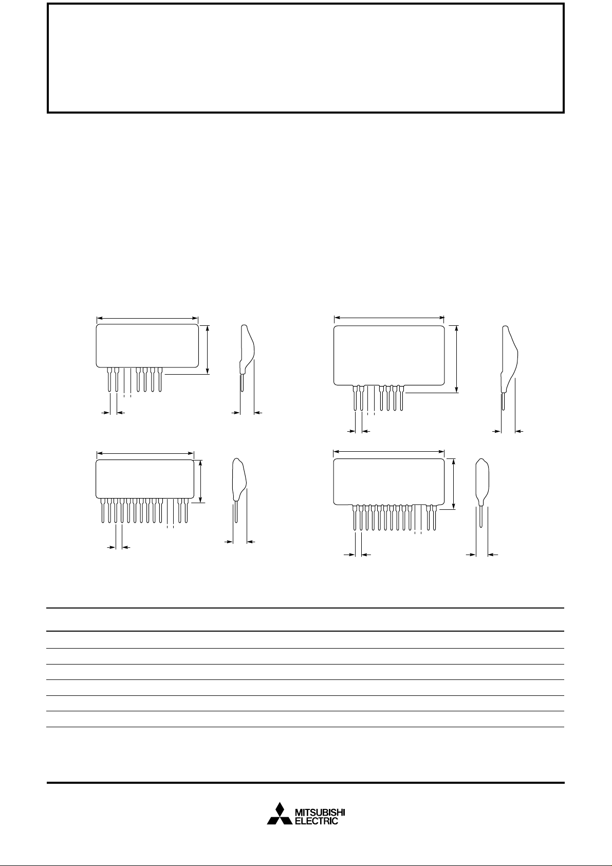
Mitsubishi offers four single in-line
hybrid ICs for driving IGBT
modules. All four drivers are high
speed devices designed to convert
logic level control signals into
optimal IGBT gate drive. Input
signals are isolated from the IGBT
drive using high speed
optocouplers with 15,000V/ms
Figure 5.1 Hybrid IGBT Gate Drivers
35 MAX
M57957L
2.54
23 MAX
10 MAX
common mode noise immunity.
This feature allows convenient
common referencing of high and
low side control signals. Mitsubishi
IGBT drivers are designed to
provide the pulse currents
necessary for high performance
switching applications and to
maintain sufficient off bias to
guarantee ruggedness. Hybrid
IGBT drivers simplify gate drive
M57958L
design by minimizing the number
of components required. In
addition to high performance gate
drive, the M57959L and the
M57962L provide short-circuit
protection. The basic package
outlines of the four Mitsubishi
drivers are shown in Figure 5.1.
Table 5.1 lists the key electrical
characteristics of each hybrid
driver.
51 MAX
29
MAX
10 MAX2.54
43 MAX
M57959L
2.54
All Dimensions in mm.
22 MAX
11 MAX
51 MAX
M57962L
2.54
25
MAX
12 MAX
Table 5.1 Recommended Gate Driver Applications
Optimum Application Range*
Gate Drive Circuit Peak Output Current Short Circuit Protection For 600V IGBT Modules For 1200V/1400V IGBT Modules
M57957L 2 Amps No Up to 100A Up to 50A
M57958L 5 Amps No Up to 400A Up to 200A
M57959L 2 Amps Yes Up to 100A Up to 50A
M57962L 5 Amps Yes Up to 400A Up to 200A
M57958L with Booster** 20 Amps No Up to 600A Up to 1000A
M57962L with Booster** 20 Amps Yes Up to 600A Up to 1000A
*Use RG specified in the switching time section of the IGBT module data sheet.
**See Section 5.10
Sep.1998

MITSUBISHI SEMICONDUCTORS POWER MODULES MOS
USING HYBRID GATE DRIVERS AND GATE DRIVE POWER SUPPLIES
5.1 Output Current Limit
When using hybrid gate drivers
RG must be selected such that the
output current rating (IOP) is not
exceeded. If RG is computed using
Equation 5.1 then IOP will not be
exceeded under any condition.
Equation 5.1
Conservative equation for minimum R
R
G
= (VCC + VEE)/I
G(MIN)
OP
Example:
With VCC = 15V and
-VEE = 10V R
G(MIN)
for
M57958L will be:
RG = (15V + 10V)/5A = 5 ohms
In most applications this limit is
unnecessarily conservative.
Considerably lower values of R
G
can usually be used. The
expression for R
G(MIN)
should be
modified to include the effects of
parasitic inductance in the drive
circuit, IGBT module internal
impedance and the finite switching
speed of the hybrid drivers output
stage. Equation 5.2 is an improved
version of Equation 5.1 for
R
G(MIN)
.
Equation 5.2
Improved equation for R
R
IOP - (RG)
= (VCC + VEE)/
G(MIN)
INT
- φ
G(MIN)
Large IGBT modules that contain
parallel chips have internal gate
resistors that balance the gate
drive and prevent internal
oscillations. The parallel
combination of these internal
resistors is R
G(INT)
. R
G(INT)
ranges from 0.75 ohm in large
IGBT modules like CM600HA-24H
to 3.0 ohms in smaller modules like
CM150DY-12H with two parallel
chips. The value of f depends on
the parasitic inductance of the gate
drive circuit and the switching
speed of the hybrid driver. The
exact value of f is difficult to
determine. It is often desirable to
estimate the minimum value of R
G
that can be used with a given
hybrid driver circuit and IGBT
module by monitoring the peak
gate current while reducing R
G
until the rated IOP is reached. The
minimum restriction on RG often
limits the switching performance
and maximum usable operating frequency when large modules
outside of the drivers optimum
application range are being
driven.Further steps to address
this issue are provided in
Section 5.10.
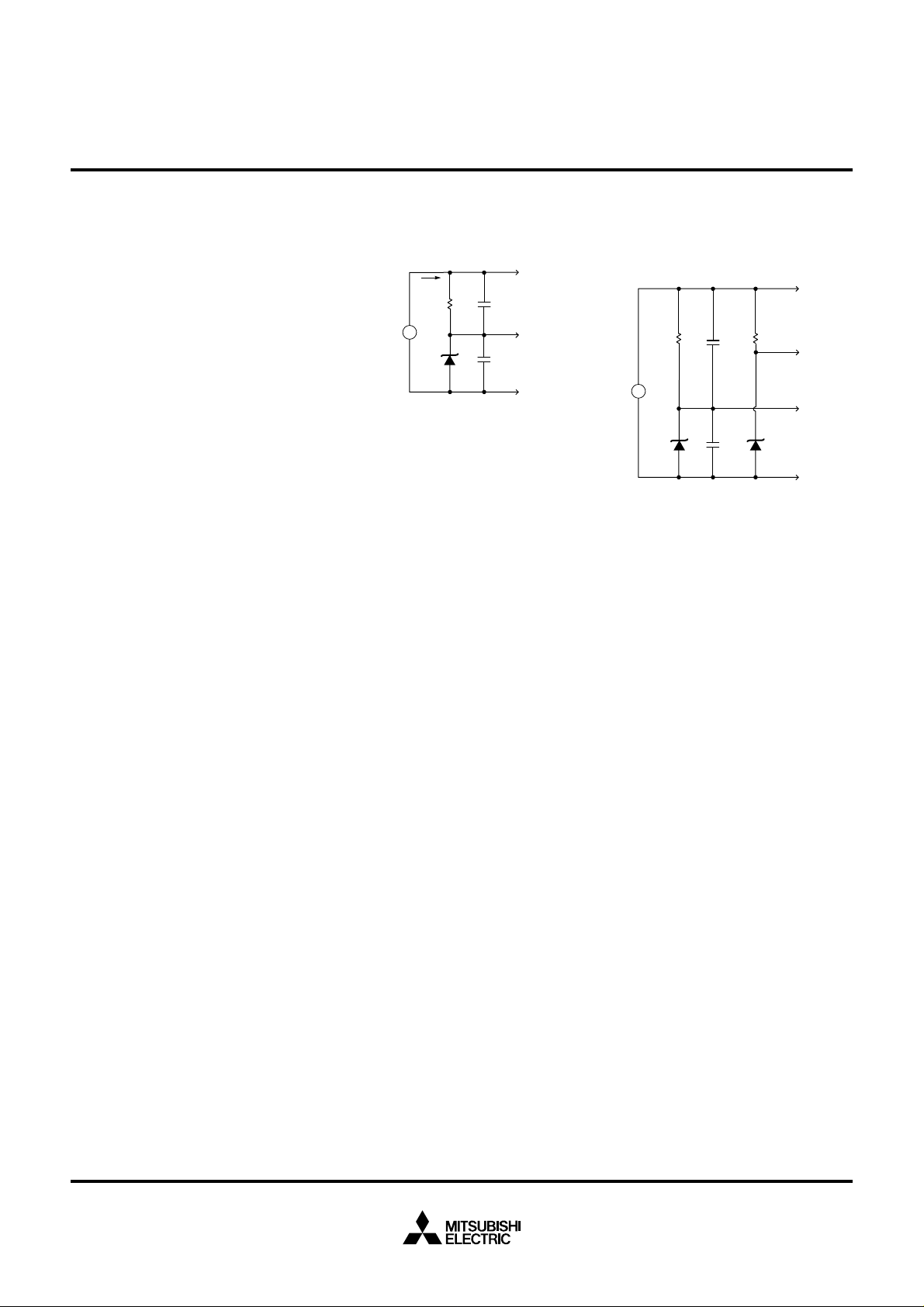
5.2 Power Supply Requirements
Power is usually supplied to hybrid
IGBT gate drivers from low
voltage DC power supplies that
are isolated from the main DC bus
voltage. Isolated power supplies
are required for high side gate
drivers because the emitter
potential of high side IGBTs is
constantly changing. Isolated
power supplies are often desired
for low side IGBT gate drivers in order to eliminate ground loop noise
problems. The gate drive supplies
should have an isolation voltage
rating of at least two times the
IGBTs V
V
= 2400V for 1200V IGBT).
ISO
rating (i.e.
CES
In systems with several isolated
supplies intersupply capacitances
must be minimized in order to
avoid coupling of common mode
Figure 5.2 Hybrid Driver Power
Supply
I
D
V
(15V)
V
(10V)
+
CC
+
EE
I
COM
+
47µF
+
47µF
I
D
TO HYBRID DRIVER
noise. The recommended power
supply configuration for Mitsubishi
hybrid IGBT gate drivers is shown
in Figure 5.2. Two supplies are
used in order to provide the onand off-bias for the IGBT. The recommended on bias supply (VCC)
voltage is +15V and the recommended off-bias supply voltage
(VEE) is -10V.
Normally these supplies should be
regulated to ±10% however
operation within the range
indicated on the individual driver
data sheets is acceptable.
Electrolytic or tantalum decoupling
capacitors should be connected at
the power supply input pins of the
hybrid driver. These capacitors
supply the high pulse currents
required to drive the IGBT gate.
The amount of capacitance
required depends on the size of the
IGBT module being driven. A 47µF
capacitor is sufficient for most applications.
5.2.1 Supply Current
The current that must be supplied
to the IGBT driver is the sum of two
components. One component is
the quiescent current required to
bias the drivers internal circuits.
The current is constant for fixed
values of VCC and VEE. The second component is the current re-
Sep.1998
MITSUBISHI SEMICONDUCTORS POWER MODULES MOS
USING HYBRID GATE DRIVERS AND GATE DRIVE POWER SUPPLIES
quired to drive the IGBT gate. This
current is directly proportional to
the operating frequency and the total gate charge (QG) of the IGBT
being driven. With small IGBT
modules and at low operating frequencies the quiescent current will
be the dominant component. The
amount of current that must be
supplied to the hybrid driver when
VCC = 15V and VEE = -10V can
be determined from Equations 5.3
and 5.4.
Equation 5.3
Required supply current for
M57957L and M57958L
ID = QG x f
PWM
+ 13mA
Equation 5.4
Required supply current for
M57959L and M57962L
ID = QG x f
PWM
+ 18mA
Where:
ID = Required supply current
QG = Gate charge (See
Section 4.6.3)
f
= Operating frequency
PWM
5.2.2 Single Supply Operation
The current drawn from VCC (ID+)
is nearly equal to the current drawn
from VEE (ID-). Only a small
amount of current flows in the common connection (I
COM
). In many
applications it is desirable to operate the hybrid driver from a single
isolated supply. An easy method of
accomplishing this is to create the
common potential using a resistor
and a zener diode. In order to size
the resistor for minimum loss we
must first determine the current
flowing in the common connection
Figure 5.3 Single Supply
Operation of Hybrid
IGBT Drivers
I
D
2.7kΩ
+
V
D
(25V)
(I
). In M57957L and M57958L
COM
10V
+
47µF
+
47µF
TO HYBRID DRIVER
a common connection current of
about 2.5mA is required to bias internal circuits. In M57959L and
M57962L about 3.5mA flows from
the detect pin through the IGBT to
the common connection. The circuit in Figure 5.3 uses a zener supply designed for about 5mA to supply the common current. This circuit allows operation of Mitsubishi
hybrid drivers from a single isolated
25 volt DC supply.
When the power supply circuit
shown in Figure 5.3 is used with
M57957L and M57958L the
required bias voltage at pin 5 of the
hybrid driver appears after a delay
caused by the 2.7kΩ resistor and
the 47µF capacitor. This delay may
cause these drivers to generate an
ON output pulse during power up.
In applications where the main
DC bus voltage is applied before
the gate drive power supplies are
on and stabilized the circuit in Figure 5.4 should be used.
The voltage of the single supply
and the zener diode can be varied
to allow use of standard supplies.
For example, if a 24V DC-to-DC
Figure 5.4 Improved Power
Supply Circuit for
M57957L and
M57958L
TO
HYBRID
DRIVER
2.7kΩ
10V
PIN 6
TO
HYBRID
DRIVER
PIN 5
TO
EMITTER
OF IGBT
TO
HYBRID
DRIVER
PIN 8
V
(25V)
10V
+
47µF
+
47µF
2.7kΩ
+
D
converter is to be used then a 9V
zener diode would give +15/-9
which is acceptable for all of the
hybrid gate drivers. The two
limiting factors that need to be
observed if changes are made are:
(1) Voltages must be within the al-
lowable range specified on the
gate driver data sheet and
(2) The turn on supply should be
15V+/-10% for proper IGBT
performance.
5.3 Total Power Dissipation
The hybrid IGBT driver has a
maximum allowable power
dissipation that is a function of the
ambient temperature. With
VCC = 15V and VEE = -10V the
power dissipated in the driver can
be estimated using Equation 5.5.
Sep.1998

MITSUBISHI SEMICONDUCTORS POWER MODULES MOS
USING HYBRID GATE DRIVERS AND GATE DRIVE POWER SUPPLIES
Equation 5.5
Total power Dissipation
PD = ID x (VCC + VEE)
The power computed using
Equation 5.5 can then be
compared to the derating curves
shown in Figures 5.5 through
5.8 to determine the maximum
allowable ambient temperature.
The power computed using
Equation 5.5 includes the
dissipation in the external gate
resistor (RG). This loss is outside
the hybrid driver and can be
subtracted from the result of
Equation 5.5. The dissipation in
RG is difficult to estimate because
it depends on drive circuit parasitic
inductance, IGBT module type
and the hybrid driver’s switching
speed. In most applications the
loss in RG can be ignored. Direct
use of Equation 5 will result in a
conservative design with the
included loss of RG acting as a
safety margin. When operating
large modules at high frequencies
the limitations on ambient
temperature may be significant.
5.4 Application Circuit for
M57957L and M57958L
An internal schematic and example
application circuit for the M57957L
and M57958L are shown in
Figures 5.9 and 5.10. For
optimum performance parasitic
inductance in the gate drive loop
must be minimized. This is
accomplished by connecting the
47µF decoupling capacitors as
close as possible to the pins of the
hybrid driver and by minimizing the
lead length between the drive
circuit and the IGBT. The zeners
shown should be rated at about 18
volts and be connected as close to
the IGBT’s gate as possible. These
zeners protect the gate during
switching and short circuit
operation.
The gate driver has a built in
185 ohm input resistor that is
designed to provide proper drive
for the internal opto isolator when
V
= 5V. If other input voltages are
IN
desired an external resistor should
be added to maintain the proper
opto drive current of 16ma. The
value of the required external resistor can be computed by assuming
the forward voltage drop of the
opto diode is 2V. For example:
5.5 Short-Circuit Protection
Using Desaturation
Techniques
The M57959L and M57962L have
built in circuits that will protect the
IGBT from short circuits by
detecting desaturation. When a
short circuit occurs a high current
will flow in the IGBT causing its collector to emitter voltage to increase
to a level much higher than normal.
The hybrid driver detects this condition and quickly turns the IGBT
off, saving it from certain destruction.
If 15V drive is required then
R
16ma - 185Ω = 630Ω.
= (15V - 2V) ÷
ext
Sep.1998

MITSUBISHI SEMICONDUCTORS POWER MODULES MOS
USING HYBRID GATE DRIVERS AND GATE DRIVE POWER SUPPLIES
Figure 5.5 Derating Curve for
M57957L
5
4
3
2
1
ALLOWABLE POWER DISSIPATION (W)
0
0 100
20 40 60 80
AMBIENT TEMPERATURE (oC)
Figure 5.7 Derating Curve for
M57959L
5
4
3
2
1
ALLOWABLE POWER DISSIPATION (W)
0
0 100
20 40 60 80
AMBIENT TEMPERATURE (oC)
Figure 5.6 Derating Curve for
M57958L
5
4
3
2
1
ALLOWABLE POWER DISSIPATION (W)
0
0 100
20 40 60 80
AMBIENT TEMPERATURE (oC)
Figure 5.8 Derating Curve for
M57962L
5
4
3
2
1
ALLOWABLE POWER DISSIPATION (W)
0
0 100
20 40 60 80
AMBIENT TEMPERATURE (oC)
5.6 Operation of M57959L
and M57962L
Figure 5.11 is a flow diagram showing the operation of the short protection in M57959L and M57962L.
The hybrid driver monitors the collector emitter voltage (VCE) of the
IGBT. Normally, when an on signal
is applied to the input of the driver
the IGBT will turn on and VCE will
quickly attain its low on-state value
of VCE(SAT). If a short circuit is
present when the on signal is applied a large current will flow in the
IGBT and VCE will remain high. A
short circuit is detected by the hybrid driver when VCE remains
greater than the desaturation trip
level (VSC) for longer than t
TRIP
after the input on signal is applied.
The t
delay is used to avoid
TRIP
false tripping by allowing enough
time for normal turn on of the IGBT.
The hybrid driver initiates a controlled slow turn off and generates
a fault output signal when a short
circuit is detected. The slow turn off
helps to control dangerous transient voltages that can occur when
high short circuit currents are interrupted. The output of the driver will
remain disabled and the fault signal
will remain active for t
RESET
after a
short circuit is detected. The input
signal of the driver must be in its off
state in order for the fault signal to
be reset.
Sep.1998

MITSUBISHI SEMICONDUCTORS POWER MODULES MOS
USING HYBRID GATE DRIVERS AND GATE DRIVE POWER SUPPLIES
Figure 5.9 Internal Schematic Diagram of M57957L and M57958L
5
2
1
6
7
8
Figure 5.10 Application Circuit for M57957L and M57958L
V
LOGIC
SIGNAL
INPUT
BUFFER
IN
2
M57957L
M57958L
1
7
6
+
47µF
5
+
47µF
8
R
G
+
V
CC
+
V
EE
18V
Figure 5.11 Protection Circuit
Operation
START
IS V
CE
GREATER THAN
V
SC
IS
INPUT SIGNAL
ON?
DELAY
t
TRIP
IS VCE
GREATER THAN
V
SC
NO
YES
NO
YES
NO
YES
SLOW SHUTDOWN
DISABLE OUTPUT
SET FAULT SIGNAL
WAIT t
RESET
IS
INPUT SIGNAL
OFF?
YES
CLEAR FAULT
SIGNAL
ENABLE OUTPUT
NO
Sep.1998

MITSUBISHI SEMICONDUCTORS POWER MODULES MOS
USING HYBRID GATE DRIVERS AND GATE DRIVE POWER SUPPLIES
5.7 Application Circuit for
M57959L and M57962L
Figure 5.12 is a block diagram of
the M57959L and M57962L drivers
showing the logical implementation
of the flow diagram in Figure 5.11.
Figure 5.13 is an example application circuit for M57959L and
M57962L. Parasitic inductance in
the drive circuit should be minimized using the techniques described for the M57957L and
M57958L in Section 5.4. Pins
(3,7,9,10) are used for factory testing and should not be connected to
any external circuit. The detect diode (D1) must be fast recovery
(approximately 100ns) and should
be rated at a voltage equal to or
higher than the IGBT module being
driven. The 20V zener DZ1 is recommended in order to protect the
hybrid IC’s detect input from transient voltages that can occur during
recovery of the detect diode. This
zener can be eliminated if the detect diode’s recovery remains fast
and soft over its entire temperature
range and pin 1 of the hybrid IC remains free of high voltage transients and ringing.
tor can be computed by assuming
5.8 Adjusting the Desaturation
the forward voltage drop of the
opto diode is 2V. For example:
The hybrid drivers built in t
If 15V drive is required then
delay will work for most
applications. However when large
R
= (15V - 2V) ÷
ext
16ma - 185Ω = 630Ω.
modules are being driven with near
maximum gate resistance the
driver may incorrectly detect a
Figure 5.12 Block Diagram for M57959L
DETECT
V
CC
COMPARE
V
ISOLATION
TRIP
FAULT
LATCH
QSQS
R
DISABLE OUTPUT
FAULT
INPUT
V
CC
V
EE
Trip Time (t
DELAY
t
TRIP
ONE
SHOT
t
RESET
AND
TRIP
AND
GATE DRIVE
)
SHORT
DETECTED
SLOW
SHUTDOWN
TRIP
GATE
The gate driver has a built in
185 ohm input resistor that is
designed to provide proper drive
for the internal opto isolator when
V
= 5V. If other input voltages are
IN
desired an external resistor should
be added to maintain the proper
opto drive current of 16mA. The
value of the required external resis-
Figure 5.13 Block Diagram for M57959L
FAULT
LOGIC
SIGNAL
INPUT
OUTPUT
Buffer
V
IN
14
M57959L
M57962L
13
4.7 kΩ
8
1
5
4
6
Sources for D1: EDI (Electronic Devices Inc.) P/N RF160A
VMI (Voltage Multipliers Inc.) P/N 1N6528
+
47µF
+
47µF
DZ1 30V
D1
R
G
+
V
CC
+
V
EE
18V
Sep.1998

MITSUBISHI SEMICONDUCTORS POWER MODULES MOS
USING HYBRID GATE DRIVERS AND GATE DRIVE POWER SUPPLIES
short circuit. The false trip occurs
because it takes longer than
t
for the module to reach its
TRIP
low on-state voltage. In these
applications the t
TRIP
delay can
be extended by connecting a
capacitor from pin 2 to VCC.
Figure 5.14 shows the typical
increase in t
as a function of
TRIP
the external capacitor value for
M57959L and M57962L.
5.9 Operational Waveforms
Figure 5.15 is a typical waveform
showing the gate to emitter
voltage during a slow shutdown for
M57962L. Approximately 2.4ms
after the detect input (pin 1)
voltage exceeds VSC the gate to
emitter voltage is slowly brought to
zero in about 2ms. Figure 5.16
shows the collector-emitter voltage
(VCE) and collector current (IC) for
an IGBT module during a short
circuit. This waveform shows the
effectiveness of the slow shutdown
in controlling transient voltage.
5.10 Driving Large IGBT
Modules
In order to achieve efficient and
reliable operation of high current,
high voltage IGBT modules, a
gate driver with high pulse
current capability and low output
impedance is required. Mitsubishi
hybrid gate drivers are designed to
perform this function as stand
alone units in most applications.
However, for optimum performance
with large modules, it may be
necessary to add an output booster
stage to the hybrid gate driver.
When using the hybrid gate drivers
as stand alone units with IGBT
modules outside the range
specified in Table 5.1, three things
must be considered. First, the
maximum peak output current
rating of the hybrid gate driver
places a restriction on the
minimum value of RG that can be
used. For example, the minimum
allowable RG for M57962L is about
5 ohms (for additional information
refer to Section 5.1). This value is
higher than the recommended
value for many large IGBTs. Using
RG larger than the data sheet
value will cause an increase in
t
, t
d(on)
, tr and turn-on
d(off)
switching losses. In high frequency
(more than 5kHz) applications
these additional losses are usually
unacceptable. Second, even if the
additional losses and slower
switching times are acceptable, the
drivers allowable power dissipation
must be considered. At an ambient
temperature of 60°C, the M57962L
is permitted to dissipate a
maximum of about 1.5Ω (for more
information refer to Section 5.3). If
a CM600HA-24H is being used, the
driver will dissipate 1.5W at a
switching frequency of 14kHz. In
this case, operation at a higher frequency than 14kHz will cause the
driver to overheat. Lastly, the
driver’s slow shutdown becomes
less effective when it is used with
large devices. This occurs because
current that flows to the gate
through the relatively high reverse
transfer capacitance (C
res
) of
large devices can not be absorbed
by the driver. Its output impedance
is not low enough. The slow
shutdown may become less
slow and a larger turn-off snubber
capacitor may be required. This
third limitation is perhaps the most
serious. In some cases, the hybrid
driver may completely lose control
of the gate voltage and allow it to
Figure 5.14 Adding
Capacitance to
Extend t
7
6
, (µs)
5
TRIP
4
3
2
DESATURATION TRIP TIME t
1
0
0 15000
CONDITIONS:
V
CC
5000
CAPACITANCE (pF)
Figure 5.15 VGE and V
TRIP
M57962L
M57959L
= 15V, VEE,= -10V, TC= 25°C
10000
DETECT
Waveform
V
GE
V
DETECT
0
CONDITIONS:
VCC= 15V, VEE= -10V, TC= 25
VGE: 5v/div, V
DETECT
: 5v/div, 1µs/div
Figure 5.16 Short-Circuit
Shutdown
Waveform
CONDITIONS:
= 300V, Tj= 25°C
V
BUS
0
: 50v/div, IC: 100A/
V
CE
V
CE
, 0.5µs/div
div
I
C
°C
Sep.1998

MITSUBISHI SEMICONDUCTORS POWER MODULES MOS
USING HYBRID GATE DRIVERS AND GATE DRIVE POWER SUPPLIES
climb above 15V. If this happens,
the short circuit durability of the
IGBT module may be compromised.
All of the limitations outlined
above can be overcome by adding
a discrete npn/pnp complimentary
output stage to the hybrid driver.
One possible implementation is
shown in Figure 5.18.
The NPN and PNP booster
transistors should be fast switching
(tf < 200nS) and have sufficient
current gain to deliver the desired
peak output current. Table 5.2
lists some combinations of booster
transistors that can be used in
the circuit shown in figure 5.18.
Normally, either M57958L or
M57962L is used to drive the
booster stage. However, if the
gain of the booster transistors is
sufficiently high the lower current
M57957L and M57959L can be
used. If very high gain or
Darlington type transistors are
used in the booster stage care
must be exercised to avoid
oscillations in the output stage. It
may become necessary to add
resistance from base to emitter on
the booster transistors as shown in
Figure 5.19. In addition, when
darlingtons are used the turn-on
supply may need to be increased in
order to compensate for the
additional voltage drop across the
booster stage.
Figure 5.17 shows an example
output waveform with a
booster constructed using
D44VH10/D45VH10. For this
example, an output impedance
of 1ohm was used to drive a
capacitive load of 300nF. The
circuit shown in Figure 5.18 shows
the output booster being used with
M57962L. This output booster
stage can be used with M57958L
if short circuit protection is not
needed.
Figure 5.17 Output Waveform,
I
= 5A/div,
OUT
V
= 5V /div,
OUT
T = 1µs/div
V
OUT
I
OUT
M2
M 1.00µs ch3 -5.4V
Figure 5.18 Example Circuit for Driving Large IGBT Modules
FAULT
OUTPUT
VIN=5V
LOGIC
SIGNAL
INPUT
BUFFER
4.7 kΩ
8
V
IN
14
M57962L
13
1
5
4
6
DZ1
30V
+
47µF
+
47µF
VCC=15V VEE=10V
D1
+
V
CC
+
V
EE
EDI: RF160A
VMI: 1N6528
R
G
IGBT
MODULE
Sep.1998

MITSUBISHI SEMICONDUCTORS POWER MODULES MOS
USING HYBRID GATE DRIVERS AND GATE DRIVE POWER SUPPLIES
Table 5.2 Booster Stage Transistors
npn Transistor pnp Transistor Peak Current V
MJD44H11 MJD45H11 15A 80V Motorola Surface Mount
D44VH10 D45VH10 20A 80V Motorola TO-220
MJE15030 MJE15031 15A 150V Motorola TO-220
MJE243 MJE253 8A 100V Motorola TO-255
2SC4151 2SA1601 30A 40V Shindengen Isolated TO-220
Figure 5.19 Alternate Booster Stage Configuration
PIN 5 OF M57962L OR
PIN 7 OF M57958L
R
G
TO IGBT
GATE
CEO
Manufacturer Package
Sep.1998
 Loading...