

Page 1
MITSUBISHI <CONTROL / DRIVER IC>
)
M56789FP
4 CHANNEL ACTUATOR DRIVER
DESCRIPTION
The M56789FP is a semiconductor integrated circuit in order to
drive 4ch actuator.
FEATURES
●Large power dissipation (Power Package).
●3.3V DSP available.
●Low saturation voltage (typical 0.6V at load current 500mA).
●Low cross-over distortion.
●Wide supply voltage range.(4.5V–13.2V)
●Divided Motor power supplies into three parts.
●Ch1, Ch2 and Ch3 can be controlled by PWM.
●Ch1 and Ch2 can act in the Current Control mode.
●Two naked Operational Amplifiers.
●TSD(Thermal Shut Down) circuit.
●Two mute circuits.
APPLICATION
CD-ROM, DVD, DVD-ROM etc.
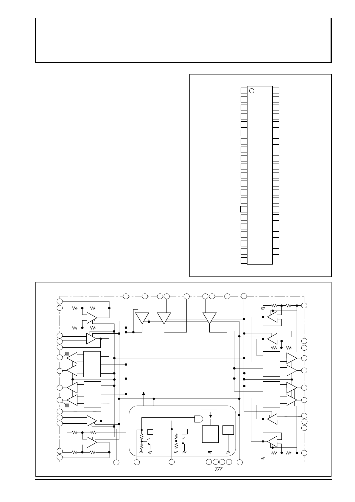
PIN CONFIGURATION(TOP VIEW
MUTE2
MUTE1
SOUT2
SIN2-
IN2+
IN2-
GND
OUT2
VM2-
VM2+
GND
VM1+
VM1-
OUT1
IN1-
IN1+
Vm1
SIN1-
SOUT1
CC1
V
OP2OUT
1
2
3
4
7
8
13
14
15 28
16
17
18 25
19
20
21
42
41
40
39
385
376
36
35
M56789FP
349
3310
3211
3112
30
29
27
26
24
23
22
CC2
V
VREF
VREFO
IN3IN3+
Vm3
OUT3
VM3VM3+
GND
VM4+
VM4IN4AGND
Vm2
IN4BOP1OUT
OP1-
OP1+
OP2+
OP2-
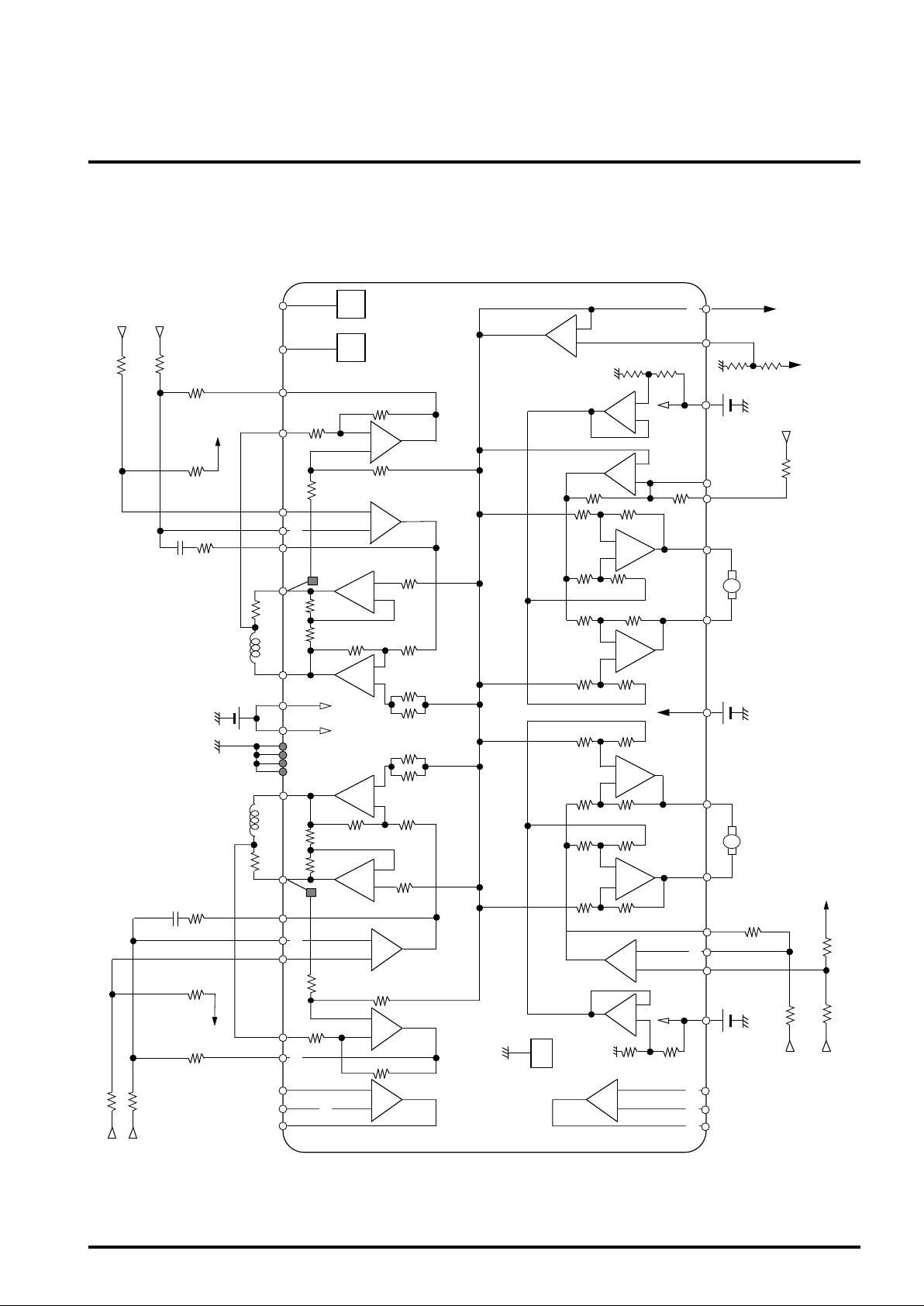
BLOCK DIAGRAM
SOUT1
19
SIN1-
18
IN1+
16
IN1-
15
14
OUT1
VM1(+)
VM1(-)
VM2(-)
VM2(+)
OUT2
IN2-
IN2+
SIN2-
SOUT2
+
12
-
-
13
+
+
9
-
-
10
+
8
6
5
4
3
-
+
+
A3
-
CH1
CH2
A3
+
+
A3
-
E1
E2
S2
S1
Vm1
VREFO
MUTE1
OP2+
VREF
4140 21
-
+
A2
BIAS
2
OP2-
23
22
-
+
A4
OP2
1ch
2ch
3ch
1 7 111729 33
MUTE2
OP2
OUT
VCC2
VREFO
CC1
V
OP1+
4ch
OP1-
-
+
A4A3
OP1
Hi:Sleep
SLEEP
GND (4PINS)
OP1
OUT
262524
TSD
20
CC1
V
Outline 42P9R-B
V
CC2
42
E4
CH4
CH3
E3
A1
A3
A1
A1
Vm2
28
+
-
+
-
+
-
+
+
-
+
-
+
+
27
30
32
31
35
34
39
38
36
37
IN4BIN4A-
VM4(+)
VM4(-)
VM3(-)
VM3(+)
IN3IN3+
OUT3
Vm3
Page 2
PIN DESCRIPTIONS
Pin No.
1
2
3
4
5
6
8
9
10
, 11
7
12
13
14
15
16
17
18
19
20
21 22
Symbol Symbol
MUTE2
MUTE1
SOUT2
SIN2IN2+
IN2OUT2
VM2(-)
VM2(+)
GND
VM1(+)
VM1(-)
OUT1
IN1IN1+
Vm1
SIN1-
SOUT1
V
CC1
OP2OUT
CH4 mute
CH1,2 and 3 mute
S2 amplifier output
S2 amplifier inverted input
E2 amplifier non-inverted input
E2 amplifier inverted input
E2 amplifier output
CH2 inverted output
CH2 non-inverted output
GND
CH1 non-inverted output
CH1 inverted output
E1 amplifier output
E1 amplifier inverted input
E1 amplifier non-inverted input
Motor power supply - 1
S1 amplifier inverted input
S1 amplifier output
5V power supply
OP2 amplifier output OP2 amplifier inverted input
Function Pin No. Function
MITSUBISHI <CONTROL / DRIVER IC>
M56789FP
4 CHANNEL ACTUATOR DRIVER
42
41
40
39
38
37
36
35
34
, 33
29
32
31
30
28
27
26
25
24
23
V
CC2
VREF
VREFO
IN3IN3+
Vm3
OUT3
VM3(-)
VM3(+)
GND
VM4(+)
VM4(-)
IN4AVm2
IN4BOP1OUT
OP1OP1+
OP2+
OP2-
Bootstrap power supply
Reference voltage input
Reference voltage output
E3 amplifier inverted input
E3 amplifier non-inverted input
Motor power supply - 3
E3 amplifier output
CH3 inverted output
CH3 non-inverted output
GND
CH4 non-inverted output
CH4 inverted output
E4 amplifier low gain input
Motor power supply - 2
E4 amplifier high gain input
OP1 amplifier output
OP1 amplifier inverted input
OP1 amplifier non-inverted input
OP2 amplifier non-inverted input
ABSOLUTE MAXIMUM RATING (Ta=25˚C )
Symbol
V
CC2 Bootstrap power supply
Vm Motor power supply
V
CC1 5V power supply
Io Output Current
Vin1
Vin2
Pt Power dissipation Free Air
Kθ
Tj Junction temperature
Topr
Tstg
Parameter Conditions Rating Unit
42 pin input voltage
17 , 28 and 37 pins input voltage
20 pin input voltage
Maximum input voltage
of terminals
Thermal derating
1 , 2 , 5 , 6 , 15 , 16 , 22 , 23 , 24 , 25 , 27 , 30 , 38 , 39 , 41 pins
4 , 18 pins
Free Air
Operating temperature
Storage temperature
RECOMMENDED OPERATING CONDITIONS
Symbol Parameter
CC1 4.5 5.0 5.5
VCC2
5V power supplyV
Bootstrap power supply
Min. Typ. Max.
Limits
Vm + 1.0
15
15
7.0
700
0 – VCC1
0 – Vm1
1.2 W
9.6
150
-20 – +75
-40 – +150
V
V
V
mA
V
mW / ˚C
˚C
˚C
˚C
Unit
V
V
V5.0Vm1, 2, 3 Motor power supply-1, 2, 3
Page 3
MITSUBISHI <CONTROL / DRIVER IC>
M56789FP
4 CHANNEL ACTUATOR DRIVER
ELECTRICAL CHARACTERISTICS
(Ta=25˚C, VCC1=Vm1=Vm2=Vm3=5V,VCC2=12V, no-load current unless otherwise noted.)
Symbol Parameter
CC1 Supply current - 1 , , , pins supply current ( Vref=Vctl=2.5V)
I
ICC2 Supply current - 2 pin[VCC1] supply current ( Vref=Vctl=2.5V)
CC3
I
Sleep Mode Supply
current - 3
17 28 37 42
20
, , , , pins supply current (MUTE1,2=H)
17 20 28 37 42
Conditions
Min.
VsatCH1 Ch1 Saturation voltage
VsatCH2
VsatCH3
VsatCH4
Ch2 Saturation voltage
Ch3 Saturation voltage
Ch4 Saturation voltage
Top and Bottom saturation voltage.
Load current 500mA. At bootstrap.
Vmute-on Mute-on voltage Mute-on 2.0
Vmute-off Mute-off voltage Mute-off
Imute and pin input current at 5V input voltage. 170 250
VinOP 0.5
VoutOP 0.5
VofOP
Mute terminals input current
OP1 and OP2 amplifier
Input voltage range
OP1 and OP2 amplifier
output voltage range
OP1 and OP2 amplifier
input offset voltage
OP1 and OP2 amplifier
input current
OP1 and OP2 amplifier
input current offset
GBOP 2.3 4
VinE 0.5 VCC2-2.0 V
VoutE 1.0
VofE
IinE
IofE
VoutS
VinVREF 2.51.5 V
VofVREF
OP1 and OP2 amplifier GB
E1,E2 and E3 amplifier
Input voltage range
E1,E2 and E3 amplifier
output voltage range
E1,E2 and E3 amplifier
input offset voltage
E1,E2 and E3 amplifier
input current
E1,E2 and E3 amplifier
input current offset
S1 and S2 amplifier
output voltage range
VREF buffer amplifier
Input voltage range
VREF buffer amplifier
offset voltage
1 2
Io= 2.0mA
Vin = 2.5V(at buffer )
inverted input = non-inverted input =2.5V
inverted input = non-inverted input =2.5V
-10 +10 mV
-1.0 0 µAIinOP -0.15
-100 +100 nAIofOP 0
No load
Vin = 2.5V(at buffer )
inverted input = non-inverted input =2.5V
inverted input = non-inverted input =2.5V
-10
-1.0 0 µA-0.15
-100 +100 nA0
No load 1.0 V
41
-10
VREFO = OUT1 = 2.5V
VofCH1 Ch1 output offset voltage
when the OUT1 voltage is adjusted at the
-26
same VREFO voltage, at VREF= 2.5V
VREFO = OUT2 = 2.5V
VofCH2 Ch2 output offset voltage
when the OUT2 voltage is adjusted at the
same VREFO voltage, at VREF= 2.5V
VREFO = OUT3 = 2.5V
VofCH3 Ch3 output offset voltage
when the OUT3 voltage is adjusted at the
-26
same VREFO voltage, at VREF= 2.5V
VREFO = IN4A- = 2.5V
VofCH4 Ch4 output offset voltage
when the IN4A- voltage is adjusted at the same
-26
VREFO voltage, at VREF= 2.5V
VofS1
VofS2
S1 output offset voltage
S2 output offset voltage
SOUT1-VREFO (at SI N1[-] = VM1[+] )
at VREF = 2.5V
SOUT2-VREFO (at SI N2[-] = VM2[+] )
at VREF = 2.5V
-20
-20
Limits
Typ.
Max.
24 36 mA
9.5 15 mA
500 µA
0.85 1.28 V
0.85 V
1.28
0.6 0.9 V
0.7 1.0 V
0.8
VCC2-1.0
VCC1-0.5
VCC1-0.5 V
+10 mV
CC1-0.5 V
CC1-1.2 V
+10
+26
+26
+26
+26
+20
+20
Unit
V
V
µA
V
V
MHz
mVpin input voltage = 2.5V
mV
mV-26
mV
mV
mV
mV
Page 4
MITSUBISHI <CONTROL / DRIVER IC>
4 CHANNEL ACTUATOR DRIVER
ELECTRICAL CHARACTERISTICS
(Ta=25˚C, VCC1=Vm1=Vm2=Vm3=5V,VCC2=12V, no-load current unless otherwise noted.)
Symbol Parameter Conditions
GainCH1 14
GainCH2 14
GainCH3
GainCH4
GainS1
Ch1 power amplifier
voltage gain
Ch2 power amplifier
voltage gain
Ch3 power amplifier
voltage gain
Ch4 power amplifier
voltage gain
S1 amplifier voltage gain
S2 amplifier voltage gain
{VM1(+)–VM1(-)}
( OUT1 – VREFO)
{VM2(+) – VM2(-)}
( OUT2 – VREFO)
{VM3(+) – VM3(-)}
( OUT3 – VREFO)
-1• {VM4(+) – VM4(-)}
(I N4A[-]–VREFO)
{SOUT1 - VREFO}
(VM1[+] - SI N1[-] )
{SOUT2 - VREFO}
(VM2[+] - SI N2[-] )
at VREF=2.5V
at VREF=2.5V
at VREF=2.5V
at VREF=2.5V
at VREF=2.5V
at VREF=2.5V
Min.
3.17 4.91
Limits
Typ. Max.
4.08 dB
6.02
6.02
M56789FP
Unit
dB13.1 14.8
dB13.1 14.8
20.819.1
6.855.11
6.855.11
dB20
dB
dBGainS2
INPUT and OUTPUT CHARACTERISTICS of EACH CHANNELS
<INPUT>
VREFO
<OUTPUT>
VREFO
<INPUT>
VREFO
<OUTPUT>
VREFO
2.5V
2.5V
CH1 amplifier
CH2 amplifier
41
40
16
15
14
41
40
5
6
8
GainCH2
VREF
VREFO
IN1+
IN1-
OUT1
GainCH1
VREF
VREFO
IN2+
IN2OUT2
Output of non-inverted Amp.
(Gain = X2.5)
+
-
E1
+
-
+
-
+
-
CH1
Output of inverted Amp.
(Gain = X-2.5)
Differential voltage gain = 5
Output of non-inverted Amp.
(Gain = X2.5)
E2
Output of inverted Amp.
(Gain = X-2.5)
CH2
+
12
-
+
13
-
+
-
+
-
Differential voltage gain = 5
VM1+
VM1-
10
9
VM2+
VM2-
0.5V
0.5V
0.2V
0.2V
0.5V
0.5V
VM1+
VM2+
OUT1
VM1-
OUT2
VM2-
Page 5
MITSUBISHI <CONTROL / DRIVER IC>
M56789FP
4 CHANNEL ACTUATOR DRIVER
2.5V
2.5V
2.5V
CH3 amplifier
CH4 amplifier
IN4BIN4A-
Vctl4
GainCH4
VREF
41
VREFO
40
38
IN3+
39
IN3-
36
OUT3
GainCH3
VREF
41
VREFO
40
E4
27
30
25K
(Gain = X-0.16)
Output of non-inverted Amp.
(Gain = X5)
+
CH3
E3
+
-
Output of inverted Amp.
(Gain = X-5)
+
34
-
+
35
-
Differential voltage gain = 10
Output of non-inverted Amp.
(Gain = X5)
+
CH4
+
-
Output of inverted Amp.
4K
(Gain = X-5)
+
32
-
+
31
-
Differential voltage gain = 1.6
VM3+
VM3-
VM4+
VM4-
<INPUT>
VREFO
<OUTPUT>
Vrefm3
(Vm3/2)
<INPUT>
VREFO
<OUTPUT>
Vrefm4
(Vm4/2)
1.0V
0.8V
0.2V
1.0V
1.0V
0.8V
VM3+
VM4-
OUT3
VM3-
Vctl4
VM4+
Page 6

MITSUBISHI <CONTROL / DRIVER IC>
M56789FP
4 CHANNEL ACTUATOR DRIVER
S1 amplifier
SIN1-
18
VM1+
12
S2 amplifier
SIN2-
4
VM2+
10
5K 10K
+
5K
5K
5K
10K
GainS1
+
10K
19
40
Voltage gain = 2
10K
3
40
SOUT1
VREFO
SOUT2
VREFO
<INPUT>
VM1+
<OUTPUT>
VREFO
<INPUT>
VM2+
<OUTPUT>
SIN1-
0.5V
SOUT1
1.0V
SIN2-
0.5V
SOUT2
Voltage gain = 2GainS2
VREFO
1.0V
Page 7

I/O terminal equivalent circuit
(1)VREF amplifier I/O terminal equivalent circuit
(VREF, VREFO)
MITSUBISHI <CONTROL / DRIVER IC>
M56789FP
4 CHANNEL ACTUATOR DRIVER
(2)E1,E2,E3 amplifier I/O terminal equivalent circuit
(IN1+, IN1-, OUT1, IN2+, IN2-, OUT2, IN3+, IN3-, OUT3)
VCC1
VREFO
GND
GND V
VREF
CC1
GND
VCC1
VREFO
(3)E4 amplifier I/O terminal equivalent circuit
(IN4A-, IN4B-)
VREFO
VCC2
VCC1
GND
V
IN-
GND
CC1
V
IN+ OUT
GND VCC1
CC1
(4)OP1, OP2 amplifier I/O terminal equivalent circuit
(OP1+, OP1-, OP1OUT, OP2+, OP2-, OP2OUT)
VCC2
VCC1
VCC2
VCC1
GND V
IN4B-
CC1
GND
IN4A-
CC1
V
(5)S1,S2 amplifier I/O terminal equivalent circuit
(SIN1-, SOUT1, SIN2-, SOUT2)
VM(+)
5K
GND Vm1
SIN-
5K
10K
10K
GND
GND
SOUT
VREFO
VCC2
CC1
V
CC1
V
GND V
OP-
CC1
GND
V
CC1
OP+ OPOUT
(6)MUTE circuits equivalent circuit
(MUTE1, MUTE2)
MUTE
GND VCC1
VCC1
25K
23K
GND
GND
GND
V
CC1
Page 8

MITSUBISHI <CONTROL / DRIVER IC>
M56789FP
4 CHANNEL ACTUATOR DRIVER
I/O terminal equivalent circuit
(7)CH1,2,3,4 power amplifier
OUTPUT terminal equivalent circuit
(VM1(+), VM1(-), VM2(+), VM2(-),
VM3(+), VM3(-), VM4(+), VM4(-), )
VCC2
Vm
VM(+,-)
GND
BASICALLY CHARACTERISTIC S
Output saturation voltage and Load current characteristic.
This data is an example for typical sample.
BOOTSTRAP
The equivalent circuits of an output stage of the power amplifier
are shown in (7) .
The power supplies of CH1,CH2 are Vm1.
The power supply of CH3 is Vm3, and the power supply of CH4 is
Vm2.
The source side of the power amplifier output stage consists of a
PNP and a NPN. The emitta of the PNP is connected to VCC2. So
the power supplies of the PNP can be adjusted externally.
[About bootstrap advantage]
The output stage of the power amplifier consists of the preceding
components. If VCC2 is provided with higher voltage input than
Vm* (The recommendation voltage is Vm*+1V) externally, the
output range can be wider than that of VCC2=Vm*.
Please take advantage of this bootstrap function for the system
which has many power supplies. And it is the same with the
external bootstrap circuit which provides VCC2 with higher voltage
inputs than Vm*.
Also the bootstrap can decrease the saturation voltage at the
source side of the power amplifier output stage. Therefore, when
the outputs of the power amplifiers which drive motors and
actuators are fully swung, the power dissipation of the IC will be
decreased.
CH1
5.0
4.0
3.0
2.0
Output Voltage (V)
1.0
0
CH3
5.0
4.0
3.0
2.0
Output Voltage (V)
1.0
0
Vm1=VCC1=5v,VCC2=12v
0.3v
0.5v
0.2 0.4 0.5
Load Current (mA)
Vm3=VCC1=5v,VCC2=12v
0.22v
0.24v
0.2 0.4 0.5 0.6 0.8 1.0
Load Current (mA)
VM3+,VM3-
VM1+,VM1-
0.35v
0.6 0.8 1.0
VM3+,VM3-
VM1+
VM1-
0.46v
0.5v
CH2
5.0
4.0
3.0
2.0
Output Voltage (V)
1.0
0
CH4
5.0
4.0
3.0
2.0
Output Voltage (V)
1.0
0
Vm1=VCC1=5v,VCC2=12v
0.3v
0.5v
0.2 0.4 0.5 0.6 0.8 1.0
Load Current (mA)
Vm2=VCC1=5v,VCC2=12v
0.3v
0.3v
0.2 0.4 0.5 0.6 0.8 1.0
Load Current (mA)
VM2+,VM2-
0.3v
VM4+,VM4-
VM4+,VM4-
VM2+
VM2-
0.6v
0.6v
Page 9

NON-BOOTSTRAP
MITSUBISHI <CONTROL / DRIVER IC>
M56789FP
4 CHANNEL ACTUATOR DRIVER
CH1
5.0
4.0
3.0
2.0
Output Voltage (V)
1.0
0
5.0
4.0
3.0
2.0
Output Voltage (V)
1.0
Vm1=VCC1=VCC2=5v
VM1+,VM1-
1.0v
0.5v
0.2 0.4 0.5 0.6 0.8 1.0
Load Current (mA)
CH3
1.0v
0.24v
0.35v
Vm3=VCC1=VCC2=5v
VM4+,VM4-
VM3+,VM3-
VM1+
VM1-
0.5v
CH2
5.0
4.0
3.0
2.0
Output Voltage (V)
1.0
0
CH4
5.0
4.0
3.0
2.0
Output Voltage (V)
1.0
Vm1=VCC1=VCC2=5v
VM2+,VM2-
1.0v
0.5v
0.2 0.4 0.5 0.6 0.8 1.0
Load Current (mA)
Vm2=VCC1=VCC2=5v
1.0v
0.3v
0.3v
VM4+,VM4-
VM4+,VM4-
VM2+
VM2-
0.6v
0
0.2 0.4 0.5 0.6 0.8 1.0
Load Current (mA)
THERMAL DERATING
6.0
(W)
5.0
4.0
3.0
2.0
Power Dissipation (Pdp)
1.0
0 25 50 75 100 125 150
Ambient Temperature Ta (˚C)
3.6W using N-type board
2.6W using P-type board
0
0.2 0.4 0.5 0.6 0.8 1.0
Load Current (mA)
This IC's package is POWER-SSOP, so improving the board on
which the IC is mounted enables a large power dissipation without
a heat sink.
For example, using an 1 layer glass epoxy resin board, the IC's
power dissipation is 2.6W at least. And it comes to 3.6W by using
an improved 2 layer board.
The information of the N, P type board is shown in the board
information.
Page 10

APPLICATION CIRCUIT No.1
* single input (linear signal)
* Direct voltage control
MITSUBISHI <CONTROL / DRIVER IC>
M56789FP
4 CHANNEL ACTUATOR DRIVER
VCTL1
cf.R1=10K,R2=14K
Voltage gain=GainCH1•R2/R1
if.Ra=10
Current gain=7/10=0.7(A/V)
=5•14/10
=7(V/V)=16.9dB
R2R1
FOCUS TRACKING
5V
VREFO
VCTL2
VREFO
Ra
MUTE2
MUTE1
SIN1-SOUT1
IN1+ IN2+
IN1-
OUT1
VM1+ VM1-
GND
VM2+VM2-
OUT2
IN2-
SIN2-
SOUT2
5K
10K
10K
5K
5K
10K
5K
OP1+
OP1-
12.5K
Vm1
VCC1
12.5K 5K10K
ch4
ch1,
ch2, ch3
10K
+-
10K
+-
+-
+-
+-
-
+
-
+
10K
+
-
10K
+
-
5K
5K
12.5K
5K
12.5K
5K
5K
OP1OUT
TSD
OP2OUT
+-
4K
+
-
+-
12.5K2.5K
+
12.5K2.5K
12.5K2.5K
+-
12.5K2.5K
12.5K2.5K
+
-
12.5K2.5K
12.5K2.5K
+-
12.5K2.5K
-
+
-
+
+
-
VREF0
2.5V
VREF
10K10K
Vm2
5V
IN4B-
IN4A-
25K
VM4+ VM4-
M
VCC2
12V
VM3- VM3+
M
OUT3
IN3-
VREFO
Vm3IN3+
5V
10K10K
OP2+
OP2-
VCTL4
TRAY
TRAVERSE
VCTL3
Page 11

APPLICATION CIRCUIT No.2
* single input (linear signal)
* Direct current control (for FOCUS and TRACKING)
MITSUBISHI <CONTROL / DRIVER IC>
M56789FP
4 CHANNEL ACTUATOR DRIVER
cf.R1=10K,R2=14K,Rs=1
Current gain=R2 / [R1•GainS1•Rs]
R1
=14 / [10•2•1]
=0.7(A/V)
*Phase compensation filter
VCTL2
VCTL1
FOCUS TRACKING
R2
5V
VREFO
Rs
Ra
VREFO
MUTE2
MUTE1
SIN1-SOUT1
IN1+ IN2+
IN1-
OUT1
VM1+ VM1-
GND
VM2+VM2-
OUT2
IN2-
SIN2-
SOUT2
5K
5K
5K
10K
10K
10K
5K
OP1+
OP1-
Vm1
VCC1
12.5K 5K10K
12.5K
ch4
ch1,
ch2, ch3
10K
+-
10K
+-
+-
+
+-
+
-
+
10K
+
-
10K
+
-
S1
E1
5K
5K
12.5K
5K
12.5K
5K
5K
OP1OUT
TSD
OP2OUT
+-
4K
+
-
+-
12.5K2.5K
-
+
12.5K2.5K
12.5K2.5K
+
12.5K2.5K
12.5K2.5K
+
-
12.5K2.5K
12.5K2.5K
+-
12.5K2.5K
+
+
+
-
VREF0
2.5V
VREF
10K10K
Vm2
5V
IN4B-
IN4A-
25K
VM4+ VM4-
M
VCC2
12V
VM3- VM3+
M
OUT3
IN3-
VREFO
Vm3IN3+
5V
10K10K
OP2+
OP2-
VCTL4
TRAY
TRAVERSE
VCTL3
Page 12

APPLICATION CIRCUIT No.3
* Differential PWM input (for FOCUS,TRACKING and TRAVERSE)
* Direct voltage control
MITSUBISHI <CONTROL / DRIVER IC>
M56789FP
4 CHANNEL ACTUATOR DRIVER
C2
C1
PWM2
VREFO
VREFO
R3
PWM2
R2
R4
R1R1
R3
PWM1
PWM1
R2
C1
FOCUS TRACKING
5V
C2
R4
MUTE2
MUTE1
SIN1-SOUT1
IN1+
IN1-
OUT1
VM1+ VM1-
GND
VM2+VM2-
OUT2
IN2-
IN2+
SIN2-
SOUT2
5K
10K
10K
5K
5K
10K
5K
OP1+
OP1-
12.5K
Vm1
VCC1
12.5K 5K10K
ch4
ch1,
ch2, ch3
10K
+-
10K
+-
+-
+-
+-
+
+
10K
+
-
10K
+
-
5K
5K
12.5K
5K
12.5K
5K
5K
OP1OUT
TSD
OP2OUT
+-
+
-
+-
4K
12.5K2.5K
+ +
12.5K2.5K
12.5K2.5K
-
12.5K2.5K
12.5K2.5K
+
-
12.5K2.5K
12.5K2.5K
+-
12.5K2.5K
+
+
+
-
10K10K
10K10K
VREF
25K
VM4+ VM4-
VCC2
VM3- VM3+
OUT3
IN3-
Vm3IN3+
OP2+ OP2-
VREF0
Vm2
IN4B-
IN4A-
5V
2.5V
5V
M
12V
M
VCTL4
TRAY
TRAVERSE
C3
R6
R5
PWM1
R6
R5
VREFO
C3
PWM2
Page 13

APPLICATION CIRCUIT No.4
* Differential PWM input (for FOCUS,TRACKING and TRAVERSE)
* Direct current control (for FOCUS and TRACKING)
PWM1
R3
R1
PWM2
R3
R1
C2
C2
R2
VREFO
C1
R2
C1
FOCUS TRACKING
VREFO
R4
R4
5V
MUTE2
MUTE1
SIN1-SOUT1
IN1+ IN2+
IN1-
OUT1
VM1+ VM1-
GND
VM2+VM2-
OUT2
IN2-
SIN2-
SOUT2
5K
5K
5K
10K
10K
10K
5K
OP1+
OP1-
Vm1
VCC1
12.5K
12.5K 5K10K
PA
ch4
ch1,
ch2, ch3
10K
+-
10K
+-
+-
+-
+-
+
-
+
10K
+
-
10K
+
-
5K
5K
12.5K
5K
12.5K
5K
5K
OP1OUT
MITSUBISHI <CONTROL / DRIVER IC>
M56789FP
4 CHANNEL ACTUATOR DRIVER
VREF0
OP1
TSD
OP2OUT
+-
4K
+
-
+-
12.5K2.5K
-
+
12.5K2.5K
12.5K2.5K
+
12.5K2.5K
12.5K2.5K
+
-
12.5K2.5K
12.5K2.5K
+-
12.5K2.5K
+
+
+
-
10K10K
25K
10K10K
2.5V
VREF
Vm2
5V
IN4B-
IN4A-
VM4+ VM4-
M
VCC2
12V
VM3- VM3+
M
OUT3
IN3-
Vm3IN3+
5V
OP2+ OP2-
VCTL4
TRAY
TRAVERSE
C3
R6
R5
PWM1
VREFO
R6
R5
PWM2
C3
PWM2
PWM1
Page 14

APPLICATION CIRCUIT No.5 (for 3.3V DSP)
* single input (linear signal)
* Direct voltage control
MITSUBISHI <CONTROL / DRIVER IC>
M56789FP
4 CHANNEL ACTUATOR DRIVER
R3
REF
R1R1
R2
VREFO
VREFO
R4
REF
R3
VCTL1
VCTL2
R2
FOCUS TRACKING
5V
R4
MUTE2
MUTE1
5K
SIN1-SOUT1
IN1+ IN2+
IN1-
OUT1
VM1+ VM1-
GND
VM2+VM2-
OUT2
IN2-
SIN2-
SOUT2
5K
5K
10K
10K
10K
5K
OP1+
OP1-
12.5K
Vm1
VCC1
12.5K 5K10K
ch4
ch1,
ch2, ch3
10K
+-
10K
+-
+-
+
+-
+
+
10K
+
-
10K
+
-
5K
5K
12.5K
5K
12.5K
5K
5K
OP1OUT
TSD
OP2OUT
+-
+-
4K
12.5K2.5K
+ +
12.5K2.5K
12.5K2.5K
-
12.5K2.5K
12.5K2.5K
+
-
12.5K2.5K
12.5K2.5K
+-
12.5K2.5K
+
-
+
-
+
+
10K10K
10K10K
VREF0
VREF
Vm2
IN4B-
IN4A-
25K
VM4+ VM4-
VCC2
VM3- VM3+
OUT3
IN3-
Vm3IN3+
OP2+ OP2-
5V
M
12V
M
5V
VREFO
10K10K
VCTL4
TRAY
TRAVERSE
R6
R5
VCTL3
MCU
power
supply
5v
VREFO
R6
R5
REF
Page 15
APPLICATION CIRCUIT No.6 (for 3.3V DSP)
* single input (linear signal)
* Direct current control (for FOCUS and TRACKING)
Vref
1.65V
R1
R3
R3
VCTL1
R1
R2
VREFO
R2
FOCUS TRACKING
VREFO
R4
R4
5V
MUTE2
MUTE1
SIN1-SOUT1
IN1+ IN2+
IN1-
OUT1
VM1+ VM1-
GND
VM2+VM2-
OUT2
IN2-
SIN2-
SOUT2
5K
5K
5K
10K
10K
10K
5K
OP1+
OP1-
Vm1
VCC1
12.5K
12.5K 5K10K
PA
ch4
ch1,
ch2, ch3
10K
+-
10K
+-
+-
+-
+-
+
-
+
10K
+
-
10K
+
-
5K
5K
12.5K
5K
12.5K
5K
5K
OP1OUT
MITSUBISHI <CONTROL / DRIVER IC>
M56789FP
4 CHANNEL ACTUATOR DRIVER
OP1
TSD
OP2OUT
+-
4K
+
-
+-
12.5K2.5K
-
+
12.5K2.5K
12.5K2.5K
+
12.5K2.5K
12.5K2.5K
+
-
12.5K2.5K
12.5K2.5K
+-
12.5K2.5K
+
+
+
-
10K10K
10K10K
VREF0
25K
VM4+ VM4-
OP2+ OP2-
VREF
Vm2
IN4B-
IN4A-
VCC2
VM3- VM3+
OUT3
IN3-
Vm3IN3+
5V
M
12V
M
5V
VREFO
10K10K
VCTL4
TRAY
TRAVERSE
R6
R5
VCTL3
MCU
power
supply
5v
VREFO
R6
R5
Vref
1.65v
Vref
1.65v
VCTL2
 Loading...