

Page 1
MITSUBISHI <CONTROL / DRIVER IC>
)
M56788FP
5 CHANNEL ACTUATOR DRIVER
DESCRIPTION
The M56788FP is a semiconductor integrated circuit in order 5ch
actuator.
FEATURES
● Low saturation voltage.
● 3.3V DSP available.
● There are two motor power supplies.
Vm1 CH1,2 motor power supply-1
Vm2 CH3,4,5 motor power supply-2
● Built-in OP amp. for Regulator.
(It enables a Regulator which consists of external PNP Tr.s and
resistors.)
● Flexible Input amp. setting.(It enables PWM control.)
● Low cross-over distortion.(4.5V–13.2V)
● Wide supply voltage range.(4.5V–13.2V)
● Built-in Thermal Shut Down circuit.
● Built-in Mute circuit.(two systems)
MUTE1:CH1–4, MUTE2:CH5
APPLICATION
MD, CD-audio, CD-ROM, VCD,DVD etc.
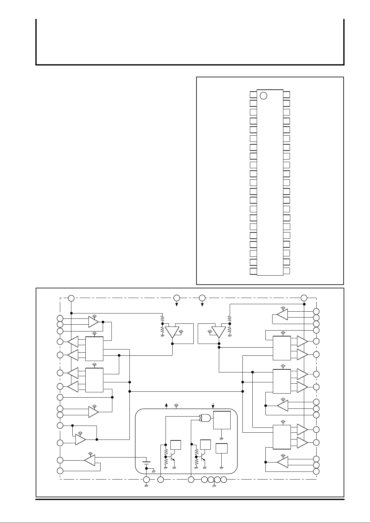
PIN CONFIGURATION(TOP VIEW
CH3IN
1
OUT3
2
IN3-
3
VBS2
4
Vm2
N.C
GND
7
IN3+
8
VM3-
VM3+
GND
VM4+
VM4-
13
VM5+
14
VM5-
15 28
OUT5
16
IN5-
17
IN5+
18 25
IN4+
19
IN4-
20
OUT4
21
Outline 42P9R-B
M56788FP
42
41
40
39
385
376
36
35
349
3310
3211
3112
30
29
27
26
24
23
22
REG+
REGB
IN1+
VBS1
Vm1
IN1OUT1
VM1VM1+
GND
VM2+
VM2OUT2
GND
IN2IN2+
MUTE1
MUTE2
SS.GND
VREF
VREFO
N.C: no connection
IN1+
IN1-
OUT1
VM1(+)
VM1(-)
VM2(+)
VM2(-)
OUT2
IN2-
IN2+
VREFO
VREF
REGB
REG+
Vm1
38
40
37
36
+
34
-
-
35
+
+
32
-
-
31
+
30
28
27
22
+
23
VBS2
41
VREG
42
+
-
+
VBS1
VREF
CH1
x5
CH2
x5
-
+
VBS1
E1
VBS1
VBS1
VBS1
E2
1.25v
SS.GND
R
R
Vrefm1
BIAS
MUTE1
VBS1
39 4
+
Vm1 Vm2
-
VBS1
Low,Open
MUTE ON
1–4
CH
252624
MUTE2
VBS2
Hi:Sleep
5CH
7
GND(4PINS)
+
-
Vrefm2
VREFO
SLEEP
TSD
2911
33
Vm2
5
VBS2
-
VBS2
VBS2
VBS2
E4
VBS2
VBS2
E5
E3
CH3
x8
CH4
x8
CH5
x8
+
+
-
+
+
-
+
-
+
+
-
+
+
R
R
3
8
2
1
10
9
12
13
20
19
21
14
15
17
18
16
IN3IN3+
OUT3
CH3IN
VM3(+)
VM3(-)
VM4(+)
VM4(-)
IN4IN4+
OUT4
VM5(+)
VM5(-)
IN5IN5+
OUT5
Page 2
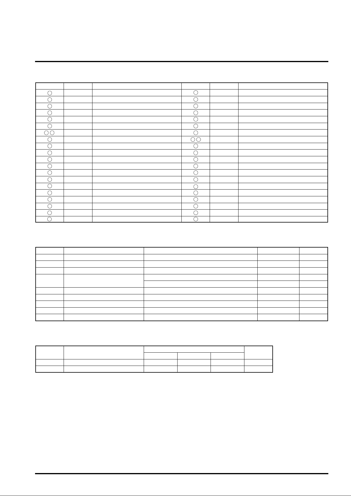
PIN FUNCTION
Symbol SymbolTerminal Terminal function Terminal Terminal function
1
2
3
4
5
6
7 , 11
8
9 30
10 31
12
13 34
14
15
16
17 38
18 39
19
20 41
21 42
CH3IN
OUT3
IN3-
VBS2
Vm2
N.C N.C
GND Motor GND
IN3+ E3 amplifier non-inverted input
VM3(-) CH3 inverted output
VM3(+) CH3 non-inverted output
VM4(+) CH4 non-inverted output
VM4(-) CH4 inverted output
VM5(+) CH5 non-inverted output
VM5(-) CH5 inverted output
OUT5 E5 amplifier output
IN5- E5 amplifier inverted input
IN5+ E5 amplifier non-inverted input
IN4+ E4 amplifier non-inverted input
IN4- E4 amplifier inverted input
OUT4 E4 amplifier output
CH3 non-inverted input
E3 amplifier output
E3 amplifier inverted input
Bootstrap power supply
Motor power supply
22
23
24
25
26
27
28
29 , 33
32
35
36
37
40
MITSUBISHI <CONTROL / DRIVER IC>
M56788FP
5 CHANNEL ACTUATOR DRIVER
VREF0
VREF
SS.GND
GND Motor GND
VBS1 Bootstrap power supply
REGB Regulator PNP base connect
REG+ Regulator voltage setting resistor
Reference voltage output
Reference voltage input
Small signal GND
CH5 mute MUTE2
CH1–4 mute MUTE1
E2 amplifier non-inverted inputIN2+
E2 amplifier inverted inputIN2-
E2 amplifier outputOUT2
CH2 inverted outputVM2(-)
CH2 non-inverted outputVM2(+)
CH1 non-inverted outputVM1(+)
CH1 inverted outputVM1(-)
E1 amplifier outputOUT1
E1 amplifier inverted inputIN1Motor power supplyVm1
E1 amplifier non-inverted inputIN1+
ABSOLUTE MAXIMUM RATING (Ta=25˚C )
Symbol Parameter Conditions Rating Units
VBS
Vm
Io
Vin
Pt
Kq
Tj
Topr
Tstg
Bootstrap power supply
Motor power supply
Output Current
Maximum input voltage of terminals
Power dissipation
Thermal derating
Junction temperature
Operating temperature
Storage temperature
VBS power supply
Vm power supply
23, 25, 26, 27, 28, 37, 40PIN
1, 3, 8, 17, 18, 19, 20, 42PIN
Free Air
Free Air
15
15
500
0–VBS1
0–VBS2
1.2
9.6
150
-20–+75
-40–+150
RECOMMENDED OPERATING CONDITIONS
Symbol
Vm1,Vm2
Motor power supply
Parameter
VBS1,VBS2 Bootstrap power supply
Min
Limits
Typ Max
5.0
Vm*+1.0
Units
V
V
V
V
mA
V
V
W
mW/˚C
˚C
˚C
˚C
Page 3
MITSUBISHI <CONTROL / DRIVER IC>
M56788FP
5 CHANNEL ACTUATOR DRIVER
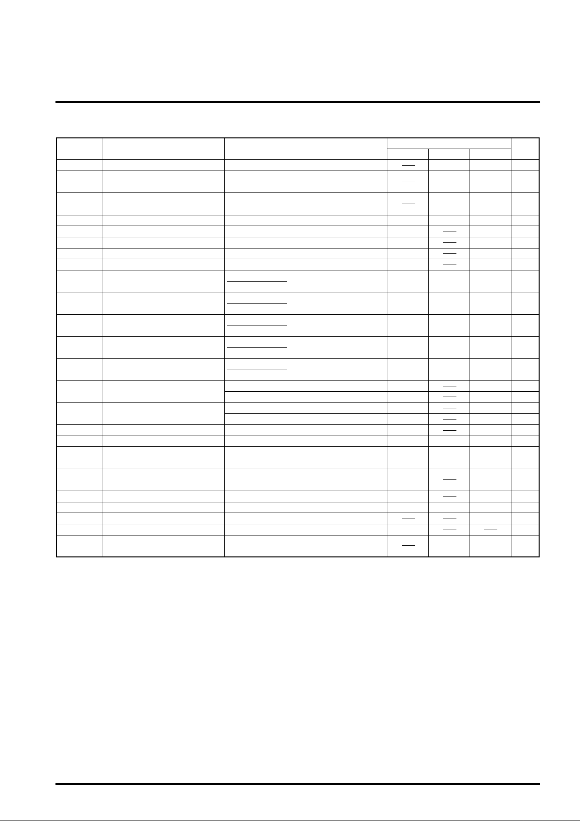
ELECTRICAL CHARACTERISTICS (Ta=25˚C, VBS=Vm=5V unless otherwise noted.)
Symbol Parameter Conditions
Icc1 Supply current-1 VBS1,VBS2,Vm1,Vm2 current 35 50 mA
Icc2 Supply current-2
Vsat1 CH1–5 Saturation voltage
Voff1 CH1 output offset voltage
Voff2 CH2 output offset voltage
Voff3 CH3 output offset voltage
Voff4 CH4 output offset voltage
Voff5 CH5 output offset voltage
Gain1
Gain2
Gain3
Gain4
Gain5
VinE
VoutE
VofE
IinE
Reg-out
VinVREF
VofVREF
IinVREF
Vmute-on
Vmute-off
Imute
CH1 Voltage Gain between input
and output
CH2 Voltage Gain between input
and output
CH3 Voltage Gain between input
and output
CH4 Voltage Gain between input
and output
CH5 Voltage Gain between input
and output
E1,2,3,4,5 amplifier input voltage
range
E1,2,3,4,5 amplifier output
voltage range
E1,2,3,4,5 amplifier offset voltage
E1,2,3,4,5 amplifier input current
Regulator output voltage range
VREF amplifier input voltage
range
VREF amplifier offset voltage Vin=1.5V ±2mA load
VREF amplifier input current VREF=1.5V
Mute-on voltage Mute-on
Mute-off voltage
Mute terminal input current
VBS1,VBS2,Vm1,Vm2 current at Sleep Mode
(MUTE 1=MUTE 2=0V).
Top and Bottom saturation voltage.
Load current 0.5A and no bootstrap.
VREFO=OUT1=1.5V
VREFO=OUT2=1.5V
VREFO=CH3IN=1.5V
VREFO=OUT4=1.5V
VREFO=OUT5=1.5V
{VM1(+)–VM1(-)}
(OUT1–VREFO)
{VM2(+)–VM2(-)}
(OUT2–VREFO)
{VM3(+)–VM3(-)}
(CH3IN–VREFO)
{VM4(+)–VM4(-)}
(OUT4–VREFO)
{VM5(+)–VM5(-)}
(OUT5–VREFO)
E1,E2 amp
E3,E4,E5 amp
E1,E2 amp(no load)
E3,E4,E5 amp(no load)
Vin = 1.5V(at buffer )
IN+=IN-=1.5V
At VBS=7.5V, Regulator voltage setting
resistor 10K/30K, connects external PNP.
Mute-off
Mute terminal input current(at 5V input
voltage)
Min
-41
-41
-47
-47
-47
4.5
4.5
7.2
7.2
7.2
0.5
0.5
0.5
0.5
-10
-1.0
4.8
1.0
-10
-1.0
2.0
Limits
Typ Max
1.3 2.2 mA
1.35 1.9 V
41 mV
47
47
47
5
5
8
8
8
-0.05
5.0
-0.05
170
5.5
5.5
8.8
8.8
8.8
VBS1-2.0
VBS2-2.0
VBS1-0.5
VBS2-0.5
+10
0
5.2
VBS1-2.0
+10
0
0.8
250
Units
mV41
mV
mV
mV
V/V
V/V
V/V
V/V
V/V
V
V
V
V
mV
µA
V
V
mV
µA
V
V
µA
Page 4

MITSUBISHI <CONTROL / DRIVER IC>
M56788FP
5 CHANNEL ACTUATOR DRIVER
MUTE Function
M56788FP has 2 MUTE terminals and the functions are as follows.
MUTE 1
26 pin
High High ENABLE ENABLE ENABLE ENABLE
Low/Open
High
Low/Open
When both MUTE1 inputs and MUTE 2 inputs are low voltage or open, the IC is in Sleep Mode.
INPUT and OUTPUT CHARACTER I STICS of EACH CHANNELS
CH1,2
1.5V
Reference 1.5V
Low/Open
Low/Open
VREFO
VREF
OUT
IN-
IN+
MUTE 2
25 pin
High
Power and Control Amp.
circuits of CH1 to CH4.
DISABLE
ENABLE
DISABLE
Vm1
-
r
+
Vrefm1 Amp.
r
-
+
Vref Amp.
-
+
Input Amp.
Vrefm1
R 2.5R
+
-
R 2.5R
R 2.5R
+
-
R 2.5R
Power and Control Amp.
circuits of CH5.
ENABLE ENABLE
DISABLE
DISABLE DISABLE
<INPUT>
1.5V
VM+
<OUTPUT>
VM-
Vrefm1
(Vm/2)
Gain=x5
VREF Amp. VREG Amp.
ENABLE
OUT
0.2V
VM+
0.5V
0.5V
ENABLE
ENABLE
ENABLE
VM-
CH3
1.5V
OPOUT
Reference 1.5V
CH4,5
1.5V
Reference 1.5V
VREFO
VREF
CH3IN
OP-
OP+
VREFO
VREF
OUT
IN-
IN+
Vm2
r
+
r
Vrefm2 Amp.
-
+
Vref Amp.
-
+
OP Amp.
Vm2
r
+
Vrefm2 Amp.
r
-
+
Vref Amp.
-
+
Input Amp.
<INPUT>
-
R4R
R4R
R4R
R4R
+
+
-
-
Vrefm2
VM3+
VM3-
Gain=x8
1.5V
<OUTPUT>
Vrefm2
(Vm/2)
0.2V
0.8V
0.8V
<INPUT>
-
R4R
R4R
R4R
R4R
+
+
-
-
Vrefm2
VM+
VM-
Gain=x8
1.5V
<OUTPUT>
Vrefm2
(Vm/2)
0.2V
0.8V
0.8V
CH3IN
VM3+
OUT
VM+
VM3-
VM-
Page 5

I/O terminal Equivalent circuit
(1)E1, E2 input amplifier
I/O terminal equivalent circuit
(IN1+, IN1-, OUT1, IN2+, IN2-, OUT2)
VBS1
MITSUBISHI <CONTROL / DRIVER IC>
M56788FP
5 CHANNEL ACTUATOR DRIVER
(2)E3, E4, E5 input amplifier
I/O terminal equivalent circuit
(IN3+, IN3-, OUT3, IN4+, IN4-, OUT4, IN5+, IN5-, OUT5)
VBS2
E3 amplifier
isn't include.
GND VBS1
IN*-
GND VBS1 GND VBS1
IN*+ OUT*
(3)VREF amplifier I/O terminal
equivalent circuit
(VREF, VREFO)
GND VBS1
VREF
(5)CH3IN input terminal equivalent circuit
Please refer to the application circuits.
(It shows the circuitry of the IC.)
VBS1
GND VBS1
VREFO
GND VBS2
IN*-
(3)VREG amplifier I/O terminal
equivalent circuit
(REG+, REGB)
2K
GND VBS2
REG+
(3)MUTE equivalent circuit
(MUTE1, MUTE2)
MUTE*
GND VBS1
GND VBS2 GND VBS2
IN*+ OUT*
VBS2
1.25V
9.5K
GND VBS2
REGB
GND VBS2
CH3IN
2K
23K
23K
GND
Page 6

I/O terminal equivalent circuit
(7)CH1,CH2 power I/O terminal equivalent circuit
(VM1(+), VM1(-), VM2(+), VM2(-))
VBS1
Vm1
VM
GND
(8)CH3,CH4,CH5 power amplifier output terminal equivalent circuit
(VM3(+), VM3(-), VM4(+), VM4(-), VM5(+), VM5(-))
VBS2
Vm2
VM
GND
MITSUBISHI <CONTROL / DRIVER IC>
M56788FP
5 CHANNEL ACTUATOR DRIVER
The equivalent circuits of an output stage of power amplifiers are
shown in(7) and(8) .
The power supplies of CH1, CH2 are Vm1.
And the power supplies of CH3, CH4, CH5 are Vm2.
The source side of the power amplifier output stage consists of a
PNP and a NPN.
In the case of the CH1 and CH2, the emitta of the PNP is
connected to VBS1, and in the case of the CH3, CH4 and CH5, it
is connected to VBS2. So the power supplies of the PNP can be
adjusted externally.
[About bootstrap advantage]
The output stage of the power amplifier consists of the preceding
components. If VBS* is provided with higher voltage input than
Vm*(The recommendationvoltage is Vm*+1V) externally, the
output range can be wider than that of VBS*=Vm*.
Please take advantage of this bootstrap function for the system
which has many power supplies. And it is the same with the
external bootstrap circuit which provides VBS* with higher voltage
inputs than Vm*.
Also the bootstrap can decrease the saturation voltage at the
source side of the power amplifier output stage. Therefore, when
the outputs of the power amplifiers which drive motors and
actuators are fully swung, the power dissipation of the IC will be
decreased.
THERMAL DERATING
6.0
(W)
5.0
4.0
3.0
2.0
Power Dissipation (Pdp)
1.0
0 25 50 75 100 125 150
Ambient Temperature Ta(˚C)
3.6W using N-type board
2.6W using P-type board
This IC's package is POWER-SSOP, so improving the board on
which the IC is mounted enables a large power dissipation without
a heat sink.
For example, using an 1 layer glass epoxy resin board, the IC's
power dissipation is 2.6W at least. And it comes to 3.6W by using
an improved 2 layer board.
The information of the N, P type board is shown in the board
information.
(˚C)
Page 7

MITSUBISHI <CONTROL / DRIVER IC>
5 CHANNEL ACTUATOR DRIVER
APPLICATION CIRCUIT No.1 single input (linear signal)•Direct voltage control
5V
5V
VBS1
VBS2
Vm2
RR
Vrefm2
Vref
VREFO
+
M56788FP
VREFO
1.5V
VREF
VCTL1
VCTL2
3V
SS.GND
VREFO
VREFO
VBS
14K
10K
5V
R1 R2
FOCUS
R3 R4
TRACKING
MUTE1
MUTE2
Ra
Vm1
IN1+
IN1-
OUT1
VM1+
x5
VM1-
IN2+
IN2OUT2
VM2+
x5
VM2-
REGB
REG+
RR
+-+-
+-
+-
+-+-+-+-
+-
1.25V
Vrefm1
E1
x2.5
x2.5
E2
x2.5
x2.5
Reg-amp
1–4CH5CH
SLEEP
Hi:Sleep
TSD
E3
x4
x4
E4
x4
x4
E5
x4
x4
x8
x8
x8
IN3+
IN3-
OUT3
CH3IN
VM3+
VM3-
IN4+
IN4-
OUT4
VM4+
VM4-
IN5+
IN5-
OUT5
VM5+
VM5-
VREFO
R6 R5
SPINDLE SLED ROADING
M
VREFO
R8 R7
M
VREFO
R10 R9
M
VCTL3
VCTL4
VCTL5
+
-
+-
+-
+
-
+-
+-
+
-
+-
+-
SS.GND
GND
(4PINS)
Page 8

MITSUBISHI <CONTROL / DRIVER IC>
M56788FP
5 CHANNEL ACTUATOR DRIVER
APPLICATION CIRCUIT No.2 Differential PWM input • Direct voltage control (FOCUS, TRACKING, SPINDLE,
SLED, ROADING)
C1
R1
VREFO
C2
PWM1
PWM2
R1
R2
VREFO
R4
R2
R4
5V
5V
5V
C1
FOCUS
Ra
VBS1
VBS2
Vm2
Vm1
IN1+
IN1OUT1
VM1+
x5
VM1-
IN2+
IN2OUT2
RR
RR
+-+-
+-
+-
Vrefm2
Vrefm1
E1
x2.5
x2.5
E2
E3
VREFO
VREFO
-
Vref
+
VREF
+
-
x4
x4
+-+-
IN3+
IN3-
OUT3
CH3IN
VM3+
x8
VM3-
1.5V
PWM1
R6
C3
It can be opened at
Propagation
characteristic check.
SPINDLE SLED ROADING
M
PWM1
R5
R6
R7
PWM2
R5
C3
VREFO
PWM2
R7
R3
3V
SS.GND
PWM2
14K
10K
R3
VBS
PWM1
C2
TRACKING
MUTE1
MUTE2
VM2+
x5
VM2-
REGB
REG+
x2.5
+-+-+-+-
x2.5
+-
1.25V
1–4CH5CH
Reg-amp
SLEEP
Hi:Sleep
TSD
E4
x4
x4
E5
x4
x4
x8
x8
IN4+
IN4-
OUT4
VM4+
VM4-
IN5+
IN5-
OUT5
VM5+
VM5-
R8
R10
C4
R8
C4
VREFO
M
VREFO
C5
C5
R9
R9 R10
M
PWM1
PWM2
+
-
+-+-
+
-
+-+-
SS.GND
GND
(4PINS)
 Loading...