

Page 1
MITSUBISHI <CONTROL / DRIVER IC>
)
M56787FP
SPINDLE MOTOR DRIVER
DESCRIPTION
The M56787FP is a semiconductor integrated circuit in order to
drive the spindle motor.
FEATURES
●Low motor echo noise.
●3.3V DSP available.
●Large power dissipation package(Power Package).
●High motor drive current .
●Wide dynamic range.
●Motor current control for both motor torque directions.
●Reverse torque mode select [SHORT BRAKING,etc].
●Sleep mode.
●FG signal output terminal.
●FG pulse select.
●Automatic stop.
APPLICATION
CD-ROM, DVD, DVD-ROM, DVD-RAM etc.
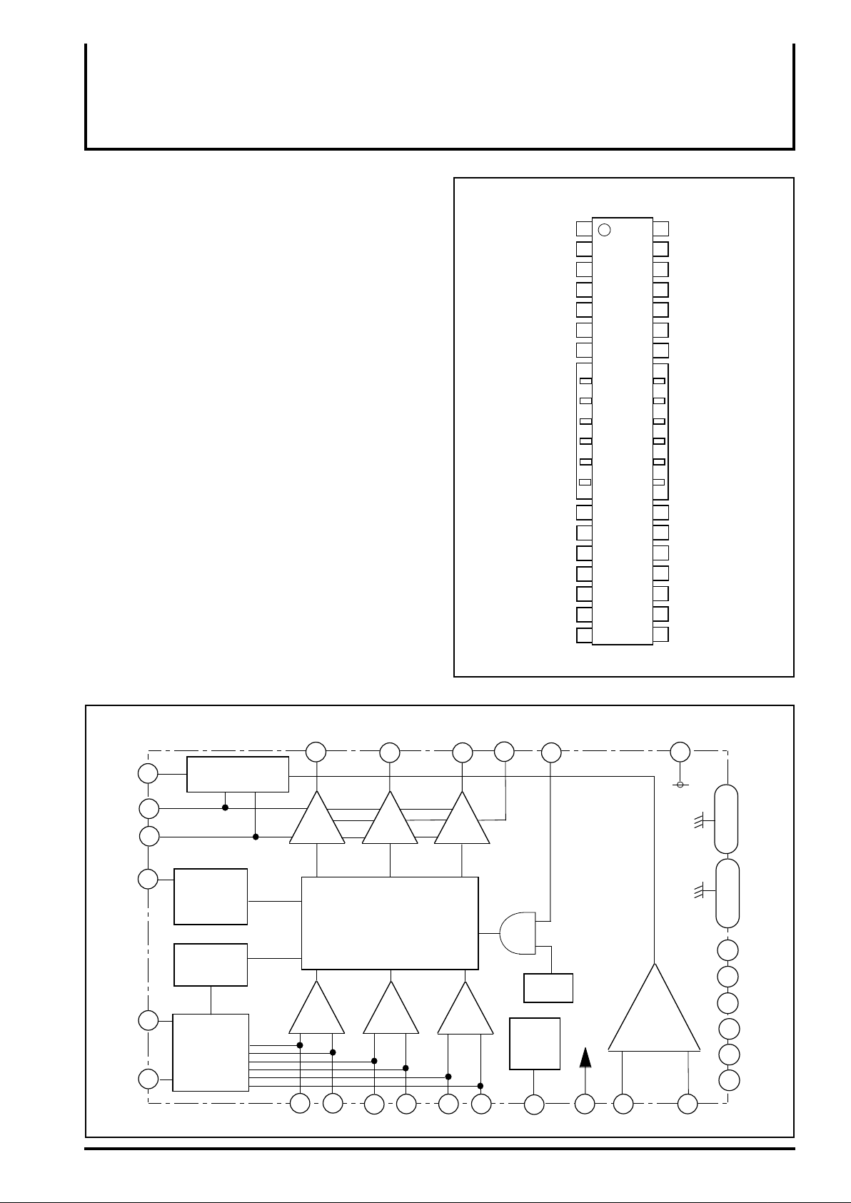
PIN CONFIGURATION(TOP VIEW
N.C
N.C
S/S
FGS
FG
CI
BRS
GND
13
14
R
S
15 28
VCC2
16
17
EC
18 25
ECR
V
CC1
19
HB
20
N.C
21
1
2
3
4
7
8
Outline 42P9R-A
42
41
40
39
385
376
36
35
349
M56787FP
M56787FP
3310
3211
3112
30
29
27
26
24
23
22
N.C
N.C
W
V
U
MGND
TP
GND
HwHw+
HvHv+
Hu-
Hu+
N.C
N.C: no connection
BLOCK DIAGRAM
CI
6
15
RS
16
VCC2
BRS
FG
FGS
7
5
4
BRAKING
MODE
CHANGE
REVERSE
DETECT
FG
&
SELECT
CURRENT
SENSE & LIMIT
U
38 39 40
+
-
23 24 25 26 27 28
V
120˚
MATRIX
+
W
+
-
-
MGND
37
TSD
HALL
BIAS
20
HB
S/S
3
36
TP
VCC1
19
CONTROL
17 18
EC ECRHu+ Hu- Hv+ Hv- Hw+ Hw-
8 to 14
29 to 35
1
2
21
22
41
42
GND
GND
N.C
N.C
N.C
N.C
N.C
N.C
Page 2
MITSUBISHI <CONTROL / DRIVER IC>
M56787FP
SPINDLE MOTOR DRIVER
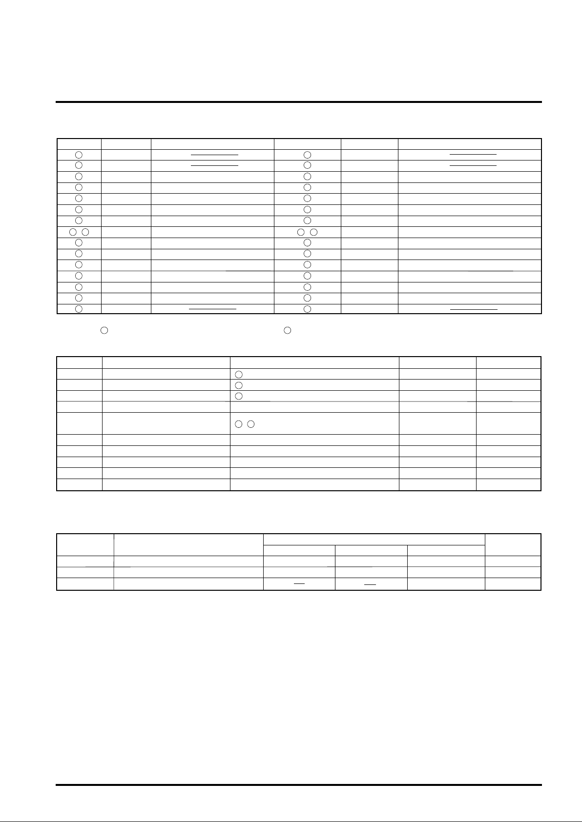
PIN DESCRIPTIONS
Pin No. Symbol Function
1 42
N.C
2
N.C
3
4
FGS FG pulse select
5
FG Frequency generator output
6
CI Phase Compensation
7
BRS Reverse torque mode select
GND
15
16
17
18
19
20
21
S
R
V
CC2 12V supply voltage
EC
ECR
V
CC1
HB
N.C
Start / Stop S/S
GND
Motor current sense
Motor speed control
The reference voltage for EC
5V supply voltage
Bias for Hall Sensor
* Pull-up resistors (10kohm) are included in the circuits connected to [FG] pin.
* Note1. The pin (TP) is test terminal. Please make an open the pin (TP).
ABSOLUTE MAXIMUM RATING (Ta=25˚C)
Symbol Rating Unit
R
S
CC2 12V supply voltage 16 V
V
VCC1
Motor supply voltage
5V supply voltage V
Io Output current 1.5 A
VH(c)
Pt
Kθ
Tj
Sensor amp.
Differential input range
Power dissipation
Thermal derating
Junction temperature
Topr Operating temperature -20 – +75
Tstg
Storage temperature
*Note2 ; The ICs must be operated within the Pt (power dissipation) or the area of safety operation
Parameter Conditions
15 pin
16 pin
19 pin
Note 2
23 – 28 pins
Free Air
Free Air
Pin No. Symbol Function
N.C
41
40
39
38
37
36
29 –358 –14
28
27
26
25
24
23
22
2424
N.C
W
V
U
MGND
TP
GND
Hw-
Hw+
HvHv+
HuHu+
N.C
Motor drive output W
Motor drive output V
Motor drive output U
Motor GND
Test
GND
Hw- Sensor amp. input
Hw+ Sensor amp. input
Hv- Sensor amp. input
Hv+ Sensor amp. input
Hu- Sensor amp. input
Hu+ Sensor amp. input
16 V
7.0
4.5
1.2
9.6
150
-40 – +125
Note1
V
W
mW/˚C
˚C
˚C
˚C
RECOMMENDED OPERATING CONDITIONS
Symbol Parameter
CC1
V
CC2 12V Power supply V13.24.5 12.0
V
5V Power supply
Io Output drive current
Min. Typ. Max.
Limits
5.04.5 5.5
1000
Unit
V
mA
Page 3
MITSUBISHI <CONTROL / DRIVER IC>
M56787FP
SPINDLE MOTOR DRIVER
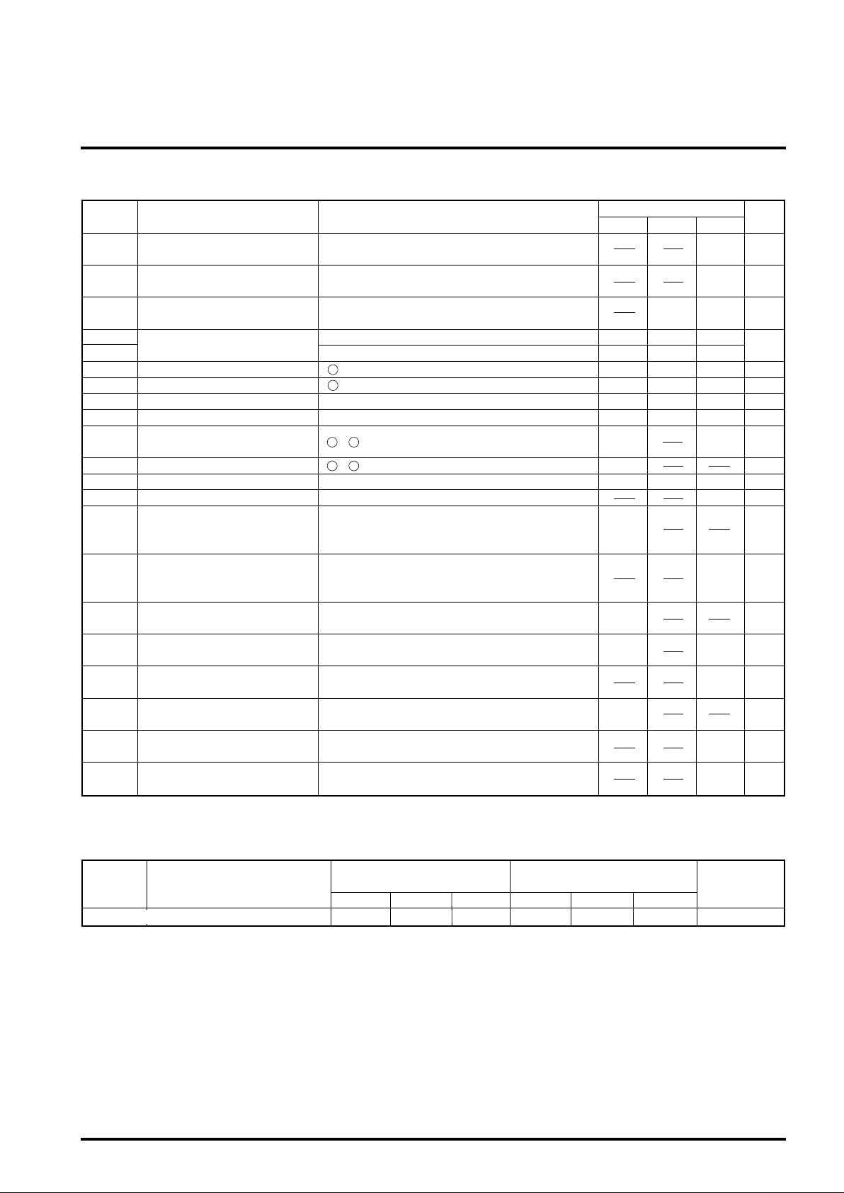
ELECTRICAL CHARACTERISTICS (VCC1=5V, VCC2=12V , Ta=25˚C unless otherwise noted.)
Symbol Parameter
Isleep Sleep Mode Supply current
Supply currentIcc
Vsat Saturation voltage
ECdead-
ECdead+
Control voltage dead zone
ECR Reference voltage Input range
EC Control voltage Input range
CC1& VCC2 pin total Current
V
(at S/S pin low or open)
CC1& VCC2 pin total Current
V
(EC=ECR=1.5V) [S/S pin High]
Top and Bottom saturation voltage.
(Load current :500mA)
EC < ECR
EC > ECR
18
pin [3.3V DSP available]
17
pin..[3.3V DSP available]
Conditions
Min. Typ. Max.
Gio Control gain Io = Gio / Rsense [A/V] 0.4 V/V0.460.34
Vlim Control limit Ilim = Vlim / Rsense [A] 0.3 0.330.27 V
VH com
VHmin Hall sensor amp. input signal level
Hall sensor amp
common mode input range
23 – 28
pins23 – 28
pins
VHb Hall bias terminal output voltage Load current (IHb) =10 mA.
IHb Hall bias terminal sink current
[S/S]pin input voltage when it starts up the motor.
Von
Motor start voltage
*The IC is in the active condition.
*The hall bias are available.
[S/S]pin input voltage when it stops the motor.
Voff
Motor stop voltage
*The IC is in the sleep condition.
*The hall bias are off.
V
iH1 3.6 VBRS input high voltage
ViM
BRS input middle voltage
BRS input voltage that the short braking is selected
when the reverse torque.
BRS input voltage that the free run is selected when
the reverse torque.
Note3.
BRS input voltage that the reverse braking is selected
when the reverse torque.
ViH2 2.0 VLogic input high voltage
V
VOL
iL2
Logic input
Low voltage
[FG] pin
output low voltage
[FGS] input voltage
when it is HIGH.
[FGS] input voltage
when it is LOW.
Io current = 1mA 0.5 V
Limits
10
10
1.2 1.9 V
-60 -30 0
+600 +30
0 3.3
1.65 V
1.650 3.3
1.3 4.4
2.0
0.8
0.8 VViL1 BRS input low voltage
0.8 V
Unit
µA
mA
mV
V
V
mVp-p60
V0.85 1.20.6
mA30
V
V
V2.21.6
*Note3. The ViM is the limit in case of external voltage input control. The free run mode is selected when the BRS pin is open, too.
THERMAL CHARACTERISTICS
Symbol Parameter Unit
TSD
Thermal Shut Down 165
Function start temperature of IC Function stop temperature of IC
Min. Typ. Max. Min. Typ. Max.
125
˚C
Page 4

The relationshipwith I/O control and the brakingmode
MITSUBISHI <CONTROL / DRIVER IC>
M56787FP
SPINDLE MOTOR DRIVER
BRS=LOW
Figure 1.
BRS=Hi
Current limit
0 – +60mV
0.8A/V
Forward Torque
REVERSE BRAKING
Reverse Torque
0.8A/V
0
0 – -60mV
Current limit
SHORT BRAKING
Reverse Torque
EC - ECR
The braking mode is selected flexibly by using the BRS
terminal.
The relationship between the EC-ECR (the difference
between (EC<control voltage> and ECR <reference
voltage> ) and the torque is shown in Figure 1,2 and 3.
The current gain is 0.8A/V (at sensing resistor :0.5ohm)
in forward torque directions, and the dead zone is from
0mV to 60mV.
When the reverse brake mode(BRS=Lo) is selected,
the coil current gain under the reverse torque control is
the same with in forward torque directions.
Figure 2.
BRS=Open
Figure 3.
0.8A/V
Forward Torque
0.8A/V
Forward Torque
0
0
0 – -60mV
Current limit
FREE RUN
0 – -60mV
Current limit
EC - ECR
EC - ECR
When the short brake mode(BRS=Hi) is selected, the
coil current under the reverse torque control depends on
the back emf. and the coil resistance.
When the free run mode(BRS=open) is selected,
the coil current under the reverse torque control
(EC-ECR>0) becomes zero and in free run
situation.
Page 5

THERMAL DERATI NG
MITSUBISHI <CONTROL / DRIVER IC>
M56787FP
SPINDLE MOTOR DRIVER
6.0
(W)
4.0W using H-type board
5.0
3.0W using I-type board
4.0
2.7W using J-type board
3.0
2.0
Power Dissipation (Pdp)
1.0
0 25 50 75 100 125 150
Ambient Temperature Ta (˚C)
HALL AMPLIFIER INPUT AND COMMUTATION
The relationship between the hall amplifier inputs voltage and the
motor current outputs is shown in Figure 4.
This IC's package is POWER-SSOP, so
improving the board on which the IC is mounted
enables a large power dissipation without a heat
sink.
For example, using an 1 layer glass epoxy resin
board, the IC's power dissipation is 2.7W at
least. And it comes to 4.0W by using an improved
2 layer board.
The information of the H, I, J type board is shown
in the board information.
Hall
inputs
Output
current
Figure 4.
Hw+
Hv+
U WV
Hu+
Hall elements
V
V
SOURSE
SINK
UVW WU
W
V
W
U
U
FORWARD
EC<ECR
U
Outer loator
W
V
U
W
V
REVERSE
EC>ECR
Page 6

SLEEP MODE FUNCTION
START / STOP (S/S pin)
LOW or OPEN HIGH
Motor Stop
Bias off
Hall-Bias off
Figure 5.
Motor on
Bias on
Hall-Bias on
FG FUNCTION
FG pulse select (FGS pin)
LOW or OPEN HIGH
NX1 pulse NX3 pulse
Figure 6.
MITSUBISHI <CONTROL / DRIVER IC>
M56787FP
SPINDLE MOTOR DRIVER
Figure 5 shows the sleep mode function. If the [S/S] pin is set to be open or low,
the motor drive outputs have high impedance and the motor stops. Then, the IC
bias current wil be a slight current (please refer to the electrical characteristics),
and the hall bias output will be cut off. When the [S/S] pin input is high, all the
circuits will work.
It is possible for user to switch the output pulse numeric by external
logic control using FG pulse select terminal [FGS].
Figure 6 shows the FG pulse select function.
The FG pin outputs the square pulse signal synchronizing with the hall
inputs [Hv+ and Hv-] timming when FGS=LOW or OPEN. When
FGS=HIGH, it outputs the square pulse signal of 3 times.
The FG pin is pulled-up to VCC1 by an internal resistor [typ. 10Kohm].
BRAKING MODE SELECT FUNCTION
Braking mode select [BRS] pin
HIGH SHORT BRAKE
OPEN
LOW
Figure 7.
FREE RUN
REVERSE BRAKE
It is possible to select three kinds of mode [the reverse braking,the short
braking and the free run] in reverse torque by logic control using the
BRS terminal.
Figure 7 shows the function table of the braking mode select.
It is the reverse braking when BRS is LOW,the short braking when BRS
is HIGH and the free run when BRS is OPEN.
Page 7

APPLICATION CIRCUIT
MITSUBISHI <CONTROL / DRIVER IC>
M56787FP
SPINDLE MOTOR DRIVER
104
10µF12V
Control
PWM1
Reference
PWM2
5V
10µF
0.5
V
CC2
EC
ECR
CC1
V
1
N.C
2
N.C
S/S
3
FGS
4
FG
5
C
I
6
BRS
7
8
9
10
11
12
13
14
15
R
S
16
17
18
19
20
HB
21
N.C N.C
CTL
BRAKING
MODE
CHANGE
LIMIT
BIAS..TSD
HALL
BIAS
FG
REVERSE
DETECT
SENSE
120° MATRIX
CURRENT
W
V
U
+-+- +-
N.C
N.C
MGND
TP
42
41
W
40
V
39
U
104
38
37
36
35
34
33
32
31
30
29
28
27
26
25
24
23
22
104
Please make an open
36
pin(TP) terminal.
Hw-
Hw
Hw+
Hv-
Hv
Hv+
Hu-
Hu
Hu+
104
Hall bias
resistor
Page 8

AREA OF SAFTY OPERATION
2.0
1.5
1.0
0.5
0.3
Corrector current IC [A]
MITSUBISHI <CONTROL / DRIVER IC>
M56787FP
SPINDLE MOTOR DRIVER
Tpw=500msec [Actual Data]
Tpw=4msec
0.1
Measurement circuits
1 pulse
Emitter current control
512 1034 67
Voltage during corrector and emitter
+
-
VCE [ volt ]
IC
Power supply
VCE
20 30 50
1612
IC
VCE
Tpw
measured
characteristics
 Loading...