

Page 1
MITSUBISHI <CONTROL / DRIVER IC>
)
(-)
)
(-)
)
(-)
)
(-)
)
M56759FP/AFP
4-CHANNEL ACTUATOR DRIVER
DESCRIPTION
The M56759 is a semiconductor integrated circuit designed for a
CD-ROM actuator driver. This device can function 4-channelactuators by 1 chip due to include 4 channel BTL drivers.
Three channels of this device, ch1, ch2 and ch3 can be controlled
by PWM pulse. Two of them, ch1 and ch2 can also act in the
Current Control mode.
Furthermore, this device includes two mute circuits and TSD
function.
FEATURES
● Low saturation voltage (at bootstrap).
●(typical 0.7V at load current 500mA)
●Wide supply voltage range.
(4.5V to 13.2V)
●Low cross-over distortion.
●Two naked Operational Amplifiers
●Divided Motor power supplies into three parts
APPLICATION
CD-ROM
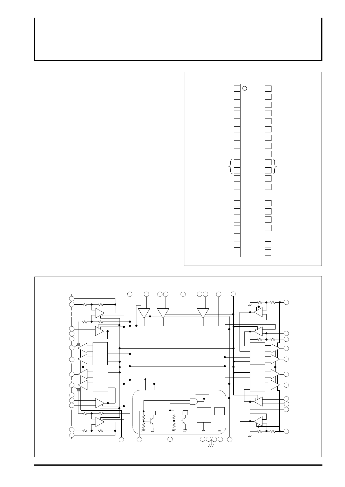
PIN CONFIGURATION(TOP VIEW
VCC2
VREF
VREF0
IN3IN3+
Vm3
OUT3
VM3
VM3(+
GND
VM4(+
VM4
IN4A-
Vm2
IN4B-
OP1OUT
OP1OP1+
OP2+
OP2-
1
2
3
4
7
8
13
14
15 28
16
17
18 25
19
20
21
Outline 42P2R-D
42
41
40
39
385
376
36
35
M56759FP/AFP
349
3310
3211
3112
30
29
27
26
24
23
22
MUTE2
MUTE1
SOUT2
SIN2IN2+
IN2OUT2
VM2
VM2(+
GND
VM1(+
VM1
OUT1
IN1IN1+
Vm1
SIN1SOUT1
VCC1
OP2OUT
BLOCK DIAGRAM
24
SOUT1
25
SIN1-
IN1+
27
28
IN1-
29
OUT1
31
VM1(+)
30
VM1(-)
35
VM2(-)
VM2(+)
34
36
OUT2
37
IN2-
38
IN2+
39
SIN2-
40
SOUT2
A4
+
OP1
OP1
OUT
17181920 21
TSD
VCC2
23
VCC1
1
15
Vm2
+
A1
-
+
E4
CH4
CH3
E3
A1
-
+
-
-
+
+
-
-
+
-
A3
+
-
A1
+
16
14
12
13
8
9
4
5
7
6
IN4BIN4A-
VM4(+)
VM4(-)
VM3(-)
VM3(+)
IN3IN3+
OUT3
Vm3
OP2
VREFVREF0
OP2+ OP2-
23 22
S1
-
A3
+
+
A3
-
E1
+
CH1
-
+
+
CH2
-
+
E2
-
A3
+
+
A3
-
S2
Vm1
-- -
+
A2 A4
BIAS
1ch
2ch
3ch
41
MUTE1
OUT
OP1+ OP1-
+
OP2
VCC2
VREF0
VCC1
Hi:Sleep
4ch
SLEEP
42 10 112632 33
MUTE2
GND (4PIN)
Page 2
j
,2,
g
g
y
y
PIN DESCRIPTIONS
(-)
)
(+)
)
(-)
)
(+)
)
mbol
S
1
VCC2
2
VREF
3
VREF0
4
IN3-
5
IN3+
6
Vm3
7
OUT3
8
VM3
9
VM3(+
10 11
to
12
13
14
15
16
17
18
19
20
21
GND
VM4
VM4(IN4AVm2
IN4BOP1OUT
OP1OP1+
OP2+
OP2-
Bootstrap power supply
Reference voltage input
Reference voltage output
E3 amplifier inverted input
E3 amplifier non-inverted input
Motor power supply-3
E3 amplifier output
CH3 inverted output
CH3 non-inverted output
GND
CH4 non-inverted output
CH4 inverted output
E4 amplifier low gain input
Motor power supply-2
E4 amplifier high gain input
OP1 amplifier output
OP1 amplifier inverted input
OP1 amplifier non-inverted input
OP2 amplifier non-inverted input
OP2 amplifier inverted input
MITSUBISHI <CONTROL / DRIVER IC>
Pin No. S
22
OP2OUT
23
VCC1
24
SOUT1
25
SIN1-
26
Vm1
IN1+
27
28
IN1OUT1
29
30
VM1
31
VM1(+
32 33
GND
to
VM2
34
35
VM2(-
36
OUT2
IN2-
37
38
IN2+
SIN2-
39
40
SOUT2
41
MUTE1
MUTE2
42
M56759FP/AFP
4-CHANNEL ACTUATOR DRIVER
mbolPin No. Function
OP2 amplifier output
5V power supply
S1 amplifier output
S1 amplifier inverted input
Motor power supply-1
E1 amplifier non-inverted input
E1 amplifier inverted input
E1 amplifier output
CH1 inverted output
CH1 non-inverted output
GND
CH2 non-inverted output
CH2 inverted output
E2 amplifier output
E2 amplifier inverted input
E2 amplifier non-inverted input
S2 amplifier inverted input
S2 amplifier output
CH1, 2 and 3 mute
CH4 mute
Function
ABSOLUTE MAXIMUM RATINGS (Ta=25˚C)
Symbol Rating
VCC2
Vm
VCC1
Io
Vin1
Vin2
Pt
Kθ
T
Topr
Tstg
Bootstrap power supply
Motor power supply
5V power supply
Output Current
Maximum input voltage of terminals
Power dissipation
Thermal deratin
Junction temperature
Operatin
Storage temperature
Parameter Conditions
1
pins input voltage
26 15
, and pins input voltage
23
pin input voltage
2 4 5 14 16 18 19 20 21 27 28 37 38 41 42
, , , , , , , , , , , , , , pins
25 39
, pins
6
Free Air
Free Air
temperature
0 – VCC1
0 – Vm1
-20 – +70
-40 – +150
RECOMMENDED OPERATING CONDITIONS
Symbol UnitParameter
VCC1 5.04.5
VCC2
Vm1
5V power supply
Bootstrap power supply
3
Motor power supply-1, 2, 3
Min.
Limits
Typ.
Vm+1.0
5.0
Max.
5.5
V
V
V
15
15
7.0
700
1.2
9.6
150
Unit
V
V
V
mA
V
W
mW/˚C
˚C
˚C
˚C
Page 3
MITSUBISHI <CONTROL / DRIVER IC>
y
µ
µ
µ
µ
)
M56759FP/AFP
4-CHANNEL ACTUATOR DRIVER
ELECTRICAL CHARACTERISTICS
mbol Conditions UnitParameter
S
ICC1
ICC2
ICC3
VsatCH1
VsatCH2
VsatCH3
VsatCH4
Vmute-on
Vmute-off
Imute
VinOP
VoutOP
VofOP Vin=2.5V (at buffer)
IinOP
IofOP
GBOP
VinE
VoutE
VofE
IinE
IofE
VoutS
VinVREF
VofVREF
VofCH1
VofCH2
VofCH3
VofCH4
VofS1 S1 output offset voltage
VofS2
GainCH1
GainCH2
GainCH3
GainCH4
GainS1
GainS2
Supply current-1
Supply current-2
Sleep Mode Supply current-3
Ch1 Saturation voltage
Ch2 Saturation voltage
Ch3 Saturation voltage
Ch4 Saturation voltage
Mute-on voltage
Mute-off voltage
Mute terminals input current
OP1and OP2
OP1and OP2
OP1and OP2
OP1and OP2
OP1and OP2
OP1and OP2
E1,E2 and E3
E1,E2 and E3
E1,E2 and E3
E1,E2 and E3
E1,E2 and E3
S1 and S2 amplifier output voltage range
VREF buffer amplifier Input voltage range
VREF buffer amplifier offset voltage
Ch1 output offset voltage
Ch2 output offset voltage
Ch3 output offset voltage
Ch4 output offset voltage
S2 output offset voltage
Ch1 power amplifier voltage gain
Ch2 power amplifier voltage gain
Ch3 power amplifier voltage gain
Ch4 power amplifier voltage gain
S1 amplifier voltage gain
S2 amplifier voltage gain
amplifier Input voltage range
amplifier output voltage range
amplifier input offset voltage
amplifier input current
amplifier input current offset
amplifier GB
amplifier Input voltage range
amplifier output voltage range
amplifier input offset voltage
amplifier input current
amplifier input current offset
unless otherwise noted
1 26 15 6
, , , pins supply current (Vref=Vctl=2.5V)
23
pins[VCC1] supply current (Vref=Vctl=2.5V)
1 23 26 15 6
, , , , pins supply current (MUTE1,2=H)
Top and Bottom saturation voltage.
Load current 500mA. At bootstrap.
Mute-on
Mute-off
41 42
and pin input current at 5V input voltage.
Io=±2.0mA
inverted input = non-inverted input = 2.5V
inverted input = non-inverted input = 2.5V
No load
Vin=2.5V (at buffer)
inverted input = non-inverted input = 2.5V
inverted input = non-inverted input = 2.5V
No load
2
pin input voltage = 2.5V
when the OUT1 voltage is adjusted at the same
VREFO voltage, at VREF=2.5V
when the OUT2 voltage is adjusted at the same
VREFO voltage, at VREF=2.5V
when the OUT3 voltage is adjusted at the same
VREFO voltage, at VREF=2.5V
when the IN4- voltage is adjusted at the same
VREFO voltage, at VREF=2.5V
SOUT1-VREFO (at SI N1[-] = VM1[+] )
at VREF=2.5V
SOUT2-VREFO (at SI N2[-] = VM2[+] )
at VREF=2.5V
{VM1(+)–VM1(-)}
(OUT1–VREFO)
{VM2(+)–VM2(-)}
(OUT2–VREFO)
{VM3(+)–VM3(-)}
(OUT3–VREFO)
-1 · {VM4(+)–VM4(-)}
(I N4A[-]–VREFO)
{SOUT1 - VREFO}
(VM1[+] - SI N1[-] )
{SOUT2 - VREFO}
(VM2[+] - SI N2[-] )
(Ta=25˚C, VCC1=Vm1=Vm2=Vm3=5V, VCC2=12V, no-load current
at VREF=2.5V
at VREF=2.5V
at VREF=2.5V
at VREF=2.5V
at VREF=2.5V
at VREF=2.5V
Limits
Min. Typ. Max.
24 36 mA
9.5 15 mA
500
0.8 1.20 V
0.8 1.20 V
0.5 0.9 V
0.6 1.0 V
2.0
0.8 V
170 250
0.5
0.5
-10
-1.0
-100
2.3
0.5
1.0
-10
-1.0
-100
1.0
1.5
-10
-26
-26
-26
-26
-20
-20
13.1
13.1
19.1
3.17
5.11
5.11
VCC2-1.0
VCC1-0.5
+10 mV
-0.15 0
0 +100 nA
4 MHz
VCC2-2.0
VCC1-0.5
+10 mV
-0.15 0
0 +100 nA
VCC1-0.5
2.5
VCC1-1.2
+10 mV
+26 mV
+26 mV
+26 mV
+26 mV
+20 mV
+20 mV
14 14.8 dB
14 14.8 dB
20 20.8 dB
4.08 4.91 dB
6.02 6.85 dB
6.02 6.85 dB
A
V
A
V
V
A
V
V
A
V
V
Page 4
(
)
INPUT and OUTPUT CHARACTERISTICS of EACH CHANNELS
(
)
(
)
(
)
(
)
MITSUBISHI <CONTROL / DRIVER IC>
M56759FP/AFP
4-CHANNEL ACTUATOR DRIVER
CH1 amplifier
2.5V
CH2 amplifier
2.5V
VREF
2
VREF0
3
27
IN1+
28
IN1-
29
OUT1
GainCH1
VREF
2
VREF0
3
38
IN2+
37
IN2-
36
OUT2
GainCH2
Output of non-inverted Amp.
Gain = X2.5
+
-
E1
+
-
Differential voltage gain = X5
+
-
E2
+
-
Differential voltage gain = X5
CH1
Output of inverted Amp.
(Gain = X-2.5)
Output of non-inverted Amp.
Gain = X2.5
CH2
Output of inverted Amp.
(Gain = X-2.5)
<INPUT>
OUT1
+
31
-
+
-
VM1+
30
VM1-
VREFO
<OUTPUT>
VREFO
0.5V
0.2V
0.5V
VM1+
VM1-
<INPUT>
OUT2
+
34
-
+
-
VM2+
35
VM2-
VREFO
<OUTPUT>
VREFO
0.5V
0.2V
0.5V
VM2+
VM2-
CH3 amplifier
Output of non-inverted Amp.
Gain = X5
VREF
2
VREF0
3
5
IN3+
2.5V
4
IN3-
7
OUT3
GainCH3
+
-
CH3
E3
+
-
Output of inverted Amp.
Gain = X-5
Differential voltage gain = X10
+
-
+
-
9
8
VM3+
VM3-
<INPUT>
VREFO
<OUTPUT>
Vrefm3
Vm3/2
1.0V
0.2V
1.0V
OUT3
VM3+
VM3-
Page 5

MITSUBISHI <CONTROL / DRIVER IC>
(
)
(
)
M56759FP/AFP
4-CHANNEL ACTUATOR DRIVER
CH4 amplifier
2.5V
Vctl4
S1 amplifier
IN4BIN4A-
SIN1-
25
VM1+
31
VREF
2
VREF0
3
16
14
GainCH4
E4
25K 4K
(Gain = X-0.16)
5K 10K
+
5K 10K
GainS1
Output of non-inverted Amp.
Gain = X5
+
-
CH4
+
-
Output of inverted Amp.
(Gain = X-5)
Differential voltage gain = X1.6
24
3
Voltage gain = X2
SOUT1
VREFO
+
-
+
-
<INPUT>
12
VM4+
13
VM4-
VREFO
<OUTPUT>
Vrefm4
Vm4/2
1.0V
0.8V
0.8V
VM4-
Vctl4
VM4+
<INPUT>
SIN1-
VM1+
<OUTPUT>
VREFO
0.5V
SOUT1
1.0V
S2 amplifier
SIN2-
39
VM2+
34
5K 10K
+
5K 10K
GainS2
Voltage gain = X2
40
3
SOUT2
VREFO
<INPUT>
VM2+
<OUTPUT>
VREFO
SIN2-
0.5V
SOUT2
1.0V
Page 6

MITSUBISHI <CONTROL / DRIVER IC>
)
,
,
)
)
)
M56759FP/AFP
4-CHANNEL ACTUATOR DRIVER
<BASICALLY CHARACTERISTICS> This data is an example for typical sample.
Output saturation voltage and Load current characteristic.
BOOTSTRAP
CH1
5.0
Vm1=VCC1=5V
VCC2=12V
CH2
5.0
Vm1=VCC1=5V,VCC2=12V
4.0
0.3V
VM1+,VM1-
3.0
2.0
Output Voltage (V)
1.0
0.5V
0
0.2 0.4 0.5
0.35V
0.6 0.8 1.0
VM1+
VM1-
Load Current (mA
CH3
5.0
4.0
0.22V
Vm3=VCC1=5V
VM3+,VM3-
VCC2=12V
0.46V
CH4
3.0
2.0
Output Voltage (V)
1.0
0.24V
0
0.2 0.4 0.5 0.6 0.8 1.0
VM3+,VM3-
0.5V
Load Current (mA) Load Current (mA
NON-BOOTSTRAP
CH1 CH2
5.0
Vm1=VCC1=VCC2=5V Vm1=VCC1=VCC2=5V
Output Voltage (V)
Output Voltage (V)
4.0
3.0
2.0
1.0
5.0
4.0
3.0
2.0
1.0
5.0
0.3V
0.5V
0
0.2 0.4 0.5 0.6 0.8 1.0
VM2+,VM2-
0.3V
VM2+
VM2-
Load Current (mA
Vm2=VCC1=5V,VCC2=12V
0.3V
0.3V
0
0.2 0.4 0.5 0.6 0.8 1.0
VM4+,VM4-
0.6V
0.6V
VM4+,VM4-
CH3
Output Voltage (V)
Output Voltage (V)
4.0
3.0
2.0
1.0
5.0
4.0
3.0
2.0
1.0
1.0V
VM1+,VM1-
4.0
3.0
1.0V
VM2+,VM2-
2.0
0.5V
0
0.2 0.4 0.5 0.6 0.8 1.0
0.35V
VM1+
VM1-
Output Voltage (V)
1.0
0
0.5V
0.3V
0.2 0.4 0.5 0.6 0.8 1.0
VM2+
VM2-
Load Current (mA) Load Current (mA)
Vm3=VCC1=VCC2=5V
VM4+,VM4-
CH4
5.0
Vm2=VCC1=VCC2=5V
VM4+,VM4-
4.0
1.0V
3.0
2.0
0.24V
0
0.2 0.4 0.5 0.6 0.8 1.0
VM3+,VM3-
0.5V
Output Voltage (V)
1.0
0
Load Current (mA
1.0V
0.6V
0.3V
VM4+,VM4-
0.2 0.4 0.5 0.6 0.8 1.0
Load Current (mA)
Page 7

THERMAL DERATING
0
03.0
0
0
2
0
5
(˚C)
6.
(W)
5.
4.
4.
2.
1.
Power dissipation (Pdp)
1.
MITSUBISHI <CONTROL / DRIVER IC>
M56759FP/AFP
4-CHANNEL ACTUATOR DRIVER
With infinite heatsink
Without heatsink
02550
Ambient temperature (Ta)
75
100 125 150
Page 8

MITSUBISHI <CONTROL / DRIVER IC>
M56759FP/AFP
4-CHANNEL ACTUATOR DRIVER
APPLICATION CIRCUIT No.1
VCTL1
R1
R2
FOCUS
5V
TRACKING
VREFO
VCTL2
cf. R1=10K,R2=14K
Voltage gain = GainCH1
•
= 5 14 / 10
= 7 (V/V) =16.9dB
if. Ra=10
Current gain = 7/10 = 0.7 (A/V)
•
R2 / R1
MUTE2
42
MUTE1
41
24
25
SIN1-SOUT1
VREFO
IN1+
27
28
OUT1
29
VM1+ VM1-
31
Ra
30
26
23
VM2-
35
VM2+
34
OUT2
36
37
IN2+
38
SIN2-
39
40
19
18
17
•single input (linear signal)
•Direct voltage control
ch4
ch1, ch2,
ch3
10K
5K
+-
5K
IN1-
10K
10K
10K
+ -
+ -
12.5K 5K
-
+
Vm1
VCC1
GND
+ -
12.5K 5K
10K
10K
+-
IN2-
SOUT2
5K
5K
OP1+
OP1-
-
+
10K
+ -
10K
+ -
5K
12.5K
5K
12.5K
5K
5K
OP1OUT
2.5K
TSD
OP2OUT
4K
2.5K
2.5K
10K
+ -
+
-
+
12.5K
12.5K
-
+
12.5K2.5K
12.5K2.5K
+
-
12.5K2.5K
12.5K2.5K
+
-
12.5K2.5K
+
-
+
+ -
-
12.5K
-
10K10K
10K
25K
VREF0
3
VREF
2
Vm2
15
IN4B-
16
14
IN4A- VM4+ VM4-
12
13
VCC2
1
8
VM3- VM3+ Vm3
9
OUT3
7
IN3-
4
5
IN3+
6
OP2+
20
OP2-
21
22
2.5V
5V
TRAY
M
12V
TRAVERSE
M
VREFO
5V
VCTL4
VCTL3
Page 9

MITSUBISHI <CONTROL / DRIVER IC>
M56759FP/AFP
4-CHANNEL ACTUATOR DRIVER
APPLICATION CIRCUIT No.2
VCTL1
R1
R2
*Phase compensation filter
Rs
FOCUS
5V
TRACKING
VCTL2
VREFO
42
41
24
25
SIN1-
VREFO
IN1+ IN2+
27
28
OUT1
29
31
VM1+ VM1-
Ra
30
26
23
VM2-
35
34
OUT2
36
37
38
SIN2-
39
40
19
18
17
•single input (linear signal)
•Direct current control (for FOCUS and TRACKING)
ch4
MUTE2
ch1, ch2,
ch3
MUTE1
SOUT1
5K
5K
IN1-
10K
10K
10K
S1
+-
10K
+ -
E1
5K
+ -
12.5K 5K
-
+
+ -
+-
-
+
10K
+ -
10K
+ -
12.5K
5K
12.5K
5K
5K
OP1OUT
GND
VM2+
IN2-
SOUT2
5K
Vm1
VCC1
10K
10K
5K
OP1+
OP1-
12.5K 5K
TSD
OP2OUT
2.5K
2.5K
2.5K
4K
10K
+ -
-
+
12.5K
12.5K
-
+
12.5K2.5K
12.5K2.5K
+
-
12.5K2.5K
12.5K2.5K
+
-
12.5K2.5K
+ -
+
-
12.5K
-
+
-
+
10K
10K10K
25K
VREF0
VREF
Vm2
15
IN4B-
16
14
IN4A-
VM4+ VM4-
12
13
VCC2
VM3- VM3+ Vm3
OUT3
IN3-
IN3+
OP2+
20
OP2-
21
22
3
2.5V
2
5V
TRAY
M
12V
1
TRAVERSE
8
M
9
7
VREFO
4
5
6
5V
VCTL4
VCTL3
cf. R1=10K,R2=14K,Rs=1
Current gain = R2 / [R1 · GainS1 · Rs]
= 14 / [10 · 2 · 1]
= 0.7 (A/V)
Page 10

MITSUBISHI <CONTROL / DRIVER IC>
M56759FP/AFP
4-CHANNEL ACTUATOR DRIVER
APPLICATION CIRCUIT No.3
MUTE2
42
MUTE1
41
PWM2
PWM1
24
5K
25
C1
C2
R1
R1
R2
VREFO
FOCUS TRACKING
VREFO
R4
R3
R3
PWM2
R2
C1
5V
C2
R4
PWM1
27
28
29
31
30
26
23
35
34
36
37
38
39
40
19
18
17
SIN1-SOUT1
IN1+ IN2+
IN1-
OUT1
VM1+ VM1-
10K
10K
GND
VM2-
VM2+
OUT2
IN2-
SIN2-
SOUT2
5K
5K
Vm1
VCC1
10K
10K
5K
OP1+
OP1-
•Differential PWM input (for FOCUS, TRACKING and TRAVERSE)
•Direct voltage control
ch4
ch1, ch2,
ch3
10K
10K
4K
+ -
-
+
12.5K
12.5K
-
+
12.5K2.5K
12.5K2.5K
+
-
12.5K2.5K
12.5K2.5K
+
-
12.5K2.5K
+ -
+
-
12.5K
-
+
-
+
10K10K
10K
+-
10K
+ -
5K
+ -
12.5K 5K
-
+
12.5K
5K
12.5K
+ -
5K
12.5K 5K
+-
5K
-
+
10K
+ -
10K
+ -
OP1OUT
2.5K
2.5K
2.5K
TSD
OP2OUT
25K
VREF0
VREF
Vm2
15
IN4B-
16
14
IN4A- VM4+ VM4-
12
13
VCC2
VM3- VM3+ Vm3
OUT3
IN3-
IN3+
OP2+
20
OP2-
21
22
3
2.5V
2
5V
VCTL4
TRAY
M
12V
1
TRAVERSE
8
M
9
C3
7
R6
4
5
R5
6
5V
R6
R5
PWM1
VREFO
C3
PWM2
Page 11

MITSUBISHI <CONTROL / DRIVER IC>
M56759FP/AFP
4-CHANNEL ACTUATOR DRIVER
APPLICATION CIRCUIT No.4
PWM1
PWM2
MUTE2
42
MUTE1
VREFO
5V
41
24
25
27
28
29
31
30
26
23
35
34
36
37
38
39
40
19
18
17
SOUT1
SIN1-
IN1+ IN2+
OUT1
VM1+ VM1-
VM2-
OUT2
SIN2-
R1
R3
R3
PWM1
PWM2
R1
R2
C1
R2
C1
FOCUS TRACKING
C2
VREFO
R4
C2
R4
5K
IN1-
GND
VM2+
IN2-
SOUT2
5K
5K
10K
10K
10K
10K
5K
OP1+
OP1-
•Differential PWM input (for FOCUS, TRACKING and TRAVERSE)
•Direct current control (for FOCUS and TRACKING)
ch4
ch3
10K
+-
10K
+ -
+ -
12.5K 5K
+-
Vm1
VCC1
+ -
12.5K 5K
PA
+-
-
+
10K
+ -
10K
+ -
ch1, ch2,
5K
12.5K
5K
12.5K
5K
5K
OP1OUT
OP1
TSD
OP2OUT
2.5K
2.5K
2.5K
4K
10K
+ -
+
-
+
12.5K
12.5K
-
+
12.5K2.5K
12.5K2.5K
+
-
12.5K2.5K
12.5K2.5K
+
-
12.5K2.5K
+
-
+
+ -
10K
-
25K
12.5K
-
10K10K
VREF0
3
VREF
2
Vm2
15
IN4B-
16
14
IN4A- VM4+ VM4-
12
13
VCC2
1
8
VM3- VM3+ Vm3
9
OUT3
7
IN3-
4
5
IN3+
6
OP2+
20
OP2-
21
22
2.5V
5V
TRAY
M
12V
TRAVERSE
M
C3
R6
5V
VCTL4
R5
PWM1
VREFO
R6
R5
PWM2
C3
 Loading...