

Page 1
MITSUBISHI <CONTROL / DRIVER IC>
)
)
)
(+)
)
(-)
)
)
(+)
)
)
)
(-)
)
(+)
)
)
)
M56749FP
4 CHANNEL ACTUATOR MOTOR DRIVER
DESCRIPTION
The M56749FP is a semiconductor integrated circuit designed for a
CD-ROM actuator driver.
This device can function 4 channel actuators by 1 chip due to
include 4 channel BTL drivers.
Also, this device include a mute circuit, a Vcc check circuit and
TSD function.
FEATURES
●Lower saturation voltage.
(typical 1.35V at load current 500mA)
●Wide supply voltage range.
(4.5V to 13.2V)
●Lower cross-over distortion.
APPLICATION
CD-ROM
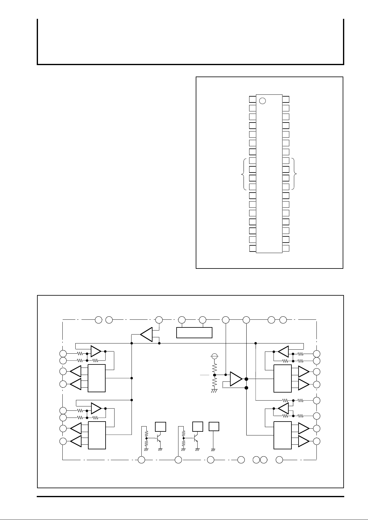
PIN CONFIGURATION(TOP VIEW
Vrefm-out
Mute3chMute4ch-
Vctl1L
Vctl1H
VM1(-
VM1(+
GND
VM2(+)
VM2(-)
Vctl2H
Vctl2L
Vm1
Vbs1
Vcc
1
2
3
4
7
8
10
13
14
15 22
16 21
17
18
36
35
34
33
325
316
30
M56749FP
29
289
27
2611
2512
24
23
20
19
Vref
Vrefm
SS . GND
Vctl4L
Vctl4H
VM4
VM4(+
GND
VM3
VM3(Vctl3(-)
Vctl3(+)
Vm2
Vbs2
-Por
BLOCK DIAGRAM
Vctl1L
4
Vctl1H
5
VM1
VM1(-
Vctl2L
Vctl2H
VM2(+
VM2(-
+
7
-
-
6
+
15
14
+
12
-
-
13
+
Vm1 Vbs1
+
-
CH1
+
-
CH2
Vref Vrefm
36 18 19 35 1 20 2116 17
+
-
Mute on : Low or open
3ch
Vcc -Por
- POR
Vm2
4ch
Vm2
2
TSD
Vrefm-out
+
-
Outline 36P2R-D
Vm2
Vbs2
CH4
CH3
+
-
+
-
-
+
+
-
+
-
+
33
32
30
31
22
23
25
24
Vctl4L
Vctl4H
VM4
VM4(-
Vctl3(+
Vctl3(-
VM3(+
VM3
8 11 26 293432
–
Mute3ch-
Mute4ch-
SS.GND
PGND (8PIN
–
Page 2
)
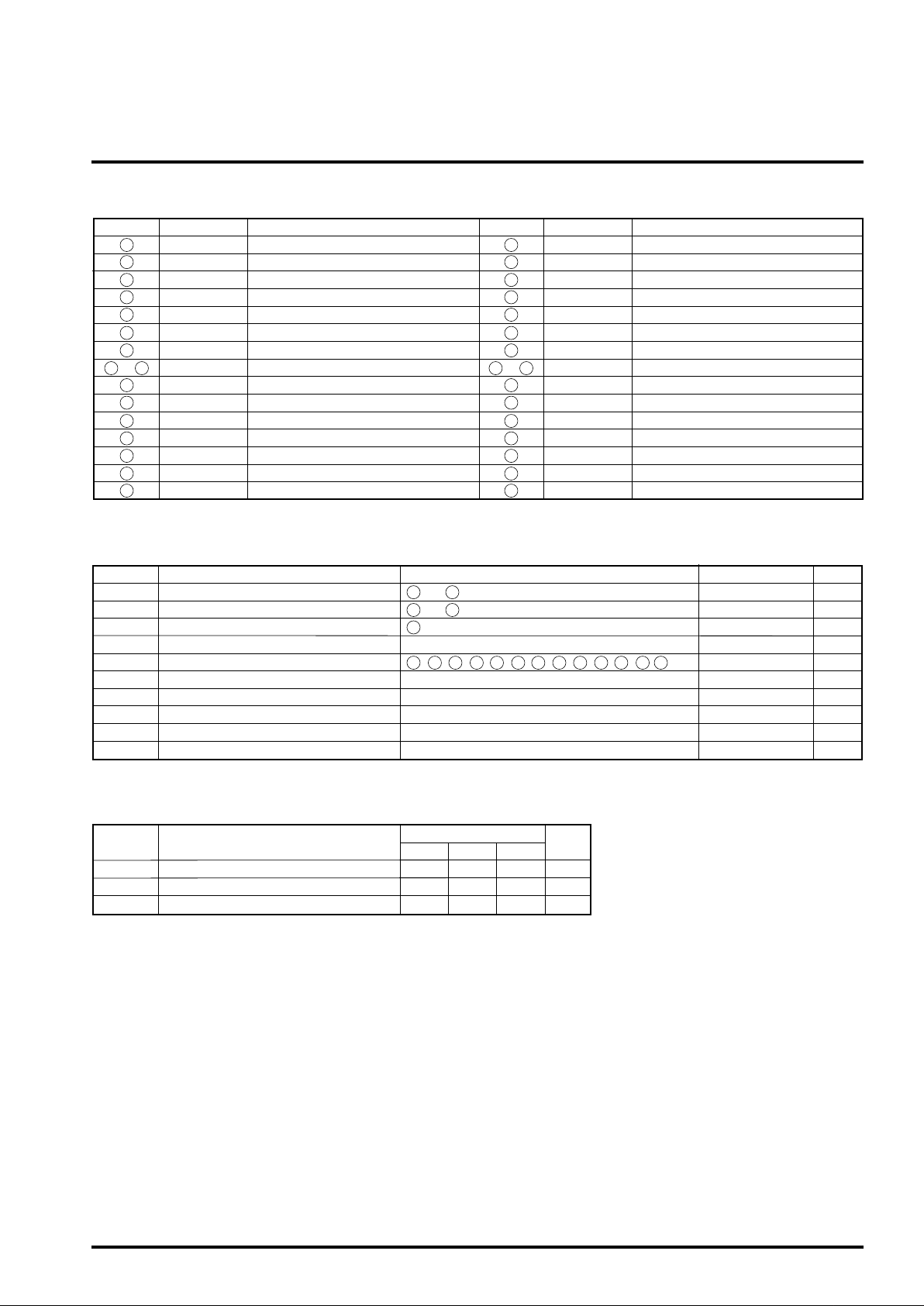
PIN DESCRIPTION
Pin No. Function
1
2
3
4
5
6
7
8 11
to
12
13
14
15
16
17
18
Symbol
Vrefm-out
Mute3chMute4chVctl1L
Vctl1H
VM1(-)
VM1(+)
GND
VM2(+)
VM2(-)
Vctl2H
Vctl2L
Vm1
Vbs1
Vcc
Vm2 middle voltage output
3th channel mute terminal
4th channel mute terminal
1st channel Low gain input
1st channel High gain input
1st channel inverted amp. output
1st channel non-inverted amp. output
GND
2nd channel non-inverted amp. output
2nd channel inverted amp. output
2nd channel High gain input
2nd channel Low gain input
Motor power supply-1
Bootstrap power supply-1
5V power supply
MITSUBISHI <CONTROL / DRIVER IC>
4 CHANNEL ACTUATOR MOTOR DRIVER
Pin No. Symbol
19
-Por
20
Vbs2
21
Vm2
22
Vctl3(+)
23
Vctl3(-)
VM3(-)
24
25
VM3(+)
26 29
GND
to
30
VM4(+)
31
VM4(-)
Vctl4H
32
Vctl4L
33
34
SS. GND
35
Vrefm
36
Vref Reference voltage input
M56749FP
Function
Vcc check signal output
Bootstrap power supply-2
Motor power supply-2
3th channel non-inverted amp. input
3th channel inverted amp. input
3th channel inverted amp. output
3th channel non-inverted amp. output
GND
4th channel non-inverted amp. output
4th channel inverted amp. output
4th channel High gain input
4th channel Low gain input
Small signal GND
Vm2 middle voltage monitor
ABSOLUTE MAXIMUM RATINGS(Ta=25˚C
Symbol Rating
Vbs
Vm
Vcc
Io
Vin
Pt
Kθ
Tj
Topr
Tstg
Bootstrap power supply
Motor power supply
5V power supply
Output Current
Maximum input voltage of terminals
Power dissipation
Thermal derating
Junction temperature
Operating temperature
Storage temperature
Parameter Conditions
17 20
and pins input voltage
16 21
and pins input voltage
18
pin input voltage
2 3 4 5 14 15 19 22 23 32 33 35 36
, , , , , , , , , , , , pins
Free Air
Free Air
0 – Vcc
-20 – +70
-40 – +150
RECOMMENDED OPERATING CONDITIONS
Symbol
Vcc V5.04.5
Vm1,Vm2
Vbs1,Vbs2
5V power supply
Motor power supply
Bootstrap power supply
Min.
Limits
Typ.
5.0
Vm+1.0
Max.
5.5
UnitParameter
V
V
15
15
7.0
700
1.2
9.6
150
Unit
V
V
V
mA
V
W
mW/˚C
˚C
˚C
˚C
Page 3

MITSUBISHI <CONTROL / DRIVER IC>
)
M56749FP
4 CHANNEL ACTUATOR MOTOR DRIVER
ELECTRICAL CHARACTERISTICS(Ta=25˚C, Vcc=Vbs1=Vbs2=Vm1=Vm2=5V, no-load current unless otherwise noted.
Symbol Parameter
Icc1
Icc2
Vsat
Vofs1
Vofs2
VPor
∆VPor
Vmute-on
Vmute-off
Imute
VrefmL
VrefmH
Vrefin
Sleep Mode Supply current-1
Sleep Mode Supply current-2
Saturation voltage
Output offset voltage-1
Output offset voltage-2
Vcc check voltage ( pin L to H)
Vcc check circuit Hysteresis
Mute-on voltage
Mute-off voltage
Mute terminals input current
Vref amp. Low output voltage
Vref amp. High output voltage
Vref amp. Input voltage range
Conditions
, , , pins input current (Vref=Vctl=2.1V)
16 17 20 21
18
pin input current (Vref=Vctl=2.1V)
Top and Bottom saturation voltage.
Load current 500mA.
1st, 2nd channel. Vref=Vctl=2.1V, Vm1=5V
3th, 4th channel. Vref=Vctl=2.1V,Vm2=Vbs2=12V
19
Vcc voltage when pin (-POR circuit)
returns to High from Low condition.
19
3th and 4th channels Mute-on.
3th and 4th channels Mute-off.
2 3
and pin input current at 5V input voltage.
1
pin output voltage at load current 1.0mA when Vrefm
35
( pin) inputs 0V.
1
pin output voltage at load current 0.5mA when Vrefm
35
( pin) inputs 5V.
36
pin input voltage range.
Vbs2-
Limits
Min. Typ. Max.
30
6.0
1.90
+26
+100
4.40
-26
-100
4.10
80
20
3.0
1.35
4.25
130 180
0.8
2.0
170 250
0.15
0.3
Vbs2-
2.25
1.5
1.9
2.1
Vcc-1.2
Unit
mA
mA
V
mV
mV
V
mV
V
V
µA
V
V
V
Voltagegain of each channel
Symbol Conditions UnitParameter
Gain1L
Gain1H
Gain2L
Gain2H
Gain3
Gain4L
Gain4H
1st channel voltage gain (L)
1st channel voltage gain (H)
2nd channel voltage gain (L)
2nd channel voltage gain (H)
3th channel voltage gain
4th channel voltage gain (L)
4th channel voltage gain (H)
{VM1(+)–VM1(-)}
(Vctl1L–Vref)
{VM1(+)–VM1(-)}
(Vctl1H–Vref)
{VM2(+)–VM2(-)}
(Vctl2L–Vref)
{VM2(+)–VM2(-)}
(Vctl2H–Vref)
{VM3(+)–VM3(-)}
Vctl3(+)–Vctl3(-)
{VM4(+)–VM4(-)}
(Vctl4L–Vref)
{VM4(+)–VM4(-)}
(Vctl4H–Vref)
(Vctl1L= pin)
(Vctl1H= pin)
(Vctl2L= pin)
(Vctl2H= pin)
(Vctl3(+)= pin)
(Vctl3(-)= pin)
(Vctl4L= pin)
(Vctl4H= pin is
4
5
15
14
22
23
33
32
connected 10kΩ)
Limits
Min. Typ. Max.
8.86 9.77 10.6 db
14.6 15.6 16.4 db
11.1 12.0 12.9 db
14.5 15.4 16.2 db
-3.07 1.94 -1.33 db
11.1 12.0 12.9 db
14.4 15.3 16.1 db
Page 4

)
(
)
(
)
Input and output characteristics of each channels
(
)
(
)
(
)
(
)
(
)
(
)
)
(
)
(
)
<Channel 1 Amp.>
Output of non-inverted Amp.
(Gain = X2.0)
10K
+
Reference
voltage
+
-
7.5K5K
Vref=2.1V
Output of inverted Amp.
(Gain = X2.0)
+
-
+
-
7
6
VM1+
VM1-
Vref
36
Vctl1L
4
Vctl1H
5
(Unit of resistance: Ω)
MITSUBISHI <CONTROL / DRIVER IC>
M56749FP
4 CHANNEL ACTUATOR MOTOR DRIVER
The voltage between the input and output
when a voltage is inputted from Vctl( pin).
<INPUT>
Vctl1L
Vref
2.1V
Vref
2.1V
1V
VM1-
<OUTPUT>
1.5V
1.5V
VM1+
4
<Channel 2 Amp.>
Vref
36
Vctl2L
15
Vctl2H
14
<Channel 3 Amp.>
36
Vref
Vctl3+
22
23
Vctl3-
7.5K
10K
10K
The voltage between the input and output
non-inverted Amp.
(Gain = X2)
+
Reference
voltage
+
-
7.5K5K
Vref=2.1V
inverted Amp.
(Gain = X2)
+
-
+
-
VM2+
12
13
VM2-
when a voltage is inputted from Vctl2( pin).
Vctl2L
Vref
2.1V
Vref
2.1V
1V
VM2-
VM2+
2.0V
2.0V
15
The voltage difference of 1V is inputted
non-inverted Amp.
(Gain = X2)
+
-
2K
+
-
2K
Reference
voltage
(Vrefm=
Vm2/2
inverted Amp.
(Gain = X2)
+
-
+
-
VM3+
25
VM3-
24
between Vctl3- and Vctl3+.
Vctl3-
Vref
2.1V
Vctl3+
VM3- VM3+
Vrefm
Vm2/2
1V
0.8V
<Channel 4 Amp.>
non-inverted Amp.
(Gain = X5)
18K
+
-
+
-
7.2K2K
Reference
voltage
(Vrefm=
Vm2/2
inverted Amp.
(Gain = X5)
+
-
+
-
VM4+
30
VM4-
31
Vref
36
Vctl4L
33
10kΩ
Vin4
32
Vctl4H
Vctl4H ( pin) is connected 10kΩ and the voltage
between a input (Vin4) and out when a voltage is
inputted from Vin4.
Vref
2.1V
Vrefm
Vm2/2
Vin4
VM4-
32
1V
VM4+
3.0V
3.0V
Page 5

BASICALLY CHARACTERISTICS (Typical value)
Output saturation voltage and Load current characteristic (Vbs=Vm=Vcc=5V)
5.0
(V)
0.84
0.89
0.95
4.0
3.0
Output voltage
2.0
1.0
0.06
0.12
0.18 0.24
100 200 300 400 500(mA)
Load current
FREQUENCY CHARACTERISTIC
MITSUBISHI <CONTROL / DRIVER IC>
M56749FP
4 CHANNEL ACTUATOR MOTOR DRIVER
Top side saturation voltage
1.00
This device can use this voltage value
for actuator drive.
Bottom side saturation voltage
1.05
0.30
40
(dB)
20
GAIN
0
-20
-40
0.03 0.06 0.1 0.3 0.6 1 3 6 10 30 60 100 300 600
THERMAL DERATING
6.0
5.0
4.5
4.0
3.0
GAIN
PHASE
Frequency
With infinite heatsink
Without heatsink
(kHZ)
180
(dB)
90
0
-90
-180
PHASE
Power dissipation (Pdp) (W)
2.0
1.2
1.0
0 25 50 75 100 125 150
Ambient temperature (Ta) (˚C)
Page 6

APPLICATION CIRCUIT
(
)
MITSUBISHI <CONTROL / DRIVER IC>
M56749FP
4 CHANNEL ACTUATOR MOTOR DRIVER
5V
Tracking
1ch
1
Vrefm-out
2
Mute3ch-
3
Mute4ch-
4
Vctl1L
5
Vctl1H
6
VM1-
7
VM1+
8
GND
9
GND
10
GND
3ch
25K
23K
10K
5K 7.5K
PA
10K
10K
10K 5K
PA +
10K 5K
10K 5K
OP1
25K
23K
4ch
OP1
OP1
OP1
7.2K
12.5K2.5K
12.5K2.5K
10K5K
PA
PA +
Vm2
10K
10K
18K
2K
10K
10K
36
Vref
35
Vrefm
34
SS . GND
33
Vctl4L
32
Vctl4H
31
VM4-
30
VM4+
29
GND
28
GND
27
GND
M
2.1V
Slide
4ch
26
GND
25
VM3+
24
VM3-
23
Vctl3 -
22
Vctl3+
21
Vm2
20
Vbs2
19
- Por
Focus
2ch
5V
12V
11
GND
12
VM2+
13
VM2-
14
Vctl2H
15
Vctl2L
16
Vm1
17
Vbs1
18
Vcc
PA +
10K
10K
10K 5K
PA
5K 7.5K
7.5K
OP1
TSD
2K
OP1
2K 10K
Vcc
10K5K
20K
PA +
PA
10K
10K
10K
-Por
Unit of resistance: Ω
When the Bootstrap function does not use, and pin must be connected with Motor power supply
*
terminals ( and pins).
16
21
17
20
M
Tray
3ch
12V
 Loading...