

Page 1
MITSUBISHI <CONTROL / DRIVER IC>
)
g
r
M56710FP
F2F MAGNETIC STRIPE ENCORDING CARD READER
DESCRIPTION
The M56710FP is a semiconductor integrated circuit of BiCMOS
structure having an F2F demodulator function for magnetic card
reader.
FEATURES
●Low current dissipation (0.7mA when on standby as a standard)
●Provided with glance-over selection input (4, 8, and 16 bits)
●Provided with output polarity (“L” active or “H” active) switching
input
●Miniature mini-mold package
●Wide operating temperature range Ta = -20 – 75°C
APPLICATION
Magnetic card reader
FUNCTION
Data signal which is read from magnetic card via magnetic head is
input from HD2 and HD1 pins, and converted into F2F pattern
signal by analog processing in amplifier OP1, differentiator OP2,
sensitivity setting circuit and waveform shaping circuit. If F2F signal
is input, the logic section glances over the prescribed number of
bits set by IB1 and IB2 input before performing digital processing,
and then outputs card reading signal CLS, read clock signal RCP,
and read data signal RDT. INV turning to “L” switches each output
of CLS, RCP and RDT from “L” active to “H” active.
• STANDARD BITS:
Let the number of glance-over bits set by IB1 and IB2 be M.
Let the Mth FC (flux change) through M+1st FC after LDI input is
turned from “L” to “H” be a standard bit with a time width of TB0.
I/O is discriminated from the next bit to this standard bit as a data
bit.
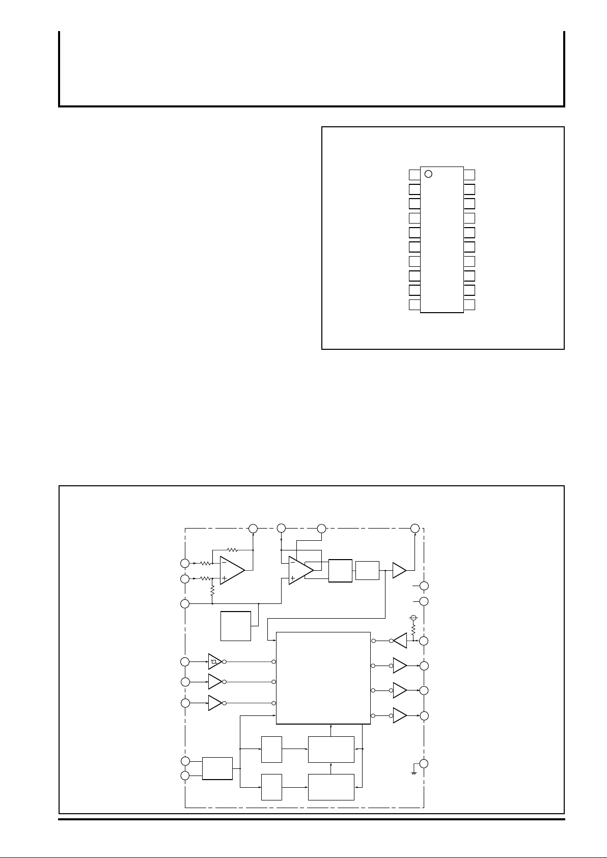
PIN CONFIGURATION(TOP VIEW
→
Read control input
F2F output
Noise filter
Differentiator input
Amplifier output
Amplifier (–) input
Amplifier (+) input
Standard voltage
output
Grounding
LDI
NC
F2F
PKO
PKI
AMP
HD2
HD1
VRF
GND
1
2
←
3
4
→
←
→
→
9
20
19
18
M56710FP
17
165
156
147
138
12
1110
Outline 20P2N-A
• I/O discrimination
Let the data bit time width of a data bit be TBn, and if there is one
next FC between the FC at the end of that bit (i.e. the beginning
of the next bit) to 5/7TBn, let the next bit (Bn+1) be data “1”, and,
if there is no FC, be data “0”.
• Output signal time width
When letting the oscillation cycle of oscillation circuit be TOSC,
• RCP output pulse width TOW•••••••••••••••••••••••about 16TOSC
• RCP delay time to RDT•••••••••••••••••••••••••••••••about 8TOSC
VCC1
VCC2
CX1
CX2
←
IB1
←
IB2
←
INV
→
CLS
→
RDT
→
RCP
Power supply
Power supply
Oscillation capacitor
Oscillation capacitor
Ignore bit 1
Ignore bit 2
Invert input
Card travelling
signal output
Read data output
Read clock output
NC: no connection
BLOCK DIAGRAM
Amplifier (-) input
Amplifier (+) input
e output
Read control input
Ignore bit 2
HD2
HD1
VRFReference volta
LDI
IB2
IB1Ignore bit 1
CX2Oscillation capacito
CX1Oscillation capacitor
Amplifier
output
7
8
9
Reference
voltage
circuit
1
15
16
17
Oscillation
circuit
18
AMP
OP1
T
OSC
Differentiator
input
6
1/5
1/7
PKI
5
OP2
Control circuit
5T
OSC
7TOSC
Noise filter
PKO
4
Sensitivity
setting
11 bit
downcounter
11 bit
upcounter
Waveform
shaping
F2F output
F2F
3
20
19
14
13
12
11
10
Power supply
VCC1
V
CC2
Power supply
INV
Invert input
CLS
Card travelling signal output
RDT
Read data output
RCP
Read clock output
GND
Page 2
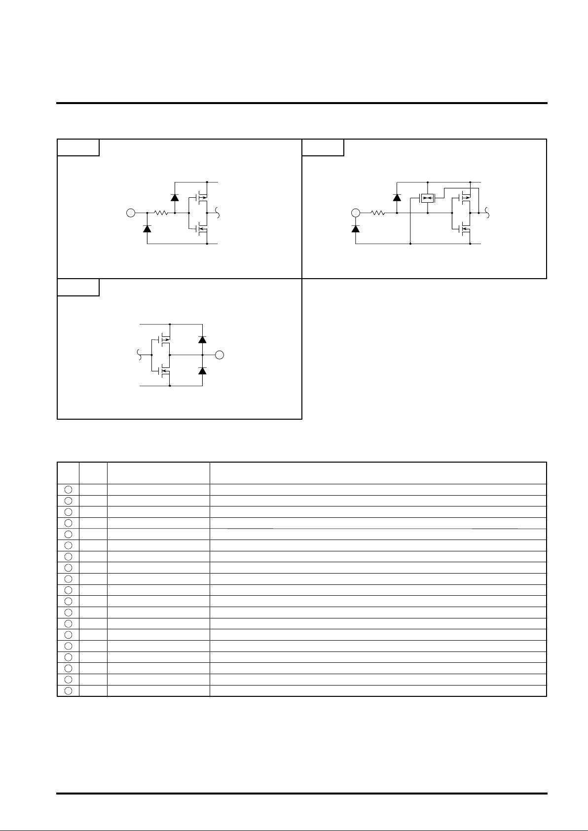
I/O CIRCUIT
MITSUBISHI <CONTROL / DRIVER IC>
M56710FP
F2F MAGNETIC STRIPE ENCORDING CARD READER
1 2
3
LDI, IB1, IB2 input circuit INV input circuit
CC2
V
LDI
IB1
IB2
GND
CLS, RDT, RCP output circuit
VCC2
CLS
RDT
RCP
GND
INV
V
CC2
GND
PIN FUNCTION DESCRIPTION
Pin
No.
10
11
12
13
14
15
16
17
18
19
20
Pin
name
1
LDI
Read control input
3
F2F
F2F output
4
PKO
Noise filter
5
PKI
Differentiator input
6
AMP
Amplifier output
7
HD2
Amplifier (–) input
8
HD1
Amplifier (+) input
9
VRF
Reference voltage output
GND
Grounding
RCP
Read clock output
RDT
Read data output
CLS
Card travelling signal output
INV
Invert input
IB2
Ignore bit 2
IB1
Ignore bit 1
CX2
Oscillation capacitor
CX1
Oscillation capacitor
V
Power supply
CC2
Power supply
VCC1
Name Function
Schmidt trigger input. At “L”, reset the internal digital circuit. At “H”, F2F modulation is possible.
F2F signal output that has amplified, differentiated and further waveform-shaped the magnetic head signal.
Connect noise removing capacitor CNF between PKI and PKO.
Refer to PKO and AMP.
Connect resistor RPK and capacitor CPK between AMP and PKI.
Connect magnetic head between HD1 and HD2.
Connect magnetic head between HD1 and HD2.
Reference voltage output of Vcc 1/2
Clock pulse output after F2F modulation
Data output after F2F modulation
Signal output indicating that card is travelling
CLS, RDT and RCP output becomes “L” active at “H” (OPEN), and “H” active at “L”.
Glance-over bit setting pin
Glance-over bit setting pin
Connect capacitor C
Connect capacitor C
OSC between CX1 and CX2 to set oscillation frequency.
OSC between CX1 and CX2 to set oscillation frequency.
Digital circuit section power supply pin. Supply voltage is Vcc.
Analog circuit section power supply pin. Supply voltage is Vcc (same voltage as Vcc
2).
Page 3
F2F MAGNETIC STRIPE ENCORDING CARD READER
”
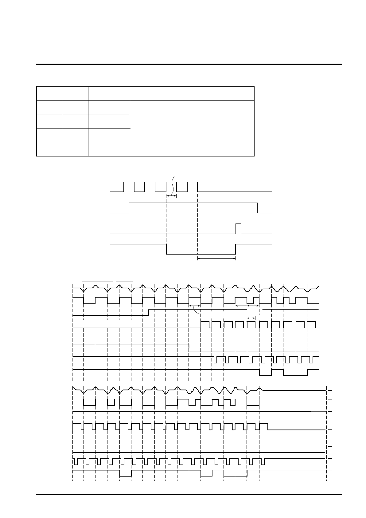
GLANCE-OVER BIT SETTING AND TIMING BY IB1 AND IB2
IB2 input IB1 input
LL
LH
HL
Number of
glance-over bits
4
8
16
Description
• Internal digital circuit is reset with LDI input at “L”.
• LDI input may be at “H” at all times.
• CLS output turns to “L” after counting the flux change
FC (change in the status of F2F) of the number of
glance-over bits, and returns to “H” when BIC (bit
interval counter) has fully counted. (At “L” active).
MITSUBISHI <CONTROL / DRIVER IC>
M56710FP
HH
——
• IB2, IB1: “L”, “L”
x1234
F2F
LDI
BIC
full count
CLS
OPERATING TIMING DIAGRAM
INV : “H”
HD2 - HD1
F2F
LDI
(5/7)
IB2, IB1 : “L”, “L
Bit 1/0 discrimination signal
TBO : Reference bit
About 14300 T
TB0 TBn
Reference bit
OSC
TBn+
5/7TBn
CLS
RCP
RDT
HD2 - HD1
F2F
LDI
(5/7)
CLS
RCP
000 0 100000010110 0
RDT
0000 10110
RDT data is output 1 bit behind F2F data.
Page 4

MITSUBISHI <CONTROL / DRIVER IC>
)
)
F2F MAGNETIC STRIPE ENCORDING CARD READER
ABSOLUTE MAXIMUM RATINGS(Ta = -20 – 75°C, unless otherwise noted
M56710FP
Symbol Parameter Conditions
VCC
VI
VI
IO
VID
Topr
Tstg
Supply voltage
Input voltage
Input voltage
Output voltage
Differential input voltage
Operating temperature
Storage temperature
V
CC1, VCC2
LDI, IB1, IB2, INV
HD1, HD2
CLS, RDT, RCP
Between HD2 and HD1 pins
Ratings
-0.3 – +6.5
-0.3 – V
-0.3 – V
-10 – +10
-1.2 – +1.2
-20 – 75
-55 – 125
CC+0.3
CC+0.3
Note 1: Voltage is based on GND pin of the circuit (0V), unless otherwise noted.
2: Direction of the current flowing into the circuit is represented by “positive” (without code) and that flowing out of the circuit by
“negative” (- code).
RECOMMENDED OPERATING CONDITION(Ta = -20 – 75°C, unless otherwise noted
Symbol Test conditions UnitParameter
CC Supply voltage 5 5.5
V
VI
VIH
VIL
IOH
IOL
VIN
fIN
fOSC
COSC
COSC
RPK
CPK
CNF
RPF
C
VC
CVR
–
Input voltage
“H” input voltage
“L” input voltage
“H” output current
“L” output current
Differential input voltage
Input frequency
Oscillation frequency
External capacitor
External capacitor
External resistor
External capacitor
External capacitor
External resistor
–
External capacitor
External capacitor
VCC1, VCC2
LDI
IB1, IB2, INV
IB1, IB2, INV
CLS, RDT, RCP
CLS, RDT, RCP
HD2-HD1
HD2-HD1
CX1, CX2
CX1, CX2
AMP
PKI
PKI, PKO
PKI, F2F
V
CC1, VCC2
VRF
VCC1 and VCC2 shall have the identical voltage.
fOSC = 1/TOSC
OSC ∞ 1/COSC
f
Reference value when corresponding to 210BPI
Reference value when corresponding to 210BPI
Reference value when corresponding to 210BPI
Reference value
Reference value
Reference value
Reference value
0.8V
Limits
Min. Typ. Max.
4.0
0
CC
0
-0.5
0
3
0.3
0.2
25
33
470
0.033
220
4.7
–
0.1
10.8 2
CC
V
VCC
0.2VCC
0
5
80
15
2
100
Unit
V
V
V
mA
V
°C
°C
V
V
V
V
mA
mA
mVp-p
kHz
MHz
pF
pF
Ω
µF
pF
MΩ
µF
µF
Page 5

MITSUBISHI <CONTROL / DRIVER IC>
)
M56710FP
F2F MAGNETIC STRIPE ENCORDING CARD READER
ELECTRICAL CHARACTERISTICS(Ta = -20 – 75°C and VCC = 5V, unless otherwise noted
Symbol UnitParameter
VTH
VOL CLS, RDT, RCP
OH CLS, RDT, RCP
V
IIL LDI, IB1, IB2
IIL INV
IIH LDI, IB1, IB2, INV
IIT+ INV
VREF VRF
GV11 OP1
GV21 OP1
RIN1 OP1
VOPP1 OP1
IIL2 PKI – F2F
IIH2 PKI – F2F
VTH+2 PKI – F2F
VTH-2 PKI – F2F
VTHD2
Threshold voltage
“L” output voltage
“H” output voltage
“L” input current
“L” input current
“H” input current
Positive threshold current
Reference voltage
Voltage gain 1
Voltage gain 2
Input resistance
Maximum output voltage
“L” sensitivity current
“H” sensitivity current
Positive threshold voltage
Negative threshold voltage
Threshold differential voltage PKI – F2F
IB1, IB2, INV
VPKO Pin voltage range PKO
Test conditions
V
CC = 4 – 5.5V
OL = 10µA
VCC = 4V
CC = 4V
V
V
CC = 5.5V, VI = 0V
V
CC = 5.5V, VI = 0V
V
CC = 5.5V, VI = 5.5V
V
CC = 5.5V, VI = VTH
V
IN = 0mVp-p
I
I
OL = 5mA
I
OH = -10µA
I
OH = -0.5mA
fIN = 1kHz
VIN = 80mVp-p sine wave
f
IN = 15kHz
VIN = 80mVp-p sine wave
IN = 1kHz
f
VIN = 80mVp-p sine wave
IN = 1kHz sine wave
f
THD AMP = 5%
VM, F2F < 0.5V
VM, F2F > 4.5V
On the VRF basis
On the VRF basis
(VTH+2) -
VTH-2
On the VRF basis
IPKI = 1mA – +1mA
VOL3 “L” output voltage F2F VPKI = 0V, IF2F = 0.5mA
VOH3 “H” output voltage F2F VPKI = 5V, IF2F = -0.5mA
VTH+4 Positive threshold voltage LDI
VTH-4 Negative threshold voltage LDI
VHY4 Hysterisis width LDI (VTH+4) - (VTH-4)
ICCW Standby circuit current V
CC1, VCC2 VIN = 0mVp-p
fIN = 8.2kHz
ICCR Operating circuit current V
CC1, VCC2
VIN = 68mVp-p sine wave
fOSC = 1MHz
fOSC Oscillation frequency RCP COSC = 33pF
TOW Output pulse width RCP f
TOD Intra-output delay time RDT, RCP f
OSC = 1MHz
OSC = 1MHz
TNW Input noise width INV
Note: Min. and max. limits do not represent absolute values.
∗
: Typ. limits represent standard values when Ta = 25°C and V
CC = 5V.
Test
circuit
– 0.3V
2
2
2
2
2
2
2
2
1
3
3
3
3
4
4
5
5
–
4
5
5
6
6
–
1
1
1
7
7
7
Min. Typ. Max.
CC – 0.7VCC V
–
–
3.8
3.2
-10
-80
-10
-250
2.3
18
18
7
2
–
0.3
0.2
-0.7
-0.15
-1.2
–
4.5
2.5
1.5
0.5
–
–
0.75
15
7
0.5
Limits
–
–
–
–
–
–
–
–
2.5
20
20
10
–
–
–
0.45
-0.45
–
–
–
–
–
–
–
0.7
1.9
–
16
8
–
∗
0.2
0.4
+10
-10
+10
-50
2.7
24
24
14
-0.3
0.7
-0.2
0.15
1.2
0.5
3.5
2.7
1.5
1.0
2.4
1.5
17
V
V
V
–
V
–
µA
mA
µA
µA
V
Double
Double
kΩ
V
–
P-P
µA
–
µA
V
V
V
V
V
–
V
V
V
V
mA
mA
MHz
µs
9
µs
–
µs
Page 6

MITSUBISHI <CONTROL / DRIVER IC>
M56710FP
F2F MAGNETIC STRIPE ENCORDING CARD READER
TEST CIRCUIT: On the following drawing, COSC = 33pF, RPK=470Ω, CPK = 0.033µF, CNF = 470pF, CVR = 1µF
1. Testingof VREF, ICCW, ICCR, fOSC
VCC
ICCW
ICCR
A
VIN, fIN
VREF
RCP
RPK
CPK
V
CNF
LDI
F2F
PKO
PKI
AMP
HD2
HD1
VRF
GND
TOW
CC1
V
VCC2
CX1
CX2
IB1
IB2
INV
CLS
RDT
RCP
C
OSC
Oscilloscope
fOSC =
fosc
16
TOW
2. Testingof VOL,VOH,IIL,IIH,IIT+
VCC
LDI
F2F
PKO
PKI
AMP
HD2
HD1
CVR
VRF
GND
Note: Short the IB1 and IB2 to the GND when those
V
CC1
VCC2
CX1
CX2
IB1
IB2
INV
CLS
RDT
RCP
C
OSC
pins are not used for testing.
VOL
VOH
I
IIL
IIT+
A
V
IH
VI
IOL
IOH
3. Testingof GV11, GV21, RIN1, VOPP1 4. Testingof IIH2, IIL2, VPKO
VCC
THD meter
VM.AMP
VOPP1
GV11 =
RIN1 =
(ON at VOPP1)
(OFF at RIN)
V
10kΩ
VIN, IIH
VM.AMP
IN
V
2VM.AMP
GV11·VIN - VM.AMP
RPK
CPK
CNF
10kΩ
CVR
x 10(kΩ)
LDI
F2F
PKO
PKI
AMP
HD2
HD1
VRF
GND
CC1
V
VCC2
CX1
CX2
IB1
IB2
INV
CLS
RDT
RCP
LDI
CVR
F2F
PKO
PKI
AMP
HD2
HD1
VRF
GND
C
OSC
VM.F2F
VM.PKO
IPKI
V
IIH2
IIL2
IIL2 is PKI input current providing VM.F2F < 0.5V.
IIH2 is PKI input current providing VM.F2F > 4.5V.
VPKO = VM.PKO - VREF
CC1
V
VCC2
CX1
CX2
IB1
IB2
INV
CLS
RDT
RCP
VCC
C
OSC
Page 7

MITSUBISHI <CONTROL / DRIVER IC>
(
)
(
)
KCLK
M56710FP
F2F MAGNETIC STRIPE ENCORDING CARD READER
5. Testingof VTH+2, VTH-2, VOL3, VOH3
V
VCC2
CX1
CX2
IB1
IB2
INV
CLS
RDT
RCP
VTH+2 = VREF-VPKIVTH-2 = VREF-VPKI+
ON at VOL3 and VOH3
IF2F
VM.F2F
V
VCC
VPKI
“H”
VM.F2F
VOL3
VOH3
VPKI
“L”
0V
5kΩ
CVR
5kΩ
LDI
F2F
PKO
PKI
AMP
HD2
HD1
VRF
GND
VPKI+
VPKI-
CC1
6. Testingof VTH+4, VTH-4
V
CC
COSC
VLDI
VCC
VLDI
“H”
VM.CLS
“L”
LDI
F2F
PKO
PKI
AMP
HD2
HD1
VRF
GND
VTH+4
VTH-4
0V
V
CC1
VCC2
CX1
CX2
IB1
IB2
INV
CLS
RDT
RCP
V
CC
VM.CLS
V
7. Testingof TOW, TOD, TNW
V
CC1
VCC2
CX1
CX2
IB1
IB2
INV
CLS
RDT
RCP
Logic pattern generator
CVR
5kΩ
LDI
F2F
PKO
PKI
AMP
HD2
HD1
VRF
GND
VCC
Oscilloscope
ON at TNW
CL
fosc duty
50%
RCP
RDD
V
INV
0V
RCP
TOW
TOD TOD
CC
Noise input
TNW
TNW, a negative noise put into INV
input, is the maximum time interval not
considered INV input.
Page 8

APPLICATION EXAMPLE
MITSUBISHI <CONTROL / DRIVER IC>
F2F MAGNETIC STRIPE ENCORDING CARD READER
When setting the glance-over bit to 16 bits to let it be “L” active output
5V
VCC1
1
20LDI
M56710FP
RPF
CPK
CVR
CNF
RPK
2
3
F2F
4
PKO
5
PKI
6
AMP
HD2
7
HD1
8
VRF
9
GND RCP
10
V
CC2
CX1
CX2
IB1
IB2
INV
CLS
RDT
19
18
17
16
15
14
13
12
11
CVC
C
OSC
 Loading...