

Page 1
MITSUBISHI <CONTROL / DRIVER IC>
)
4
7
M56694FP/GP
Bi-CMOS & DMOS 32BIT SERIAL-INPUT LATCHED DRIVER
DESCRIPTION
The M56694 is a semiconductor integrated circuit that has a builtin, 32-bit shift register and a latch of CMOS structure with serial
input and serial/parallel output, and a 32-bit totem-pole-type
parallel output driver of high pressure proof DMOS structure.
Employed are Bi-CMOS and high pressure proof DMOS
processing technology.
FEATURES
● Serial input-serial/parallel output
● Cascade connections possible through serial output
● Latch circuit included for each stage
● Driver section supply voltage: VH=120V
● Operating temperature: -20 – 75°C
APPLICATION
Vacuum Fluorescent Display ANODE DRIVER
FUNCTION
The M56694 comprises a 32-bit D type flip-flop with 32 latches
connected to its output.
In accordance with truth table 1, inputting data to SIN and clock
pulse to CLK allows SIN signal to be put into the internal shift
register when the clock changes from “H” to “L”, and
simultaneously shift register data to be shifted sequentially.
Serial output SOUT is used by connecting to the next stage
M56694 SIN when more than one M56694 is used to expand bits
in the series.
In accordance with truth table 2, parallel output allows the latch to
pass data through if LAT input is turned to “H”, and data to be
retained if LAT input is turned to “L”. Driver output HVOn allows
data from the latch to be output if BLK input is turned to “L”, and “L”
to be output if BLK input is turned to “H”, irrespective of data from
the latch.
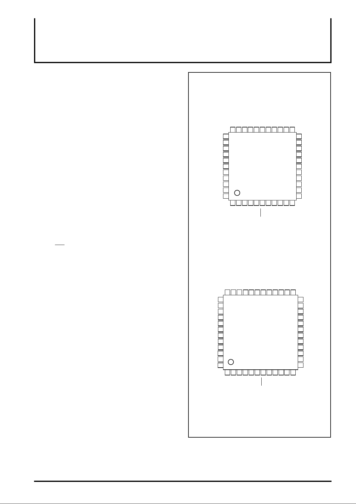
PIN CONFIGURATION(TOP VIEW
HVO12
HVO13
HVO14
HVO15
HVO16
HVO17
HVO18
HVO19
HVO20
3332313029282726252423
34
HVO11
35
HVO10
36
HVO 9
37
HVO 8
38
HVO 7
HVO 6
HVO 5
HVO
HVO 3
HVO 2
HVO 1
N.C
HVO11
HVO10
HVO 9
HVO 8
HVO
N.C
HVO 6
HVO 5
HVO 4
HVO 3
39
40
41
42
43
44
N.C
36
37
38
39
40
41
42
43
44
45
46
47
48HVO 2
123456789
HVO 1
M56694FP
123456789
VH
PGND
SIN
BLK
LAT
CLK
N.C
LGND
Outline 44P6N-A (FP)
HVO12
HVO13
HVO14
HVO15
HVO16
HVO17
HVO18
HVO19
35
34
333231302928272625
M56694GP
H
V
PGND
SIN
BLK
LAT
CLK
VDD
LGND
HVO21
DD
V
HVO20
10
SOUT
HVO22
10
11
H
V
SOUT
HVO21
HVO22
11
VH
22
21
20
19
18
17
16
15
14
13
12
24
23
22
21
20
19
18
17
16
15
14
13
12
PGND
HVO23
HVO24
HVO25
HVO26
HVO27
HVO28
HVO29
HVO30
HVO31
HVO
PGND
N.C
N.C
HVO23
HVO24
HVO25
HVO26
HVO27
HVO28
HVO29
HVO30
HVO31
HVO
32
32
Outline 48P6D-A (GP)
N.C: no connection
Page 2
Bi-CMOS & DMOS 32BIT SERIAL-INPUT LATCHED DRIVER
↓
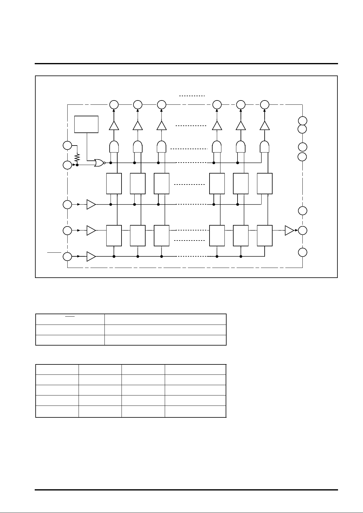
BLOCK DIAGRAM (Note : Pin No. in paretheses are of M56694GP)
(48)
Q
(47)
Q
Q
VDD
BLK
(9)
(5)
(1)
Output
protect
circuit
9
4
(15)
MITSUBISHI <CONTROL / DRIVER IC>
M56694FP/GP
HVO32HVO31HVO30HVO 3HVO 2HVO 1
(14)
14
13
(13)
2
VH
11
(3)(11)
1
PGND
(2)(12)
12
Q
Q
15424344
Q
LAT
SIN
CLK
(6)
(4)
(7)
L
5
3
D
T
6
L
D
Q
D
Q
D
T
TRUTH TABLE
Truth table 1. Shift register section
CLK
H or L
Shift register operation
Truth table 2. Latch and driver sections
L
D
Q
D
T
DATA is shifted.
No changes.
L
D
T
L
D
Q
D
T
L
D
Q
D
LGND
7
(8)
Q
D
T
10
SOUT
(10)
8
N.C
(23)(24)(36)
(37)(43)
HVOnDn LAT BLK
X
H
L
X
X
H
H
L
H
L
L
L
Output all “L”
H
L
Latch’s data output.
Dn=nth bit DFF retention data
HVOn=nth bit driver output
L=“L” level
H=“H” level
X=“L” level or “H” level
Page 3

MITSUBISHI <CONTROL / DRIVER IC>
M56694FP/GP
Bi-CMOS & DMOS 32BIT SERIAL-INPUT LATCHED DRIVER
PIN FUNCTION DESCRIPTION
Pin name
VDD
LGND
V
H
PGND
CLK
SIN
SOUT
LAT
BLK
HVO1 – 32
Logic stage supply voltage
Logic stage ground
Output stage supply voltage
Output stage ground
Clock input for the internal shift resister. The data enter the internal shift resisters and the data in the shift registers wil
shifted in order by High to Low change of the clock.
Serial data input
Serial data output
Latch input. When the LATCH is set to “H”, the data in the shift resister will enter the each latch circuit.
When the LATCH input is set to “L”, the data will be held.
Enable input for output control. When the BLK input is set to “L”, data in the latch circuit will appear at outputs.
When the BLK input is set to “H”, all outputs will be set to “L”.
Output driver (push-pull)
ABSOLUTE MAXIMUM RATINGS (Ta=25°C, unless otherwise noted)
Symbol Ratings
DD
V
H
V
VI
O -0.3 – VDD+0.3
V
V
HVO
Pd
Tstg
Logic stage supply voltage
Output stage supply voltage
Logic inputs voltage
Logic outputs voltage
Output voltage
Power dissipation range
Storage temperature range
Parameter Conditions
Data output
High supply voltage output pin
Ta ≤ 25°C
Function
-0.3 – 7
-0.3 – 120
-0.3 – V
-0.3 – V
940
-55 – 150
DD+0.3
H
l be
Unit
V
V
V
V
V
mW
°C
RECOMMENDED OPERATING CONDITIONS
Symbol
V
DD 4.5 – 5.5
VH
Topr
Supply voltage
Supply voltage
Operating temperature
Parameter Conditions
Ratings Unit
10 – 110
-20 – 75
ELECTRICAL CHARACTERISTICS (VDD=5V, VH=110V and Ta=25°C, unless otherwise noted)
Symbol
IDD
IH
IIH
IIL
HVOH
V
HVOL
V
OH
V
VOL
I
HVOH
IHVOL
TH
V
VTL
Parameter
Supply current 1
Supply current 2
“H” input current
“L” input current
Driver output voltage
Logic output voltage
“H” output current
“L” output current
Output protect operating voltage
Test conditions
No load
Output all “L”, no load
Output all “H”, no load
IH=5V Input pin
V
V
IL = 0V
I
HVOH = -0.5mA
I
HVOL = 0.5mA
I
OH = -0.1mA
I
OL = +0.1mA
SIN, LAT, CLK
BLK
High supply voltage output pin
High supply voltage output pin
Limits
Min. Typ. Max.
1
0
2
02
0
-20
100
106
0.7
4.95
4.5
0.04
-1
1
3.4
3.1
2
50
4
-2
-100
2
0.4
-3
3
V
V
°C
Unit
mA
µA
mA
µA
µA
µA
V
V
mA
mA
V
V
Page 4

MITSUBISHI <CONTROL / DRIVER IC>
M56694FP/GP
Bi-CMOS & DMOS 32BIT SERIAL-INPUT LATCHED DRIVER
SWITCHING CHARACTERISTICS (VDD=5V, VH=110V and Ta=25°C, unless otherwise noted)
Symbol Test conditions Unit
fCLK
t PLH(SO)
t PHL(SO)
tPLH(OUT)
tPHL(OUT)
t rout
t fout
Clock frequency
Logic output propagation time
Driver output propagation time
Driver output rise and fall time
Parameter
Duty = 45 – 55%
CL = 15pF
RO = 220KΩ
CO = 50pF
TEST CIRCUIT
VHVDDinput
(1) Pulse generator characteristics
tr≤20ns tf≤20ns
(2) Capacitance CL includes connection
SOUT
PG DUT CL
HVOn
floating capacitance and probe input
capacitance.
: RO=220KΩ
: CO=50pF
Limits
Min. Typ. Max.
8
120
100
0.16
1.3
0.35
300
300
1
2
1
2.5
2
MHz
ns
ns
µs
µs
µs
µs
50Ω
TIMING WAVEFORM
CLK
SIN
SOUT
BLK
50%
90%
50%
tPHL(SO)
CO RO
1/fmax
50%
50% 50%
50%
thtsu
tfso trso
10%
10%
tPLH(SO)
50%
50%
90%
50%
HVOn
tr
10%
tPLH(OUT)
OUT
90%
50%
90%
tPHL(OUT)
50%
tfOUT
10%
Page 5

TYPICAL CHARACTERISTICS
MITSUBISHI <CONTROL / DRIVER IC>
M56694FP/GP
Bi-CMOS & DMOS 32BIT SERIAL-INPUT LATCHED DRIVER
0.94
Power dissipation Pd(W)
10
Output current IOH(mA)
Thermal derating
1.0
0.5
0
0
Temperature Ta(°C)
Duty cycle vs Permissible
output current
9
8
7
6
5
4
3
2
1
0
0
40
Duty cycle (%)
Driver output VON–IOH
10
Ta=+75°C
8
Ta=+25°C
6
Ta=-20°C
4
2
“H” output current IOH(mA)
0
100755025
0246810
“H” output voltage V
ON(V)
Duty cycle vs Permissible
output current
–
1
13
14
16
24
32
8020 100
60
10
Output current IOH(mA)
9
8
7
6
5
4
3
2
1
0
20
0
40
80
60
Duty cycle (%)
100
–
1 8
9
16
24
32
•Ta=25°C
Note •Ta=75°C
•Repeated frequency >100Hz
•Figure in the circle represents the number of
concurrently operating output circuits.
•Current value denotes a numerical value per circuit.
1. VDD=5V and VH=110V, unless otherwise noted
Note
Note
•Repeated frequency >100Hz
•Figure in the circle represents the number of
concurrently operating output circuits.
•Current value denotes a numerical value per circuit.
2. Thermal derating characteristics represent those of an individual IC unit.
3. Allowable duty cycle output current characteristics represent that when a standard
substrate is mounted. (Standard substrate: 70x70x1.6mm glass epoxy)
 Loading...