

Page 1
MITSUBISHI <CONTROL / DRIVER IC>
M54975P/FP
Bi-CMOS 8-BIT SERIAL-INPUT LATCHED DRIVER
DESCRIPTION
The M54975 is a semiconductor integrated circuit fabricated using
Bi-CMOS technology. It contains a serial input to serial/parallel
output 8-bit CMOS shift register and CMOS latch as well as bipolar
8-bit parallel-output driver.
FEATURES
● Serial input to serial/parallel output
● Cascade connections possible through serial output
● Latch circuit included for each stage
● Enable input for output control
● Low supply current .................................. ICC ≥ 10µA at standby
● Serial input/output level is compatible with standard CMOS
● Driver : Withstand voltage ...................................... BVCEO ≥ 30V
Large drive current ................................ (IO(max)=300mA)
● Wide operating temperature range ..................... Ta=-20 – +75°C
APPLICATION
Thermal printer head dot driver, Serial-to parallel conversion, Relay
and Solenoid driver
FUNCTION
The M54975 consists of an 8-bit D-type flip-flop, the output of
which is connected to 8 latches.
When data is applied to the serial data input (S-IN) and a clock
pulse is applied to clock input (T), an “L” to “H” change of the clock
will cause the data input signals to enter the internal shift registers
and the data in the shift registers will be shifted in order.
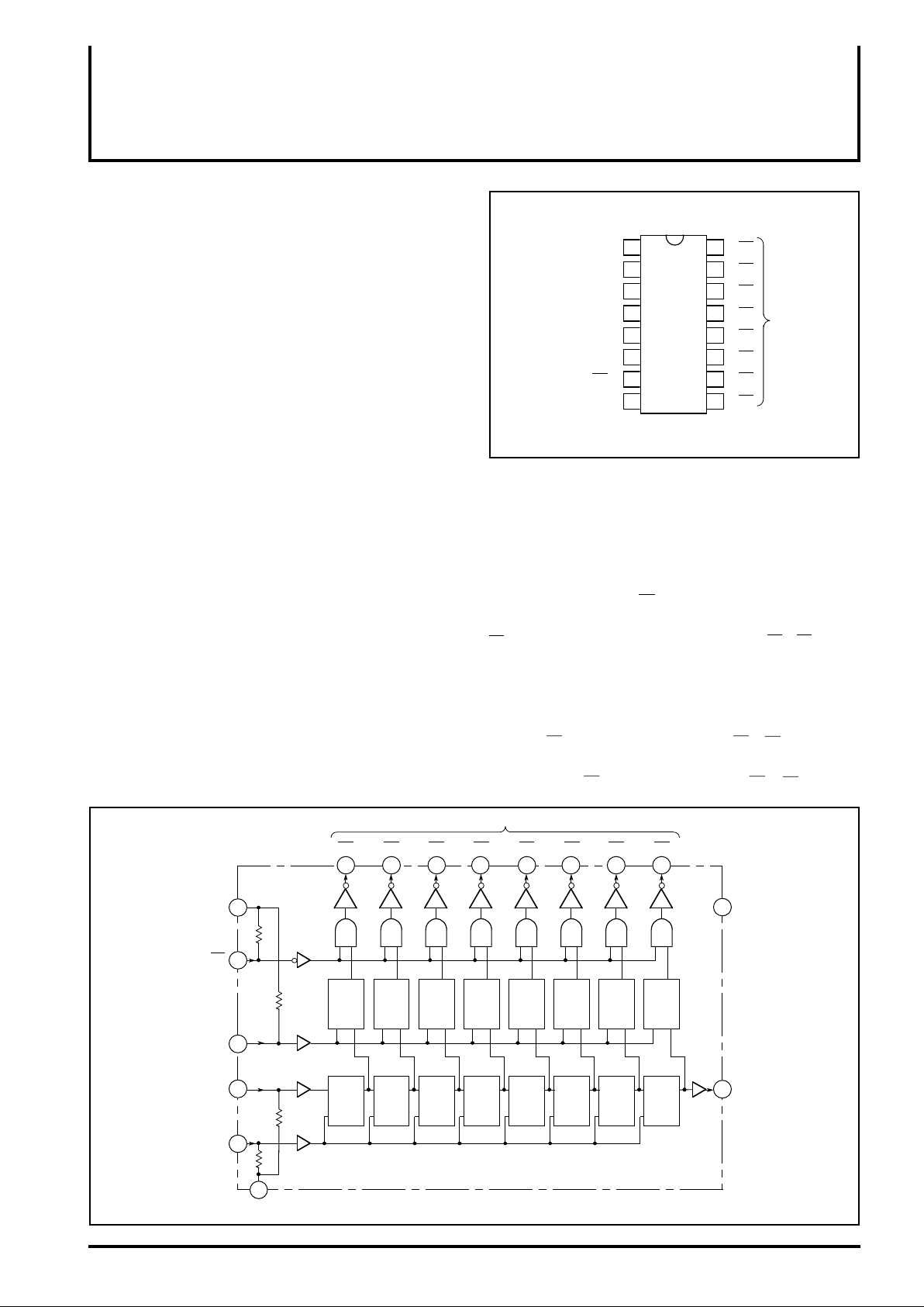
PIN CONFIGURATION (TOP VIEW)
S-IN
L-GND
V
S-OUT
LATCH
EN
P-GND
T
→
1
→
2
3
M54975P
CC
4
←
→
Outline
16P4(P)
O1
→
16
O2
→
15
O3
→
14
→
O4
13
→
125
→
116
→
107
→
98
Parallel outputs
O5
O6
O7
O8
16P2N-A(FP)
Clock
Serial input
Logic GND
Serial output
Latch input
Enable input
Driver GND
Using a number of M54975 units for bit expansion in series will
entail connecting serial output (S-OUT) to S-IN of the next-stage
M54975.
In parallel output, when the latch input is set to “H” and the outputcontrol input (enable input EN) is “L”, a clock pulse changing from
“L” to “H” will cause the serial data input signal to appear at output
O1, and the data will be shifted in order at outputs O2 – O8.
The parallel output will yield a signal that is inverted with respect to
the serial data input.
Setting the LATCH input to “L” will prevent data from entering the
latch.
When the EN input is set to “H”, all outputs (O1 – O8) will be set to
OFF. Since the internal logic state of the IC is uncertain at poweron time, set the EN input to “H” (and outputs O1 – O8 will set to
BLOCK DIAGRAM
Power supply
CC
V
ENEnable input
LATCHLatch input
S-INSerial input
Parallel outputs
O1
O2
O3
O4
O5
O6
O7
O8
16
15 14 13 12 11 10 9
4
7
Q
Q
Q
Q
Q
Q
Q
Q
L D
L D
L D
L D
L D
L D
L D
L D
6
2
TClock
1
3
L-GND
Logic GND
QTD
QTD
QTD
QTD
QTD
QTD
QTD
QTD
8
5
Driver GNDP-GND
Serial outputS-OUT
Page 2
MITSUBISHI <CONTROL / DRIVER IC>
M54975P/FP
Bi-CMOS 8-BIT SERIAL-INPUT LATCHED DRIVER
OFF) until the input data is set and the internal logic state has been
determined.
L-GND is the ground of the CMOS logic circuit section and P-GND
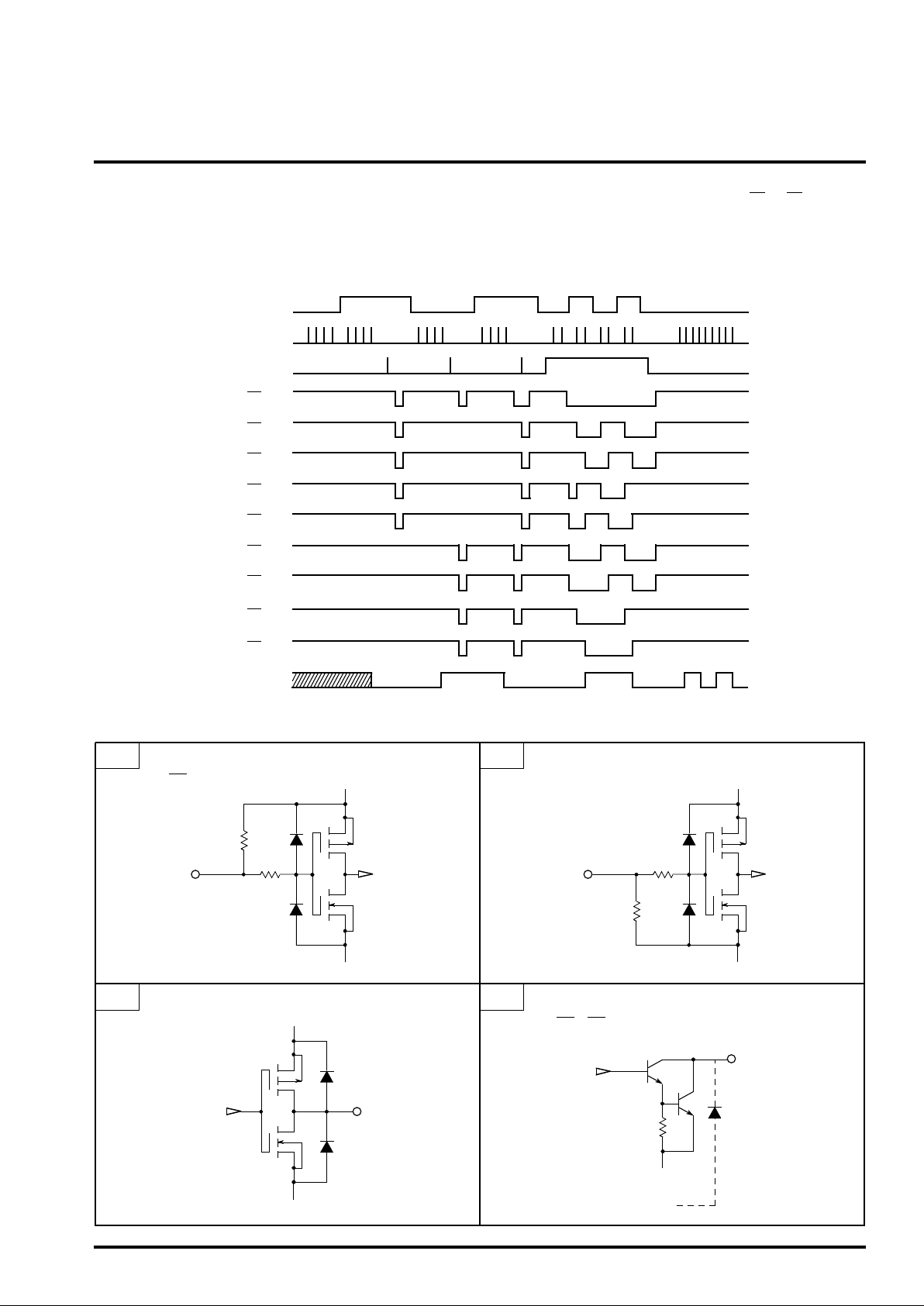
TIMING CHART
S-IN
T
LATCH
EN
O1
O2
O3
O4
O5
O6
O7
O8
is the ground for the output driver section (O1 – O8), which is
made up of bipolar transistors that are capable of driving large
currents.
S-OUT
*
The state of the shaded part is unstable.
INPUT/OUTPUT CIRCUIT DIAGRAM
1
3 4
Inputs with pullup resistor
(EN, LATCH)
RIN
Serial output
(S-OUT)
VCC
VCC
L-GND
2
Inputs with pulldown resistor
(T, S-IN)
RIN
VCC
L-GND
Parallel outputs
(O1 – O8)
1.5kΩ
L-GND
P-GND
L-GND
Page 3

Bi-CMOS 8-BIT SERIAL-INPUT LATCHED DRIVER
ABSOLUTE MAXIMUM RATINGS (Ta=-20 to 75°C)
Symbol Ratings UnitParameter Conditions
MITSUBISHI <CONTROL / DRIVER IC>
M54975P/FP
VCC
VI
VO
IO
Pd
Topr
Tstg
Supply voltage
Input voltage
Output voltage
Output current
Power dissipation
Operating temperature
Storage temperature
S-OUT
O1 – O8 : OFF
O1 – O8 : ON
T
a=25°C
M54975P
M54975FP
RECOMMENDED OPERATING DONDITION
Symbol
VCC
VO
IO
Parameter
Supply voltage
Applied output voltage
Output current (per circuit)
O1 – O8 : OFF
M54975P
M54975FP
Conditions
ELECTRICAL CHARACTERISTICS (Ta=25°C, VCC=5V, unless otherwise noted)
Symbol
VIH
VIL
IN
R
VOH
VOL
IOH
IOL
VOL1
VOL2
VOL3
IOLK
ICC1
ICC2
High-level input voltage
Low-level input voltage
Input resistance
High-level output voltage
Low-level output voltage
High-level output current
Low-level output current
Low-level output voltage
Output leak current
Supply current
S-OUT
S-OUT
S-OUT
S-OUT
O1 – O8
O1 – O8
T
a=-20 – 75°C
|IO|≤1µA
OH=4.5V
V
VOL=0.4V
OL=100mA
I
I
OL=200mA
OL=300mA
I
O=30V
V
Input: open, All driver outputs: OFF
One driver output is ON.
Test conditions
-0.5 – +8
-0.5 – V
CC+0.5
-0.5 – V
CC+0.5
-0.5 – +30
350
1.25
0.8
-20 – 75
-55 – 125
Limits
Min. Typ. Max.
456
30
300
100
Limits
Min. Typ. Max.
0.7V
CC
0
50
4.9
—
-100
400
—
—
—
—
—
—
CC
V
0.3VCC
—
—
0.1
—
—
1.2
1.4
1.6
50
10
1.7
V
V
V
mA
W
°C
°C
Unit
V
V
mA
UnitParameter
V
V
kΩ
V
V
µA
µA
V
V
V
µA
µA
mA
TIMING REQUIREMENTS (Ta=-20 to 75°C, unless otherwise noted)
Symbol
f(T)
tw(T)
tw(L)
tsu
th
td(T-L)
tr(T)
tf(T)
Parameter
Clock frequency
Clock pulse width
Latch pulse width
Data setup time
Data hold time
Clock-latch time
Clock pulse rise time
Clock pulse fall time
Input duty: 40 – 60%
Test conditions
Limits
Min. Typ. Max.
2
200
200
100
100
400
500
500
Unit
MHz
ns
ns
ns
ns
ns
ns
ns
Page 4

TIMING CHART
MITSUBISHI <CONTROL / DRIVER IC>
M54975P/FP
Bi-CMOS 8-BIT SERIAL-INPUT LATCHED DRIVER
Serial input
Clock
Latch input
S-IN
LATCH
2.5V
tsu
T
t
h
2.5V 2.5V
t
w
(T) tr(T)
t
d
(T-L)
2.5V
2.5V 2.5V
t
w
(L)
10%
SWITCHING CHARACTERISTICS (Ta=25°C, VCC=5V, unless otherwise noted)
Symbol Test conditions
tPLH
tPHL
tPLH
tPHL
tPLH
tPHL
Low-to-high-level output propagation time
From input T to output S-OUT
High-to-low-level output propagation time
From input T to output S-OUT
Low-to-high-level output propagation time
From input T to output O
High-to-low-level output propagation time
From input T to output ON
Low-to-high-level output propagation time
From input EN to output ON
High-to-low-level output propagation time
From input EN to output ON
Parameter
N
VIH=5V
VIL=0V
RL(S-OUT)=∞
RL(ON)=100Ω
(N=1–8)
CL=15pF
90%
90%
t
f
10%
(T)
Limits
Min. Typ. Max.
0.3
0.3
10
2
10
2
Unit
µs
µs
µs
µs
µs
µs
TEST CIRCUIT
PG
TIMING CHART
Serial output
Enable input
Output
Clock
Input
50Ω
S-OUT
EN
ON
V
M54975P/FP
T
CC
The input waveform: tr ≤ 20ns, tf ≤ 20ns
The capacitance C
and probe input capacitance.
2.5V
tPHL
2.5V
2.5V
L includes the wiring stray capacitance
2.5V
2.5V
tPLHtPHL
2.5V
t
PHL
2.5V
2.5V
tPLH
RL
Output
CL
2.5V
t
PLH
2.5V
Page 5

Bi-CMOS 8-BIT SERIAL-INPUT LATCHED DRIVER
TYPICAL CHARACTERISTICS (VCC=5V, unless otherwise noted)
MITSUBISHI <CONTROL / DRIVER IC>
M54975P/FP
Thermal derating
(Absolute maximum rating)
1.5
M54975P
1.0
M54975FP
0.5
Power dissipation Pd (W)
0
0
25 50 75 100
Ambient temperature Ta (°C)
Duty cycle vs. allowable output current
(M54975P)
400
300
200
T
a = 25°C
Repetitive frequency >10H
100
Output current Io (mA)
Each figure in a circle shows
the number of output circuits which
operate simultaneously.
Current value : output current per circuit
0
0 20 40 60 80 100
Z
–
1 3
4
5
6
7
8
Driver output VOL vs. IOL
400
Ta = -20°C
OL (mA)
300
Ta = 25°C
Ta = 75°C
200
100
Low-level output current I
0
0 0.5 1.5
1.0
Low-level output voltage VOL (V)
Duty cycle vs. allowable output current
(M54975P)
400
300
200
T
a = 75°C
100
Output current Io (mA)
Repetitive frequency >10HZ
Each figure in a circle shows
the number of output circuits which
operate simultaneously.
Current value : output current per circuit
0
0 20 40 60 80 100
1
2
3
4
5
6
7
8
Duty cycle (%)
Duty cycle vs. allowable output current
(M54975FP)
200
180
160
140
120
100
80
Ta = 25°C
Repetitive frequency >10H
60
Output current Io (mA)
Each figure in a circle shows
the number of output circuits which
40
operate simultaneously.
20
Current value : output current per circuit
CC = 5.5V
V
0
0 20 40 60 80 100
Duty cycle (%)
Z
Duty cycle (%)
Duty cycle vs. allowable output current
(M54975FP)
200
180
160
140
120
– –
1 6
7
8
100
80
T
a = 75°C
Repetitive frequency >10H
60
Output current Io (mA)
Each figure in a circle shows
the number of output circuits which
40
operate simultaneously.
20
Current value : output current per circuit
CC = 5.5V
V
0
0 20 40 60 80 100
Z
Duty cycle (%)
1 4
5
6
7
8
 Loading...