

Page 1
FEATURES
■ 2 DIGIT LED DRIVER (14 segments)
■ CURRENT GENERATOR OUTPUTS (no
registor required)
■ CONTINUOU BRIGHTNESS CONTROL
■ SERIAL DATA INPUT
■ DATA ENABLE
■ WIDE SUPPLY VOLTAGE OPERATION
■ TLL COMPATIBILITY
■ APPLICATION EXAMPLES
■ MICROPROCESSOR DISPLAYS
■ INDUSTRIAL CONTROL INDICATOR
■ RELAY DRIVER
■ INSTRUMENTATI ON READ O U TS
DESCRIPTION
The M5481 is a monolithic MOS integrated circuit
produced with a N-channel silicon gate techn ology. It uses the M54 50 die packaged in a 20-pin
plastic package copper frame, making it ideal for a
1-digit display. A single pin controls the LE D display brightness by setting a reference current
through a variable resistor connected either to
V
DD
or to a separate supply of 13.2V maximum.
The M5481 is a pin-to-pin replacement of the NS
MM 5481.
PIN CONNECTIONS
M5481
LED DISPLAY DRIVER
DIP20
(Plastic package)
ORDER CODE: M54 81 B7
Output Bit 8
Output Bit 7
Output Bit 6
Output Bit 5
Output Bit 4
Output Bit 3
Output Bit 2
Output Bit 1
Brightness Control
V
DD
1
2
3
4
5
6
7
8
9
10
20
19
18
17
16
15
14
13
12
11
Output Bit 9
Output Bit 9
Output Bit 9
Output Bit 9
Output Bit 9
V
SS
Output Bit 9
Data Enable
Data In
Clock
Version 4.1
April 2000 1/8
1
Page 2
M5481
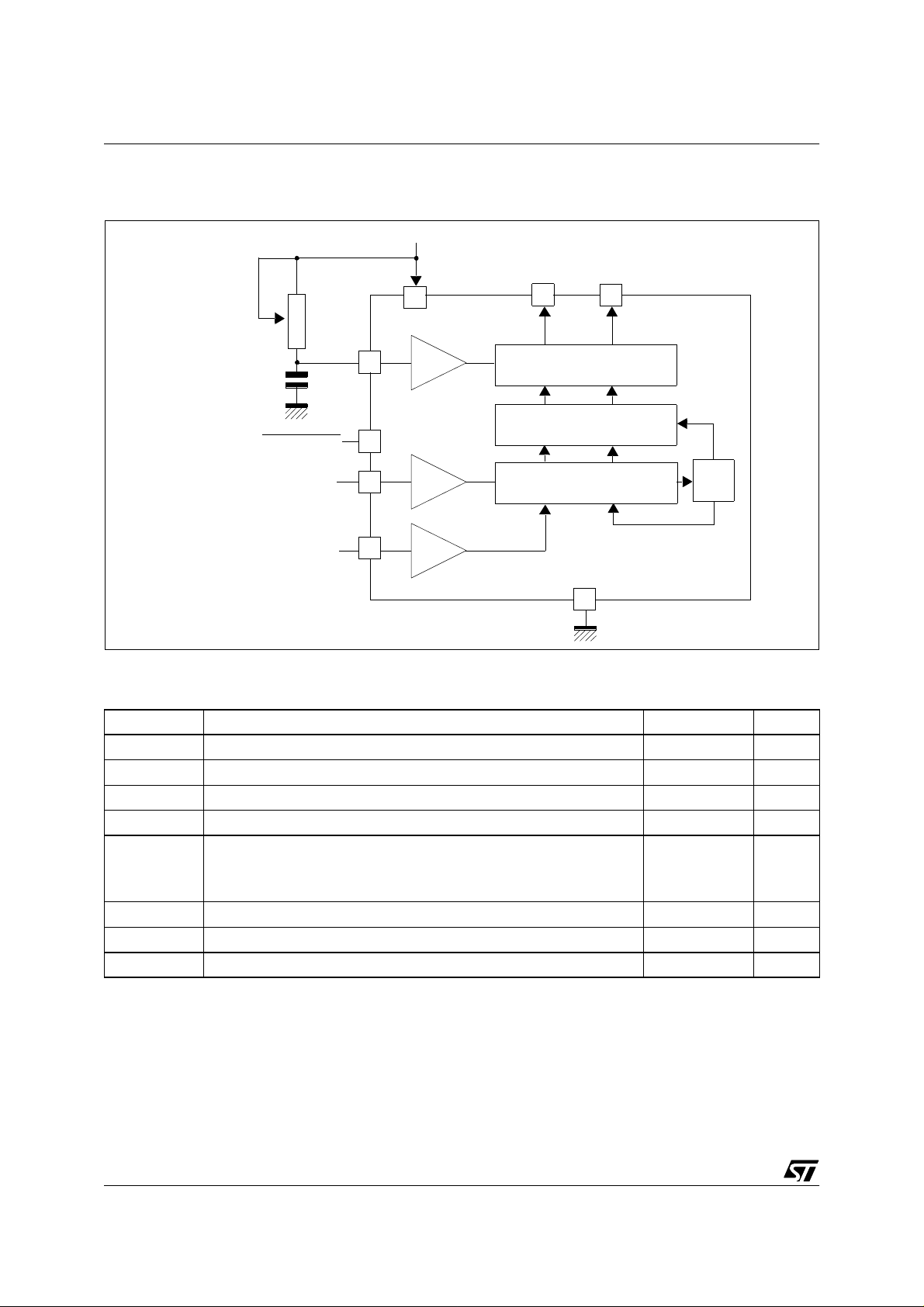
1 - BLOC DIAGRAM
Figure 1.
Brightness
Control
100kΩ
V
10
DD
Output
Bit 14
14
Output
Bit 1
8
9
35 Output Buffers
1nF
Load
Data Enable
Serial Data
Clock
13
12
11
35 Latches
35-Bit Shift Register
Reset
15
2 - ABSOLUTE MAXIMUM RATINGS
Symbol Parameter Value Unit
V
DD
Vi Input Voltage -0.3 to 15 V
Vo(off) Off-state Output Voltage 15 V
Io Output Sink Current 40 mA
Supply Voltage -0.3 to 15 V
Total package power Dissipation
P
tot
T
j
T
oper
T
stg
Stresses exceed ing those list ed under “Ab solute Max imum Rating s” may caus e permanen t damage to the device a nd
affect its reliability.
2/8
Junction Temperatu re 150 °C
Operating Temperature Range -25, +85 °C
Staorage Temperature Range -65, +150 °C
at 25°C
t 85°C
1.5
800
W
mW
2
Page 3
3 - STATIC ELECTRICAL CHARACTERISTICS
(T
within operational range, VDD=4.75V to 13.2V, VSS=0V, unless otherwise specified)
amb
Symbol Parameter Test Conditions Min Typ Max Unit
V
DD
Idd Supply Current V
Supply Voltage 4.5 13.2 V
=13.2V 7 mA
DD
M5481
Input Voltages
Vi
IB Brightness Input Current (Note 2) 0 0.75 mA
VB Brightness Input Voltage (pin9)
Vo(off) Off-state Output Voltage 13.2 V
Io
fclock
Io Output Matching (Note 1)
Note 1 Output matching is calculated as the percent variation from Imax+Imin/2
Note 2 With a fixed resistor on the brightness input some variation in brightness will occur from one device to another.
Note 3 Absolute maximum for each output should be limited to 40mA.
Note 4 the Vo voltage should be regulated by the user.
Logical “0” Level
Logical “1” Level
Output Sink Current (Note 3)
Segment OFF
Segment ON
Input Clock Frequency 0 0.5 MHz
+10µA Input Bias
4.75≤V
V
DD
Input Curren=750µA
T
amb
Vo=3V
Vo=1V (Note 4)
Brightness In.=0µA
Brightness In.=100µA
Brightness In.=750µA
DD
>5.25
=25°C
≤5.25
-0.3
2.2
V
-
DD
2
3 4.3 V
0
2
12
2.7
15
0.8
V
DD
V
DD
10
10
4
25
±20 %
V
V
V
µA
µA
mA
mA
4 - FUNCTIONAL DESCRIPTION
The M5481 uses the M5450 die which is packaged
to operate 2-digit alphanumeric displays with minimal interface with the display and the data source.
Serial data transfer from the data source to the display driver is accom plished with 2 signals, serial
data and clock. using a format of a leadi ng “1” followed by the 35 data bits allows data transfer without an additional load signal.
The 35 data bits are latched after the 36th bit is
complete, thus providing non-multiplexed, direct
drive to the display. Outputs change only if the serial data bits differ from the previous time. Display
brightness is determined by control of the output
current for LED displays. A 1nF capacitor should
be connected to brightness c ontrol (pin 9) to prevent possible oscillations.
A bloc diagram is shown on F igure 1. The output
current is typically 20 times g reater than the current into pin 9, which is set by an external variable
resistor.
The latter is an internal limiting resistor of 400Ω
nominal value.
Figure 2 shows the input data format. A start bit of
logical “1” precedes the 35 bits of data. At the 36th
clock a LOAD is generated synchronously with the
high state of the clock, which l oads the 35 bits of
the shift registers into the latches.
3/8
Page 4

M5481
Figure 2. Input Data Format
1
CLOCK
DATA
LOAD
(INTERNAL)
RESET
(INTERNAL)
START
BIT 1
At the low state of the clock a RESET signal is
generated which clears all the shift registers for
the next set of data. The shift registers are static
master slave configurations. There is no clear for
the master portion of the first shift register, thus allowing continuous operation.
There must be a complete set of 36 clocks or the
shift registers will not clear.
When power is first a pplied t o the chip an internal
power ON reset signal is generated which resets
all registers and all latches. The START bit and the
first clock reset the chip to its normal operation.
Figure 3 shows the timing relationships between
Data, Clock and DATA ENABLE
.
A maximum clock frequency of 0.5MHz is assumed.
Figure 4 shows the Output Data Format for the
M5481. Because it uses only 14 of the possible 35
outputs, 21 of the bits are “Don’t Cares”.
For applications where a lesser number of outputs
are used it is possible to either increase the current per output or operate the part at higher than
1V Vout.
Figure 4. Seri al Bus/ Outputs Co rrespondan ce
36
BIT 34 BIT 35
The following equation can be used for calculations.
Tj=[(Vout)(I
)(No. of segments)+VDDx7mA]
LED
x(80°C/W)+Tamb
where:
Tj=junction temperature (150°Cmax)
Vout= voltage at the LED driver outputs
ILED= LED current
80°C/W=thermal coefficient of the package
Tamb=ambiant temperature
Figure 3.
CLOCK
DATA
300ns (min.)
DATA ENABLE
100ns (min.)
5450 34 33 32 31 30 29 28 27 26 25 24 23 22 21 20 19 18 START
5481 XXXX13XXXXX1211109XXXSTART
5450 1716151413121110987654321START
5481 X8765XXXX4321XXXXSTART
4/8
Page 5

5 - TYPICAL APPLIC ATION
14 SEGMENTS
M5481
DISPLA Y DRIVER
PROCESSO RKEYBOARD
PLL
SYNTHESIZER
LED DISPLAY
BASIC electronically tuned TV system.
6 - POWER DISSIPATION OF THE IC
M5481
The power dissipation of the IC can be limited using different configurations.
+V
C
R
I
D
V
D
V
OU T
In this application R must be chosen by taking into
account the worst operating conditions.
R is determined by the maximum nu mber of segments activated.
VCV
– V
----------------------------------------------------------------=
R
The worst case condition for the device i s when
roughly half of the max imum num ber of segments
are activated.
It must be checked that the total power dissipation
does not exceed the absolute maximum ratings of
the device.
In critical cases more resistors can be used in conjunction with groups of segments. In this case the
current variation in the single resistor is reduced
and P
limited.
tot
DMAX
N
–
MAXxID
OMIN
5/8
Page 6

M5481
+V
C
+V
C
V
OUT+VD
In this configuration the drop on the serial connected diodes is quite stable if the diodes are properly
chosen.
The total power dissipation of the IC depends only,
in first approximation, on the num ber of segm ent s
activated.
In this configuration V
OUT+VD
is constant. the total
power dissipation of the IC depends only on the
number of segments activated.
6/8
Page 7
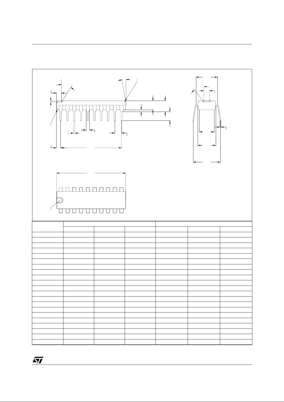
7 - PACKAGE MECHANICAL DATA
20 Pins — Plastic Dip
N
e
K1
K2 R1
Z
N
b
B
e3
D
R1
a1
M5481
N
I
A
L
Tie Bar Center
K
C F
Ee4
b1
R2
Dimensions
20
1
Millimeters Inches
Min. Typ. Max. Min. Typ. Max.
11
10
A 3.25 3.30 3.35 0.128 0.130 0.132
a1 0.508 0.020
B 1.39 1.65 0.055 0.065
b 0.381 0.457 0.533 0.015 0.018 0.021
b1 0.20 0.254 0.30 0.008 0.010 0.012
C 5.20 5.33 5.46 0.205 0.210 0.215
D 24.9 25.15 25.4 0.980 0.990 1.000
E 7.8 8.5 9.1 0.307 0.335 0.358
e 2.29 2.54 2.79 0.090 0.100 0.110
e3 22.60 22.86 23.11 0.890 0.900 0.910
e4 7.36 7.62 7.87 0.290 0.300 0.310
F 6.22 6.35 6.50 0.245 0.250 0.255
I 3.42 3.68 3.93 0.135 0.145 0.155
L 3.17 3.30 3.42 0.125 0.130 0.135
N7d 7d
R1 0.152 0.006
R2 0.762 0.030
K 1.524 0.060
K1 0.762 0.030
K2 0.762 0.030
Z 1.27 1.34 0.050 0.053
7/8
Page 8

M5481
Information furnished is believed to be accurate and reliable. However, STMicroelectronics assumes no responsibility for the con sequences of use of suc h informatio n nor for any infringeme nt of patents or other right s of
third parties whi ch ma y res ult fro m its u se. N o licen se is grant ed by implic ation or oth erwi se und er an y patent
or patent rights of STMicroelectronics. Specifications mentioned in this publication are subject to change without notice. This publication supe rsedes and repl aces all informa tion previously s upplied. STMicr oelectronics
products are not auth orized for use as critical componen ts in lif e support devices or syst ems with out the e xpress written approval of STMicroelectronics.
The ST logo is a registered trademark of STMicroelectronics
2000 STMicroelectronics - All Rights Reserved.
Purchase of I
components in an I
Australia - Brazil - China - Finland - France - Germany - Hong Kong - India - Italy - Japan - Malaysia - Malta - Morocco -
8/8
2
C Components by STMicroelectronics conveys a license under the Philips I2C Patent. Rights to use these
2
C system is granted provided that the system conforms to the I2C Standard Specification as defined
by Philips.
STMicroelectronics Group of Companies
Singapore - Spain Sweden - Switzerland - United Kingdom - U.S.A.
http://www.st.com
3
 Loading...