

Page 1
.
3 1/2 DIGIT LED DRIV ER (23 segment s)
.
CURRENT GENERATOR OUTPUTS (no resistors required)
.
CONTINUOUS BRIGHTNESS CONTROL
.
SERIAL DATA INPUT
.
NO LOAD SIGNAL REQUIRED
.
WIDE SUPPLY VOLTAGE OPERA TION
.
TTL CO MPAT IB ILI TY
Applications examples
.
MICROPROCESSOR DISPLAYS
.
INDUSTRIAL CONTROL INDICATION
.
RELAY DRIVER
.
INSTRUMENTATION READOUTS
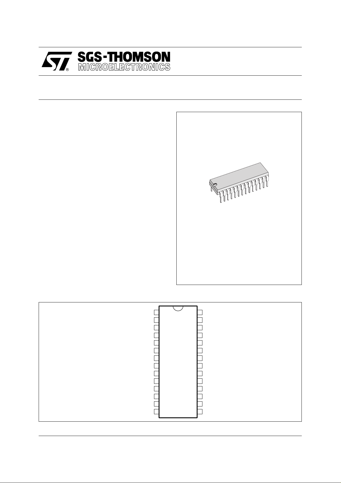
M5480
LED DISPLAY DRIVER
DESCRIPTION
The M5480 is a monolithic MOS integrated circuit
produced with a N-channel silicon gate technology .
It utilizes the M5451 die packaged in a 28-pin
plas-tic package making it ideal for a 3
dispaly . A single pin controls the LED d ispaly brightness by setting a reference current through a variable resistor connected either to V
separate supply of 13.2V maximum.
The M5480 is a pin-to-pin replacement of the NS
MM 5480.
PIN CONNECTIONS
OUTPUT BIT 11
OUTPUT BIT 10
OUTPUT BIT 9
OUTPUT BIT 8
OUTPUT BIT 7
OUTPUT BIT 6
OUTPUT BIT 5
OUTPUT BIT 4
OUTPUT BIT 3
OUTPUT BIT 2
OUTPUT BIT 1
BRIGHTNESS CONTROL
1/2 digit
or to a
DD
V
SS
V
DD
DIP-28
(Plastic Package)
ORDER CODE : M5480B7
1
2
3
4
5
6
7
8
9
10
11
12
13
14
28
27
26
25
24
23
22
21
20
19
18
17
16
15
OUTPUT BIT 12
OUTPUT BIT 13
OUTPUT BIT 14
OUTPUT BIT 15
OUTPUT BIT 16
OUTPUT BIT 17
OUTPUT BIT 18
OUTPUT BIT 19
OUTPUT BIT 20
OUTPUT BIT 21
OUTPUT BIT 22
OUTPUT BIT 23
DATA IN
CLOCK IN
5480-01.EPS
May 1993
1/6
Page 2
M5480
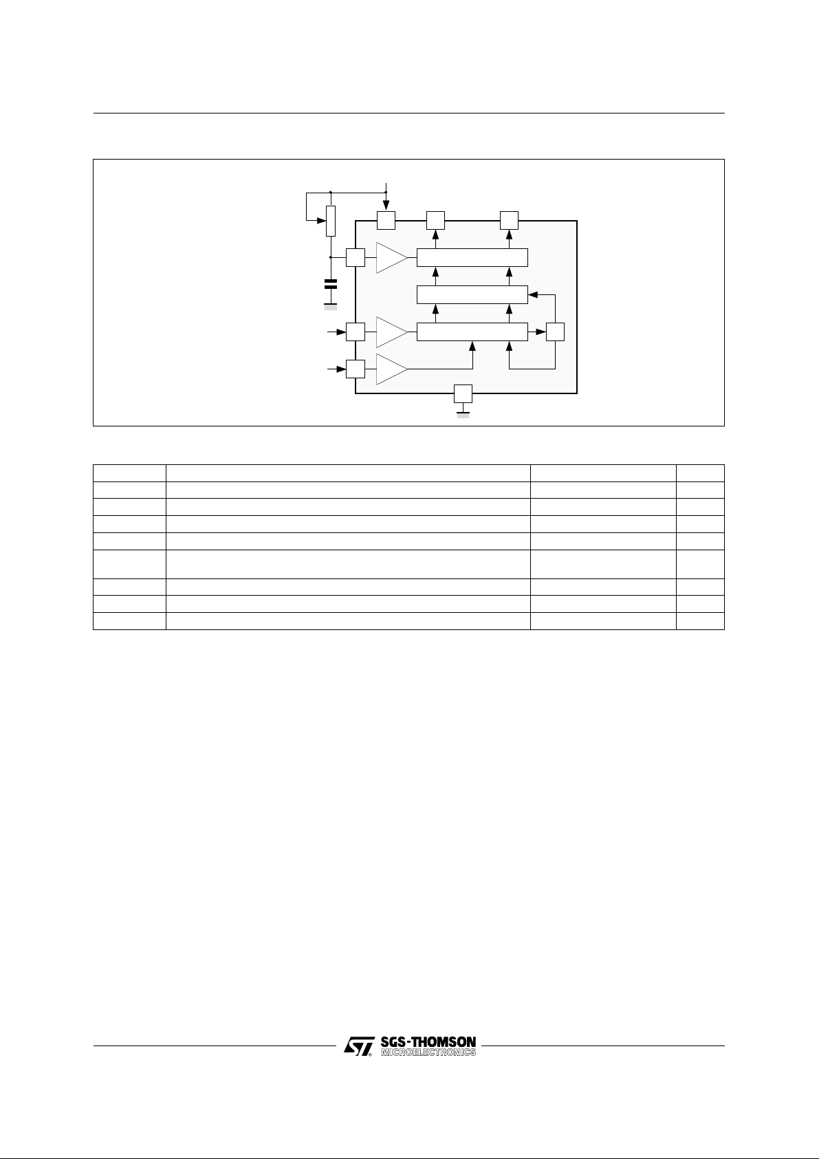
BLOCK DIAGRAM (Figure 1)
BRITGHTNESS
CONTROL
V
14
DD
OUTPUT
BIT 23
OUTPUT
BIT 1
1217
35 OUTPU T BUFERS
35 LATCHES
35 BIT SHIFT REGISTER
LOAD
RESET
1nF
SERIAL
DATA
CLOCK
13
16
15
1
ABSOLUTE MAXIMUM RATINGS
Symbol Parameter Value Unit
V
DD
V
V
O (off)
I
O
P
tot
T
T
oper
T
stg
Stresses in excess of those listed un der "Absolute Maximum Ratings" may cause permanent damage to the device. This is a s tress rating only
and functional operation of the device at these or any other conditions in excess of those in dicated in the operational sect ions of this specifi cation
is not implied. Exposure to absolute maximum rating conditions for extended periods may affect device reliability.
Supply Voltage – 0.3 to 15 V
Input Voltage – 0.3 to 15 V
I
Off State Output Voltage 15 V
Output Sink Current 40 mA
Total Package Power Dissipation at 25 °C
at 85 °C
Junction Temperature 150 °C
j
940
490
Operating Temperature Range – 25, + 85 °C
Storage Temperature Range – 65, + 150 °C
mW
mW
5480-02.EPS
5480-01 . TBL
2/6
Page 3

M5480
ST ATIC ELECTRICAL CHARACTERISTICS
(T
within operating range, VDD = 4.75V to 13.2V , VSS = 0V , unless otherwise spec ified)
amb
Symbol Parameter Test Conditions Min. Typ. Max. Unit
V
V
f
Notes : 1. Output matching is calculated as the percent variation from I
Supply Voltage 4.75 13.2 V
DD
I
Supply Current VDD = 13.2 V 7 mA
DD
Input Voltages Logical "0" Level
V
I
I
Brightness Input Current (note 2) 0 0.75 mA
B
Brightness Input Voltage (pin 13) Input Current = 750µA, T
V
B
Off State Output Voltage 13.2 18 V
O(off)
Output Sink Current (note 3)
I
O
Segment OFF
Logical "1" Level
Segment ON
± 10 µA Input Bias
4.75 ≤ V
VDD > 5.25
= 3 V
V
O
VO = 1 V (note 4)
≤ 5.25
DD
= 25oC 3 4.3 V
amb
Brightness In. = 0 µA
Brightness In. = 100 µA
Brightness In. = 750 µA
Input Clock Frequency 0 0.5 MHz
clock
Output Matching (note 1) ± 20 %
I
O
+ I
/2.
MAX
2. With a fixed resistor on the brightness input some variation in brightness will occur from one device to anoth e r .
3. Absolute maximum for each output should be limited to 40 mA.
4. The V
voltage should be regulated by the user
O
MIN
– 0.3
2.2
VDD – 2
0
2
12
2.7
15
0.8
V
V
DD
DD
10
10
4
25
V
V
V
µA
µA
mA
mA
5480-02.TBL
FUNCTIONAL DESCRIPTION
The M5480 is specif ically designed to operate 3
1/2
digit alphanumeric displays with minimal interface
with the display and the data source. Serial data
transfer from the data source to the display driver
is accomplished with 2 signals, serial data and
clock. Using a format of a leading "1" followed by
the 35 data bits allows data transfer without an
additional load signal. The 35 data bits are latched
after the 36th bit is complete, thus providing nonmultiplexed, direct drive to the display.
Outputs change only if the serial data bits differ
from the previous time.
Display brightness is determined by control of the
output current for LED displays. A 1nF capacitor
should be connected to brightness control, pin 13,
to prevent poss ible oscillations.
Figure 2 : Input Dat a Form at
1
CLOCK
START
DATA
BIT 1
A block diagram is shown in Figure 1. The output
current is typically 20 times greater than the current
into pin 13, which is set by an external variable
resistor.
There is an internal limiting resist or of 400 Ω nominal value.
Figure 2 shows the input data format. A start bit of
logical "1" precedes the 35 bits of data. At the 36th
clock a LOAD signal is generated synchronously
with the high state of the clock, which loads t he 35
bits of the shift registers into the latches.
At the low state of the clock a RESET signal is
generated which clears all the shift re gisters for the
next set of data. The shift regist ers ar e st atic master-slave configurations. There is no clear for the
master portion of the first register, thus allowing
continuous operation.
36
BIT 34 BIT 35
LOAD
(INTERNAL)
RESET
(INTERNAL)
5480-03.EPS
3/6
Page 4

V
D
V
OUT
R
I
D
+V
C
M5480
There must be a complete set of 36 clocks or the
shift registers will not clear.
When power is first applied to the chip an internal
power ON reset signal is generated which resets
all registers and all latches . The ST AR T bit and the
first clock return the chip to its normal operation.
Figure 3 shows the timing relationships between
Data, and Clock. A maximum clock frequency of
0.5MHz is assumed.
Figure 4 shows the Output Data Format for the
Tj = [ (V
] (132 °C/W ) + T
OUT
) (I
) (No.of segments) + VDD . 7 mA
LED
amb
where:
T
= junction temperature (150 °C max)
j
V
= the voltage at the LED driver outputs
OUT
I
= the LED current
LED
132 °C/W = thermal coefficient of the package
T
= ambient temperature
amb
Figure 3
M5480. Because it uses only 23 of the possible
35 outputs, 12 of the bits are "Don’t Care".
CLOCK
For applications where a lesser number of output s
are used, it is pos sible to either increase the current
per output, or operate the part at higher than 1V
V
.
OUT
The following equation can be used for calculations.
DATA
300ns (min.)
Figure 4 : Serial Data Bus / Outputs Correspondance
5451 35 34 33 32 31 30 29 28 27 26 25 24 23 22 21 20 19 START
5480 X 23 22 21 20 19 X X 18 X 17 16 15 14 13 12 X START
5451 18 17 16 15 14 13 12 11 10 9 8 7 6 5 4 3 2 1 START
5480 X X X 11 10 9 8 X X X 7 6 5 4 3 2 1 X START
5480-04.EPS
5480-03.TBL
TYPICAL APPLICATION
BASIC 3
1/2 Digit Interface.
23 SEGMENTS
M5480
DISPLAY DRIVER
CLOCK
DATA
a)
In this application R must be chosen taking into
5480-05.EPS
account the worst operating conditions.
5480-06.EPS
R is determined by the maximum number of seg-
POWER DISSIPATION OF THE IC
The power dissipation of the IC can be limited using
different configurations.
ments activated.
VC − V
R =
D MAX
N
MAX
− V
⋅ I
OUT MIN
D
4/6
Page 5

M5480
The worst case condition for the device is when
roughly half of the maximum number of segments
are activated.
It must be checked that the total power diss ipation
does not exceed the absolute maximum ratings of
the device.
In critical cases more resistors can be used in
conjunction with groups of segments.
In this case the current variation in the single
resistor is reduced and P
b)
tot
+V
limited.
C
In this configuration the drop on the serial connected diodes is quite stable if the diodes are
properly chosen.
The total power dissipat ion of the IC depends , in a
first approximation, only on the number of segments activated.
c)
In this configuration V
+V
C
V
OUT+VD
+ VD is constant. The total
OUT
power dissipation of the IC depends only on the
number of segments activated.
5480-07.EPS
5480-08.EPS
5/6
Page 6

M5480
PACKA G E MECHANICAL DATA
28 PINS - PLASTIC DIP
a1
I
L
b
b2
e
E
e3
D
28
15
F
114
Dimensions
Min. Typ. Max. Min. Typ. Max.
a1 0.63 0.025
b 0.45 0.018
b1 0.23 0.31 0.009 0.012
b2 1.27 0.050
D 37.4 1.470
E 15.2 16.68 0.598 0.657
e 2.54 0.100
e3 33.02 1.300
F 14.1 0.555
i 4.445 0.175
L 3.3 0.130
Millimeters Inches
b1
PM-DIP28.EPS
DIP28.TBL
Information furnished i s believed to be accurate and rel iabl e. However, S GS-THOMSON Microel ectroni cs assumes no responsibil ity
for the consequences of use of such information nor for any infringement of patents or other rights of third parties which may result
from its use. No licence is granted by implication or otherwise under any patent or patent rights of SGS-THOMSON Microelectronics.
Specifications mentioned in this publication are subject to change without notice. This publication supersedes and replaces all
information previously supplied. SGS-THOMSON Microelectronics products are not authorized for use as critical components in life
support devices or systems without express written approval of SGS-THOMSON Microelectronics.
© 1994 SGS-THOMSON Microelec tronics - All Rights Reserved
2
Purchase of I
2
C Patent. Rights to use these components in a I2C system, is granted provided that the system conforms to
I
Australia - Brazil - China - France - Germany - Hong Kong - Italy - Japan - Korea - Malaysia - Malta - Morocco
The Netherlands - Singapore - Spain - Sweden - Switzerland - Taiwan - Thailand - United Kingdom - U.S.A.
C Components of SGS-THOMSON Microelectronics, conveys a license under the Philips
2
C Standard Specifications as defined by Philips.
the I
SGS-THOMSON Microelectronics GROUP OF COMPANIES
6/6
 Loading...