

Page 1
.
M5450 34 OUTPUTS/15mA SINK
.
M5451 35 OUTPUTS/15mA SINK
.
CURRENT GENERATOR OUTPUTS (NO EXTERNAL RESIS TO RS REQ UIRED)
.
CONTINUOUS BRIGHTNESS CONTROL
.
SERIAL DATA INPUT
.
ENABLE (ON M5450)
.
WIDE SUPPLY VOLT AGE OPERATION
.
TTL CO MPATIBILITY
M5450
M5451
LED DISPLAY DRIVERS
A single pin controls the LE D display brightness by
setting a reference current through a variable resistor connected to V
13.2V maximum.
or to a separate supply of
DD
Application Examples :
.
MICROPROCESSOR DISPLAYS
.
INDUSTRIAL CONTROL INDICATOR
.
RELAY DRIVER
.
INSTRUMENTATION READOUTS
DESCRIPTION
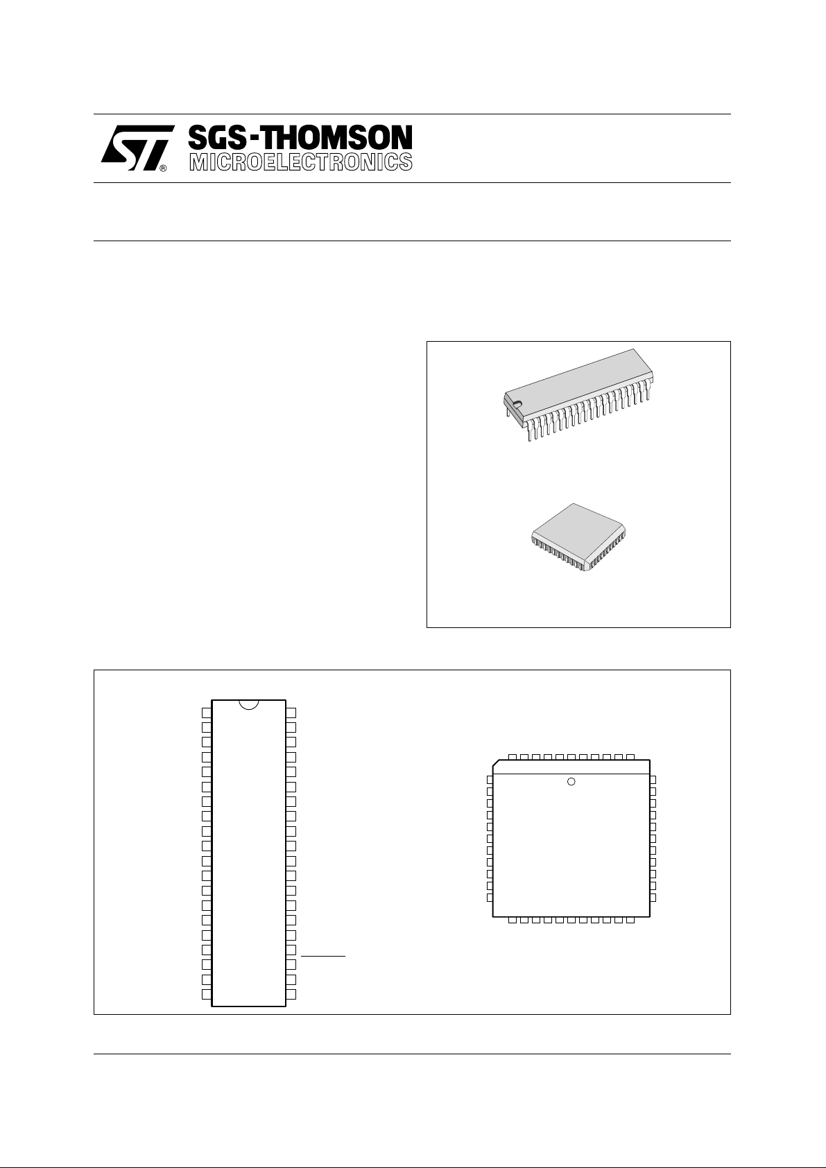
The M5450 and M5451 are monolithic MOS integrated circuits produced with an N-channel silicon
gate technology. They are available in 40-pin dual
in-line plastic packages.
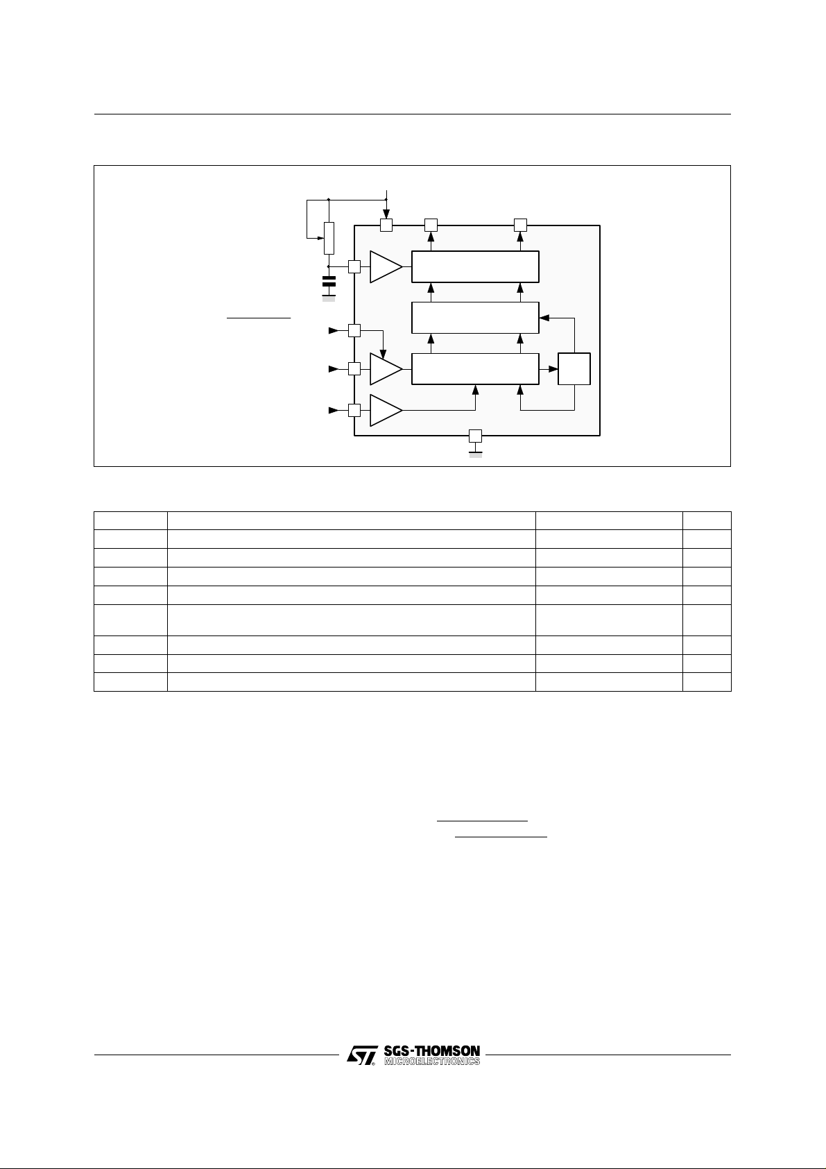
PIN CONNECTION
DIP40
1
V
OUTPUT BIT 17
OUTPUT BIT 16
OUTPUT BIT 15
OUTPUT BIT 14
OUTPUT BIT 13
OUTPUT BIT 12
OUTPUT BIT 11
OUTPUT BIT 10
OUTPUT BIT 9
OUTPUT BIT 8
OUTPUT BIT 7
OUTPUT BIT 6
OUTPUT BIT 5
OUTPUT BIT 4
OUTPUT BIT 3
OUTPUT BIT 2
OUTPUT BIT 1
BRIGHTNESS CONTROL
SS
2
3
4
5
6
7
8
9
10
11
12
13
14
15
16
17
18
19
20
DD
40
OUTPUT BIT 18
39
OUTPUT BIT 19
38
OUTPUT BIT 20
37
OUTPUT BIT 21
36
OUTPUT BIT 22
35
OUTPUT BIT 23
34
OUTPUT BIT 24
33
OUTPUT BIT 25
32
OUTPUT BIT 26
31
OUTPUT BIT 27
30
OUTPUT BIT 28
29
OUTPUT BIT 29
28
OUTPUT BIT 30
27
OUTPUT BIT 31
26
OUTPUT BIT 32
25
OUTPUT BIT 33
24
OUTPUT BIT 34
DATA ENABLE FOR M5450
23
OUTPUT BIT 35 FOR M5451
22
DATA IN
21
CLOCK INV
OUTPUT BIT 13
OUTPUT BIT 12
OUTPUT BIT 11
OUTPUT BIT 10
OUTPUT BIT 9
N.C.
OUTPUT BIT 8
OUTPUT BIT 7
OUTPUT BIT 6
OUTPUT BIT 5
OUTPUT BIT 4
DIP40
(Plastic Package)
ORDER CODE : M5450B7 / M5451B7
PLCC44
(Plastic Chip Carrier)
ORDER CODE : M5451Q
PLCC44
SS
V
OUTPUT BIT 14
OUTPUT BIT 15
6
7
8
9
10
11
12
13
14
15
16
17 29
18
192021222324252627
OUTPUT BIT 3
OUTPUT BIT 2
N.C.
OUTPUT BIT 16
OUTPUT BIT 17
OUTPUT BIT 18
OUTPUT BIT 19
OUTPUT BIT 20
OUTPUT BIT 21
OUTPUT BIT 22
12345
44
DD
V
N.C.
CLOCK IN
OUTPUT BIT 1
BRIGHTNESS CONTROL
40
41
42
43
DATA IN
OUTPUT BIT 35
OUTPUT BIT 34
39
38
37
36
35
34
33
32
31
30
28
OUTPUT BIT 33
OUTPUT BIT 23
OUTPUT BIT 24
OUTPUT BIT 25
OUTPUT BIT 26
OUTPUT BIT 27
N.C.
OUTPUT BIT 28
OUTPUT BIT 29
OUTPUT BIT 30
OUTPUT BIT 31
OUTPUT BIT 32
5450-01.EPS - 5450-02. EPS
September 1993
1/8
Page 2
M5450 - M5451
BLOCK DIAGRAM (Figure 1)
BRIGTHNESS
CONTROL
100kΩ
19
V
DD
OUTPUT
BIT 34
20 24
OUTPUT
BIT 1
18
35 OUTPUT BUFFERS
LOAD
RESET
DATA ENABLE (M5450)
OUTPUT35 (M5451)
SERIAL
DATA
CLOCK
23
22
21
35 LATCHES
35-BIT SHIFT REGISTER
1
ABSOLUTE MAXIMUM RATINGS
Symbol Parameter Value Unit
V
DD
V
V
O(off)
I
O
P
tot
T
T
op
T
stg
Stresses above those listed under "Absolute Maximum Ratings" may causes permanent damage to the device. This is a stress rating only and
functional operation of the device at these or any other conditions above those indicated in the operational sections of this specif ic ation is not
implied. Exposure to absolute maximum rating conditions for extended periods may affect device reliability.
Supply Voltage – 0.3 to 15 V
Input Voltage – 0.3 to 15 V
I
Off State Output Voltage 15 V
Output Sink Current 40 mA
Total Package Power Dissipation at 25°C
at 85°C
Junction Temperature 150 °C
j
1
560
Operating Temperature Range – 25 to 85 °C
Storage Temperature Range – 65 to 150 °C
W
mW
5450-03.EPS
5450-01.TBL
FUNCTIONAL DESCRIPTION
Both the M5450 and the M5451 are specially designed to operate 4 or 5-digit alphanumeric displays
with minimal interf ace with the display and the data
source. Serial data transf er from the dat a source to
the display driver is accomplished with 2 signals,
serial data and clock. Using a format of a leading
"1" followe d by the 35 data bits allows data transfer
without an additional load signal. The 35 data bits
are latched after the 36th bit is complete, thus
providing non-multiplexed, direct drive to the display.
Outputs change only if the serial data bits differ
from the previous time.
Display brightness is determined by control of the
output current LED displays.
2/8
A 1nF capacitor should be connec ted to brightness
control, pin 19, to prevent possible oscillations.
A block diagram is shown in figure 1. For the M5450
a
DA T A EN ABLE is used inst ead of the 35th output.
The
DATA ENABLE input is a metal option for the
M5450.
The output current is typically 20 times greater than
the current into pin 19, which is set by an external
variable resistor . There is an internal lim iting r esistor of 400Ω nominal value.
Figure 2 shows the input data format. A start bit of
logical "1" precedes the 35 bits of data. At the 36th
clock a LOAD signal is generated synchronously
with the high state of the clock, which loads t he 35
bits of the shift registers into the latches.
Page 3
M5450 - M5451
At the low state of the clock a RESET signal is
generated which clears all the shift regist ers for the
next set of data. The s hift registers are static master-slave configurations. There is no clear for the
master portion of the first shift register, t hus allowing continuous operation.
There must be a complete set of 36 clocks or the
shift registers will not clear.
When power is first applied to the chip an internal
power ON reset signal is generated which resets
all registers and all latches. The START bit and the
first clock return the chip to its normal operation.
Bit 1 is the first bit following the start bit and it will
appear on Pin 18. A logical "1" at the input will turn
on the appropriate LED.
Figure 3 shows the timing relationship between
Data, Clock and
DATA ENABLE.
A max clock frequency of 0.5MHz is assumed.
For applications where a lesser number of output s
are used, it is possible t o either increase the current
per output or operate the part at higher than 1V
V
.
OUT
The following equation can be used for calculations.
T
= [(V
j
(124°C/W) + T
OUT
) (I
) (No. of segments) + (VDD ⋅ 7mA) ]
LED
amb
where :
T
= junction temperature (150°C max)
j
V
= the voltage at the LED driver outputs
OUT
I
= the LED current
LED
124°C/W = thermal coefficient of the package
T
= ambient temperature
amb
The above equation was used to plot Figures 4, 5
and 6.
ST ATIC ELECTRICAL CHARACT ERIST IC S
(T
within operating range, VDD = 4.75V to 13.2V, VSS = 0V , unless otherwise specified)
amb
Symbol Parameter Test Conditions Min. Typ. Max. Unit
V
I
V
V
O(off)
f
clock
Notes : 1. Output matchin g is calculated as the percent variation from I
Supply Voltage 4.75 13.2 V
DD
Supply Current VDD = 13.2V 7 mA
DD
Input Voltage Logical "0" Level
V
I
I
Brightness Input Current (note 2) 0 0.75 mA
B
Brightness Input Voltage (pin 19) Input Current = 750µA,
B
Off State Out. Voltage 13.2 V
Out. Sink Current (note 3)
I
O
Input Clock Frequency 0 0.5 MHz
Output Matching (note 1) ± 20 %
I
O
2. With a fixed resistor on the brightness input some variation in brightness will occur from one device to another.
3. Absolute maximum for each output should be limited to 40mA.
4. The V
voltage should be regulated by the user. See figures 5 and 6 for allowable VO versus IO operation.
O
Logical "1" Level
Segment OFF
Segment ON
± 10µA Input Bias
4.75 ≤ VDD ≤ 5.25
VDD > 5.25
T
= 25oC
amb
VO = 3V
VO = 1V (note 4)
Brightness In. = 0µA
Brightness In. = 100µA
Brightness In. = 750µA
+ I
MAX
MIN
/2.
- 0.3
2.2
VDD - 2
3 4.3 V
0
2
12
2.7
15
0.8
V
V
DD
DD
10
10
4
25
V
V
V
µA
µA
mA
mA
5450-02.TBL
3/8
Page 4

M5450 - M5451
Figure 2 : Input Data Format
CLOCK
DATA
LOAD
(INTERNAL)
RESET
(INTERNAL)
Figure 3
CLOCK
DATA
DATA ENABLE
1
START
BIT 1
300ns (min.)
100ns (min.)
Figure 4
P (W)
tot
1.0
0.8
0.6
0.4
0.2
36
BIT 34 BIT 35
SAFE OPERATING
AREA
15mA/segment
34 segments
V = 1V
O
T
(˚C)
amb
5450-04.EPS
Figure 5
V (V)
O
3.2
2.8
2.4
2.0
1.6
1.2
0.8
T
amb
0.4
T = 150˚C (max.)
j
4
= 85˚C
8121620240
20 segments
30 segments
34 segments
I (mA)
LED
28 32
0
5450-05.EPS
Figure 6
105
5450-07.EPS
85
65
45
25
5
0
I (mA)
0
48
20 40 60 80 100
T = 85˚C
amb
V
V
V
I
= 1V
O
= 1.5V
O
= 2V
O
O (max.)
= 40mA
N˚ Segm.
12 16
20 24 28 32
36
40
5450-06.EPS
5450-08.EPS
4/8
Page 5

TYPICAL APPL ICA T IONS
BASIC ELECT RO NICAL LY TUNED RADIO O R TV SY STE M
AM
FM
34 SEGMENTS
M5450
DISPLAY
DRIVER
M5450 - M5451
KEYBOARD
DUPLEXING 8 DIGITS WITH O NE M5450
V
DD
V
LED
.
.
9 16 28 40 32 39 24 31
ELECTRONIC
TUNING
CONTROLLER
STATION
DETEC. ETC.
.
....
PLL
SYNTHESIZER
V
LED
.
5450-09.EPS
V
DD
CLOCK IN
DATA IN
211822
BRIGHTNESS
CONTROL
M5450
19
20
1 23
V
DD
17
5450-10.EPS
5/8
Page 6

+V
C
V
OUT+VD
M5450 - M5451
POWER DISSIPATION OF THE IC
The power dissipation of the IC c an be limited using
different configurations .
a) In the application R must be chosen taking into
account the worst operating conditions.
+V
a)
V
OUT
C
R
I
D
V
D
R is determined by the maximum number of segments activated
V
R =
C
− V
D MAX
N
MAX
− V
⋅ I
O MIN
D
The worst case condition for the device is when
roughly half of the maximum number of segments
are activated.
It must be checked that the total power diss ipation
does not exceed the absolute maximum ratings of
the device.
In critical cases more resistors can be used in
conjunction with groups of segments.
In this case the current variation in the single
resistor is reduced and P
limited.
tot
b) In this configuration the drop on the serial con-
nected diodes is quite stable if the diodes are
properly chosen.
The total power dissipation of the I C depends, in a
first approximation, only on the number of segments activated.
+V
b)
c) In this configuration V
5450-11.EPS
C
+ VD is constant. The
OUT
total power dissipation of the IC depends only on
the number of segments activated.
c)
5450-12.EPS
5450-13.EPS
6/8
Page 7

PACKA G E MECHANICAL DAT A
40 PINS - PLASTIC DIP
M5450 - M5451
a1
I
L
b
b2
e
E
e3
D
40
21
F
120
Dimensions
a1 0.63 0.025
b 0.45 0.018
b1 0.23 0.31 0.009 0.012
b2 1.27 0.050
D 52.58 2.070
E 15.2 16.68 0.598 0.657
e 2.54 0.100
e3 48.26 1.900
F 14.1 0.555
i 4.445 0.175
L 3.3 0.130
Min. Typ. Max. Min. Typ. Max.
Millimeters Inches
b1
PM-DIP40.EPS
DIP40.TBL
7/8
Page 8

M5450 - M5451
PACKA G E MECHANICAL DAT A
44 PINS - P LASTIC CHIP CARRIER
C
M1
M1
B
6
7
21
3944
38
FeF1
e3
E
17
18
29
28
M
M
d2
Dimensions
A
G
(Seating Plane Coplanarity)
Millimeters Inches
Min. Typ. Max. Min. Typ. Max.
d1
D
A 17.4 17.65 0.685 0.695
B 16.51 16.65 0.650 0.656
C 3.65 3.7 0.144 0.146
D 4.2 4.57 0.165 0.180
d1 2.59 2.74 0.102 0.108
d2 0.68 0.027
E 14.99 16 0.590 0.630
e 1.27 0.050
e3 12.7 0.500
F 0.46 0.018
F1 0.71 0.028
G 0.101 0.004
M 1.16 0.046
M1 1.14 0.045
PMPLCC44.EPS
PLCC44.TBL
Information furnished i s believed to be accurate and rel iabl e. However, S GS-THOMSON Microel ectroni cs assumes no responsibil ity
for the consequences of use of such information nor for any infringement of patents or other rights of third parties which may result
from its use. No licence is granted by implication or otherwise under any patent or patent rights of SGS-THOMSON Microelectronics.
Specifications mentioned in this publication are subject to change without notice. This publication supersedes and replaces all
information previously supplied. SGS-THOMSON Microelectronics products are not authorized for use as critical components in life
support devices or systems without express written approval of SGS-THOMSON Microelectronics.
© 1994 SGS-THOMSON Microelectronics - All Rights Reserved
2
Purchase of I
2
C Patent. Rights to use these components in a I2C system, is granted provided that the system conforms to
I
Australia - Brazil - China - France - Germany - Hong Kong - Italy - Japan - Korea - Malaysia - Malta - Morocco
The Netherlands - Singapore - Spain - Sweden - Switzerland - Taiwan - Thailand - United Kingdom - U.S.A.
C Components of SGS-THOMSON Microelectronics, conveys a license under the Philips
2
C Standard Specifications as defined by Philips.
the I
SGS-THOMSON Microelectronics GROUP OF COMPANIES
8/8
 Loading...