

Page 1
Outline 16P2E-A
16
13
14
15
1
4
3
2
12
5
11
6
7
8
10
9
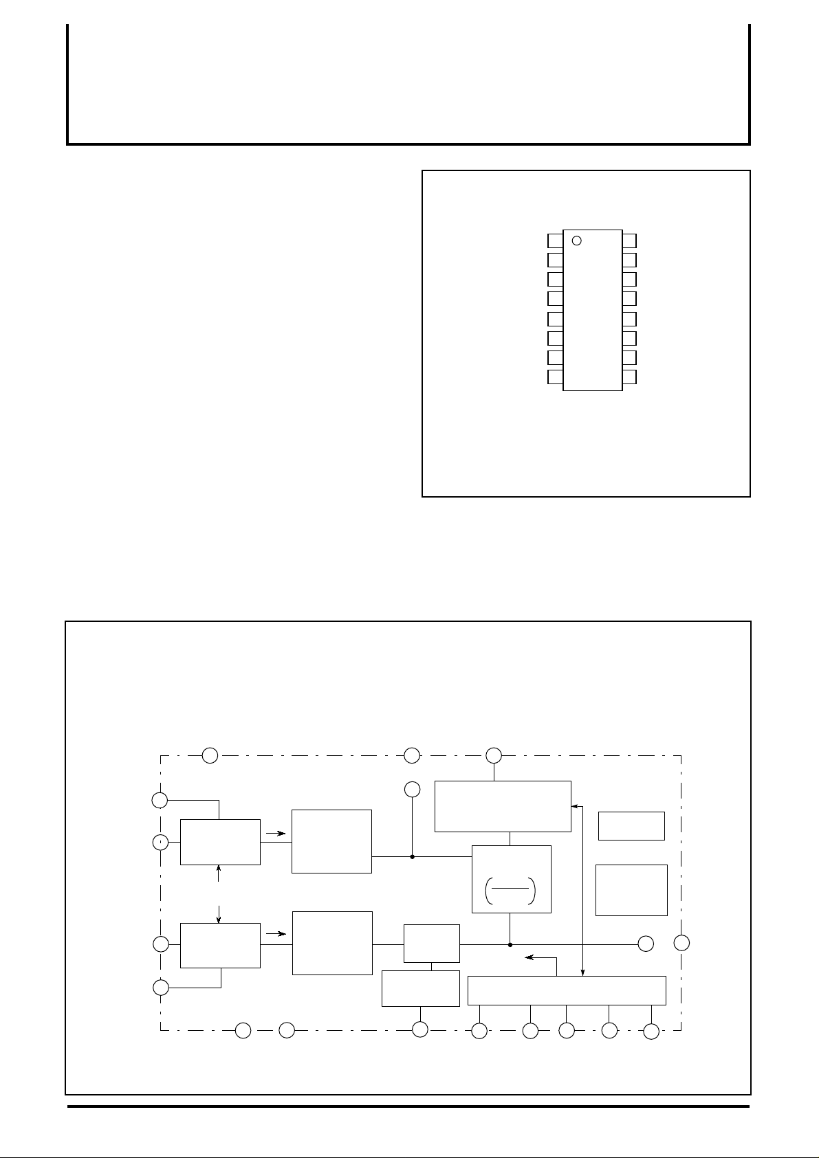
M52957FP
PSDN
CHN
V
CC
(TESTN)
NC
STB
CINT
RESET
SOUT
PSDF
CHF
GND1
(TESTF)
NC
GND2
CLALV
HOLD
INT
MITSUBISHI ICs (AV COMMON)
M52957FP
DISTANCE DETECTION SIGNAL PROCESSING FOR 3V SUPPLY VOLTAGE
DESCRIPTION
M52957FP is a semiconductor integrated circuit containing
distance detection signal processing circuit for 3V supply voltage.
This device transforms each optical inflow current I1 and I2 from
PSD SENSOR into the voltage, and integrates that output after
doing calculation corresponds to I1/(I1+I2), and outputs it as the
time data(pulse term).
FEATURES
Wide supply voltage range Vcc=2.2 to 5.5V
•
Includes clamp level switching circuit
•
(Switch is 16 kinds by outside control)
Includes standby function
•
Includes power on RESET function
•
APPLICATION
Auto focus control for the CAMERA
Sensor for short distance etc
RECOMMENDED OPERATING CONDITION
Supply voltage range......................................................2.2 to 5.5V
Rated supply voltage.................................................................3.0V
PIN CONFIGURATION
(TOP VIEW)
NC:NO CONNECTION
BLOCK DIAGRAM
CHN
2
1
PSDN
PSDF
CHF
16
15
VCC
3 4
TESTN
1
STATIONARY
LIGHT
REMOVE
HOLD
HOLD
STATIONARY
LIGHT
REMOVE
14
GND1
I
I2
12
GND2
I/V
TRANSFORM
AMP
I/V
TRANSFORM
AMP
Note: pin4,13 is connected only engineering sample
NC
CLANP
CIRCUIT
CLAMP LEVEL
SWITCHING
11
CLALV STB RESET INT HOLD SOUT
CINT
6
PULSE WIDTH
TRANSFORM
(DOUBLE INTEGRATION)
RECKON
I1
I1+I2
HOLD
SEQUENTIAL CONTROL LOGIC
5
7
9
BIAS
REFERENCE
VOLTAGE
10
TESTF
13
NC
8
1
Page 2
≥
±
MITSUBISHI ICs (AV COMMON)
M52957FP
DISTANCE DETECTION SIGNAL PROCESSING FOR 3V SUPPLY VOLTAGE
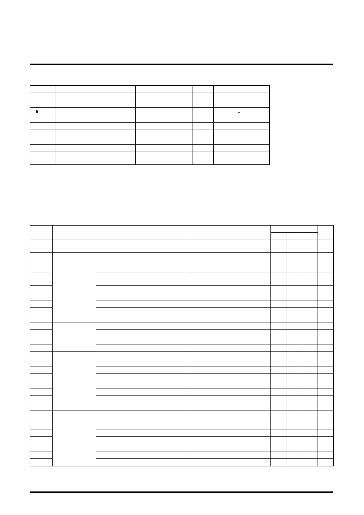
ABSOLUTE MAXIMUM RATINGS
(Ta=25˚C,unless otherwise noted)
Symbol Parameter Ratings Unit Remark
V
CC
Supply voltage 7.0 V note 1
Pd Power dissipation 320 mW Ta=25˚C
K
V
IF
V
I/O
I
sout
T
opr
T
stg
surge
V
Note 1. As a principle,do not provide a supply voltage reversely.
2. As a principle,do not provide the terminals with the voltage over supply voltage or under ground voltage.
ELECTRICAL CHARACTERISTICS
Thermal derating -3.2 mW/ ˚C
Ta 25˚C
Pin supply voltage 7.0 V Pin5,7,8,9,10,11
Another pin supply voltage -0.3 to V
+0.3 V note 2
CC
Output pin inflow current 0.5 mA NPN open collector
Operating temperature -10 to 50 ˚C
Storage temperature -40 to 125 ˚C
Surge voltage
200V over
C=200PF
R=0 Ω
(Ta=25˚C,Vcc=3.0V, unless otherwise noted)
Symbol Classification Parameter Test conditions
CC
V
CC1
I
CC2
I
CC3
I
CC4
I
V
HOH
V
HOL
I
HOH
I
HOL
V
INH
V
INL
I
INH
I
INL
V
CLH
V
CLL
I
CLH
I
CLL
V
REH
V
REL
I
REH
I
REL
V
STH
STL
V
STH
I
STL
I
CHQC
I
CHC
I
CHD
I
Consuming
current
HOLD pin
INT pin
CLALV pin
RESET pin
STB pin
HOLD C
Operating supply
voltage range
Usual consuming current - 5.9 7.7 mA
While Rapid charge
consuming current 1
While Rapid charge
consuming current 2
While CH rapid charge
consuming current
While CH and CINT rapid charge
consuming current
While STAND BY consuming current - - 1.0 µ A
HOLD "H" input voltage 1.1 - 7.0 V
HOLD "L" input voltage -0.3 - 0.3 V
HOLD "H" input current V
HOLD "L" input current V
=5.5V - - 1.0 µ A
IH
=0V -100 -75 -50 µ A
IL
INT "H" input voltage 1.1 - 7.0 V
INT "L" input voltage -0.3 - 0.3
INT "H" input current V
INT "L" input current V
=5.5V - - 1.0 µ A
IH
=0V -100 -75 -50 µ A
IL
CLALV "H" input voltage 1.1 - 7.0 V
CLALV "L" input voltage -0.3 - 0.3 V
CLALV "H" input current V
CLALV "L" input current V
=5.5V - - 1.0 µ A
IH
=0V -100 -75 -50 µ A
IL
RESET "H" input voltage 1.1 - 7.0 V
RESET "L" input voltage -0.3 - 0.3
RESET "H" input current V
RESET "L" input current V
=5.5V - - 1.0 µ A
IH
=0V -100 -75 -50 µ A
IL
STB "H" input voltage
STB "L" input voltage -0.3 - 0.3 V
STB "H" input current V
STB "L" input current V
CH rapid charge current IPSD=5 µ A,
CH stationary charge current
CH stationary discharge current V
IH
=5.5V - - 3.0 µ A
IL
=0V -150 -100 -50 µ A
CH
V
=0V -2000 -1000 -500 µ A
CH
V
=0V -30 -20 -10 µ A
CH
=1.5V 10 20 30 µ A
Limits
Min. Typ. Max.
2.2 3.0 5.5 V
- 17.7 23.0 mA
- 19.0 24.7 mA
V
CC
-0.3
- 7.0 V
Unit
V
V
2
Page 3
∆
µ
MITSUBISHI ICs (AV COMMON)
M52957FP
DISTANCE DETECTION SIGNAL PROCESSING FOR 3V SUPPLY VOLTAGE
∆
∆
∆
∆
∆
∆
∆
∆
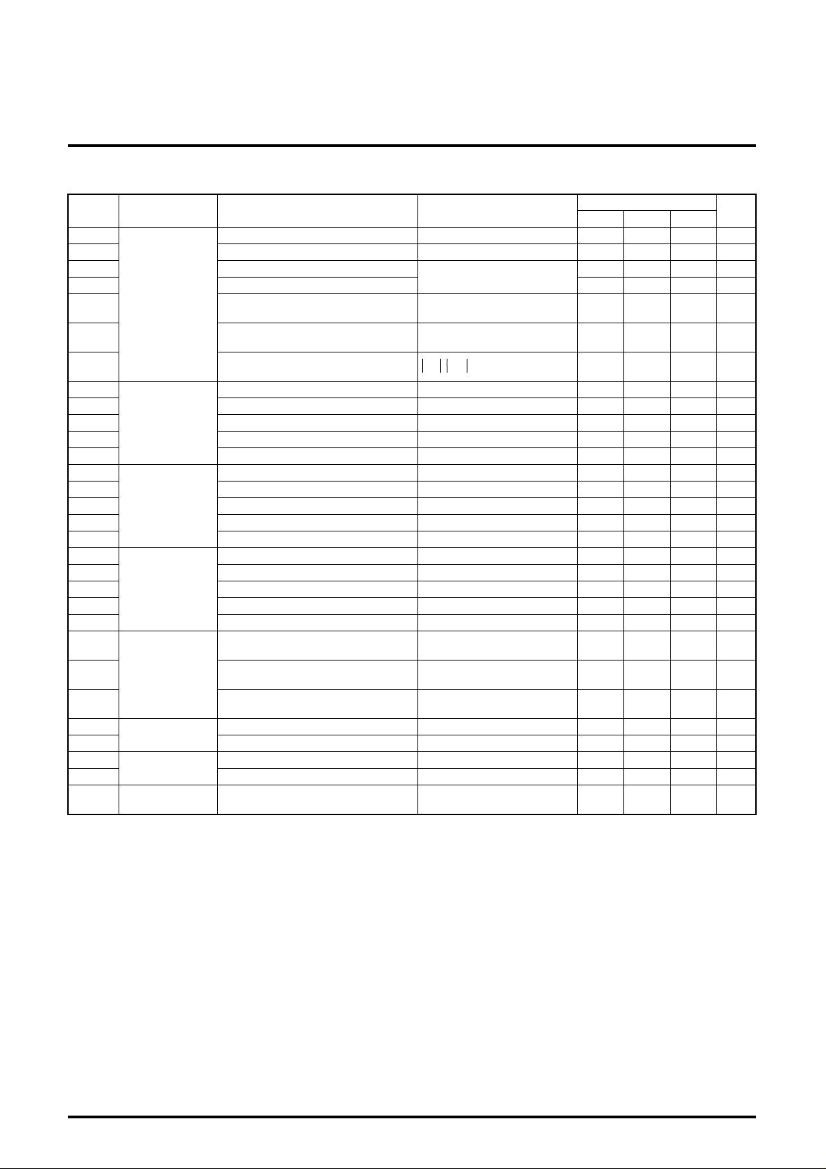
ELECTRICAL CHARACTERISTICS
Symbol Classification Parameter Test conditions
I
CINTC
V
CINT
I
CI1
CI2
I
∆
I
CI1
I
CI2
∆
CI12
I
(9:1)-1
D
D
(6:4)-1
(3:7)-1
D
AF-1 AF slope -1 6.57 8.89 11.21 msec
Double
integration
AF input
condition 1
CINT rapid charge current V
CINT reference voltage GND criterion 1.6 1.8 2.0 V
The first integration current
The second integration current -3.31 -2.54 -1.77 µ A
The first integration
current stability percentage
The second integration
current stability percentage
The first and second
integration current ratio
AF output time(9:1)-1 Near side 9 : Far side 1 11.78 13.40 15.02 msec
AF output time(6:4)-1 Near side 6 : Far side 4 7.77 8.95 10.13 msec
AF output time(3:7)-1 Near side 3 : Far side 7 3.77 4.51 5.25 msec
(cont.)
Limits
Min. Typ. Max.
=1V(CINT stable period) 84 120 156 µ A
CI
V
V
I
CI1
CINT
CHF
=1.5V
=2V, V
/ I
CI2
CHN
=0V
4.2 6.0 7.8
- - 10 %
- - 10 %
2.12 2.36 2.60
LAF-1 AF linearity-1 0.9 1.0 1.1
(9:1)-2
D
D
(6:4)-2
(3:7)-2
D
AF-2 AF slope -2 6.57 8.89 11.21 msec
AF input
condition 2
AF output time(9:1)-2 Near side 9 : Far side1 11.78 13.40 15.02 msec
AF output time(6:4)-2 Near side 6 : Far side4 7.77 8.95 10.13 msec
AF output time(3:7)-2 Near side 3 : Far side7 3.77 4.51 5.25 msec
LAF-2 AF linearity-2 0.9 1.0 1.1
(9:1)-3
D
D
(6:4)-3
(3:7)-3
D
AF-3 AF slope -3 6.57 8.89 11.21 msec
AF input
condition 3
AF output time(9:1)-3 Near side 9 : Far side1 11.78 13.40 15.02 msec
AF output time(6:4)-3 Near side 6 : Far side 4 7.77 8.95 10.13 msec
AF output time(3:7)-3 Near side 3 : Far side 7 3.77 4.51 5.25 msec
LAF-3 AF linearity-3 0.9 1.0 1.1
D
(9:1)
AF output time(9:1)
AF input
condition
(6:4)
D
AF output time(6:4)
1 minus 2
(3:7)
D
SOUTL
I
VSOUTS SOUT saturation voltage IOUT=500µA - - 0.3 V
∆INF
IPSD Stationary light remove current - - 30 µA
CLAM
I
Data
Sensor
AF output time(3:7)
SOUT leak current V
Signal light saturation current 3.0 - - µA
Clamp level Change quantity for Typ.
Near side 9 : Far side1
(Consition 1-2)
Near side 6 : Far side4
(Consition 1-2)
Near side 3 : Far side7
(Consition 1-2)
IN
=5.5V - - 1.0 µA
current
- - 280 µ sec
- - 280 µ sec
- - 280 µ sec
-30 - 30 %
Unit
A
3
Page 4

MITSUBISHI ICs (AV COMMON)
M52957FP
DISTANCE DETECTION SIGNAL PROCESSING FOR 3V SUPPLY VOLTAGE
ICC2, ICC3, ICC4, ICHQC, ICHC, ICHD, ICINTC, VCINT, ICI1, ICI2
Set up the logic control terminal, correspond to the parameter.
∆ICI1, ∆ICI2
Change ratio between the first integration current and the second
integration current at a voltage of CINT that is
{CINT reference voltage(VCINT) to 0.1V} and 1V.
CI1=(1- ) X 100%
∆I
CI2=(1- ) X 100%
∆I
D
(9 :1)-1, D(6 : 4)-1, D(3 : 7)-1, ∆AF-1, LAF-1, D(9 :1)-2, D(6 : 4)-2,
The first integration current (CINT=1V)
The first integration current (C
The second integration current (C
The second integration current (C
INT=VCINT to 0.1V)
INT=1V)
INT=VCINT to 0.1V)
D(3 : 7)-2, ∆AF-2, LAF-2, D(9 :1)-3, D(6 : 4)-3, D(3 : 7)-3, ∆AF-3, LAF-3
Connect the resistance of 120kΩ instead of PSD and establish
current output from photo coupler correspond to the parameter. And
input the varied resistance ratio. And measure the pulse width of
APPLICATION EXAMPLE
OUT output at that time,obtain AF slope and AF linearity from the
S
equations below.
Input condition1 : IPSD(Stationary light current)=0 I1+I2=100nA
Input condition2 : IPSD(Stationary light current)=0 I1+I2=50nA
Input condition3 : IPSD(Stationary light current)=10 µA I1+I2=100nA
(9 : 1)....The pulse width of SOUT output at input with I1:I2=9:1
D
D(6 : 4)....The pulse width of SOUT output at input with I1:I2=6:4
D(3 : 7)....The pulse width of SOUT output at input with I1:I2=3:7
AF slope : ∆AF=D(9 : 1) - D(3 : 7)
AF linearity : L(AF)=(D(9 : 1) - D(6 : 4))/(D(6 : 4) - D(3 : 7))
PSD quite resistance : 120kΩ
∆INF, IPSD
The input current of one side channel when stationary light remove
circuit and I/V transform AMP is not saturated.
1.0µF
PSD
1.0µF
CHN
PSDN
PSDF
CHF
2
1
16
15
V
CC
3
STATIONARY
LIGHT
REMOVE
HOLD
HOLD
STATIONARY
LIGHT
REMOVE
14 12 11 5 7 9 10
11
I/V
TRANSFORM
AMP
12
I/V
TRANSFORM
AMP
GND2GND1
0.056µF
4 6
TESTN
CLAMP LEVEL
SWITCHING
CLALV STB RESET INT HOLD SOUT
CINTNC
PULSE WIDTH
TRANSFORM
(DOUBLE INTEGRATION)
RECKON
I1
I1+I2
CLAMP
CIRCUIT
HOLD TESTF
SEQUENTIAL CONTROL LOGIC
MICROCOMPUTER
REFERENCE
VOLTAGE
BIAS
NC
13
CC
PV
8
IRED
4
Page 5

MITSUBISHI ICs (AV COMMON)
M52957FP
DISTANCE DETECTION SIGNAL PROCESSING FOR 3V SUPPLY VOLTAGE
CONTROLS
(1) STB
This terminal enables IC to operate. IC is Standby at HIGH in
this terminal. IC can operate at LOW in this terminal.
(2) RESET
This terminal resets the whole IC including a logic. This terminal
resets IC at HIGH. This terminal cancel resetting IC at the edge
from HIGH to LOW. IC includes power on reset function. The
control from external is also possible. The reset term in IC
takes OR between power on reset and control signal from
external.
H
L
Indefiniteness Reset Reset canceled
While this terminal is HIGH,dielectric divide pole
countermeasures circuit of integration condenser is active.
(3) CLALV
This terminal sets up clamp level.
As including D/A of 4bit,16way clamp level setting is possible by
inputting clock after reset is canceled(include none clamp).
Set up current value of each bit is on the right table.
The number of input clock and set up clamp level is as follows.
Bit Set up current (Typ.)
1 0.125 nA
2 o.25 nA
3 0.5 nA
4 1.0 nA
Clock
value
0 None clamp 12 1.500 nA
1 0.125 nA 13 1.625 nA
2 0.250 nA 14 1.750 nA
3 0.375 nA 15 1.875 nA
4 0.500 nA 16 None clamp
5 0.625 nA 17 0.125 nA
6 0.750 nA 18 0.250 nA
7 0.875 nA 19 0.375 nA
8 1.000 nA 20 0.500 nA
9 1.125 nA
10 1.250 nA
11 1.375 nA
Clamp
level(Typ.)
Clock
value
Clamp
level(Typ.)
Clamp level is established with fall edge of input clock.
It repeats the same value after 16 clock.
5
Page 6

DISTANCE DETECTION SIGNAL PROCESSING FOR 3V SUPPLY VOLTAGE
(4) HOLD, INT
These terminals implement the following controls by inputting
HIGH/LOW.
a. CINT rapid charge ON, OFF
b. CH rapid charge ON, OFF
c. Stationary light hold ON, OFF
d. The first integration ON, OFF
e. The second integration ON, OFF
HOLD
MITSUBISHI ICs (AV COMMON)
M52957FP
Stationary light hold
INT
C
rapid charge
INT
Reset canceled
CH
rapid charge
a. CINT rapid charge
After reset is canceled, the capacity of CINT is charged rapidly
until INT terminal first falls.
b. CH rapid charge
After reset is canceled, the capacity of CH is charged rapidly
until INT terminal first rises and falls.
c. Stationary light hold
After reset is canceled, holds the stationary light while HOLD
terminal is HIGH.
The first
integration
The second
integration
(5) SOUT
When the second integration starts,This terminal becomes from
HIGH to LOW. If CINT terminal exceeds judge level or INT
terminal becomes from HIGH to LOW, this terminal becomes
from LOW to HIGH.
(notice) As the signal from microcomputer,the signal that controls
IRED ON/OFF is required except for above mentioned
control signals. But applying the timing of HOLD is
available.
d. The first integration
After reset is canceled, as HOLD terminal is HIGH and INT
terminal is HIGH, the first integration is implemented while INT
terminal is HIGH. Therefore,the first integration must be
finished(INT terminal from HIGH to LOW) until stationary light
hold will be completed (HOLD terminal from HIGH to LOW)
e. The second integration
After reset is canceled, the second integration is implemented as
HOLD terminal is LOW and INT terminal is HIGH. And,the
second integration is completed by exceeding judgement level of
CINT terminal although INT terminal is HIGH.
6
Page 7

DISTANCE DETECTION SIGNAL PROCESSING FOR 3V SUPPLY VOLTAGE
SEQUENTIAL TIME CHART EXAMPLE
MITSUBISHI ICs (AV COMMON)
M52957FP
The second
integration
1m
sec
16msec
10µsec
µsec
MIN5
50µsec
50µsec
min500uS
555µX128times 71msec
Stationary light hold,the first integrationX128times
Measurement
circuit stable
period
1msec
CH rapid
Reset period
Movement period
ofCINT dielectric
charge period
10µsec
dividepole
measures circuit
25msec
10µsec
100µ
sec
25msec
µsec
100
Input signal
7
(F)
VCC
STB
RESET
CLALV
HOLD
IRED
INT
Output signal
SOUT
IC control content
CINT rapid charge
CH rapid charge
The first integration
Stationary light hold
The second integration
pin
TESTN
CINT pin
Page 8

DISTANCE DETECTION SIGNAL PROCESSING FOR 3V SUPPLY VOLTAGE
1.0nA0.25nA 0.5nA0.125nA
MASK OPTION
(1) The second integration current value can be doubled.
(2.5µ 5.0µA)
(2) Control terminal variation
1
Full spec (typical)
MITSUBISHI ICs (AV COMMON)
M52957FP
C
L
A
L
V
11 5 7 9 10 8
S
T
B
R
E
I
S
N
E
T
T
MICROCOMPUTER
S
H
O
O
U
L
T
D
This type uses CLALV, STB, RESET, INT, HOLD, SOUT terminal as
I/F terminal to the microcomputer.
This is the typical type at M52957FP.
2
Most simplified type
S
H
O
O
I
N
T
9 10 8
MICROCOMPUTER
U
L
T
D
Fixes 3 parts of 4 switches correspond to each bit in figure to ON or
OFF,controls another part by CLALV terminal .
(b) STB
When no standby function required such as V
CC is switched ON/
OFF,STB terminal can be eliminated.
(c) RESET
Since IC include power on reset circuit,RESET terminal can be
eliminated. As merit of controlling RESET terminal from
outside,distance detection time can be shortened because
there is no need to switch VCC or STB Terminal ON /OFF at
consecutive distance detection.
This type does not connect CLALV, STB, RESET terminals to the
microcomputer.
When above mentioned terminals are not connected to the
microcomputer without changing mask,connect each terminal to
the ground. In this case,clamp level becomes 0 and standby
function is lost. Power on reset in IC is used as reset.
3
Explanation of the terminal that can be simplified.
(a) CLALV
In the typical type,16way clamp le v els can be set b y the external
control,but also the terminal can be simplified by mask option
as follows.
1. Clamp level fixation
Selects 1 point from 16 steps of clamp level and fixes it.
2. Clamp level 2 step changeover
Selects 2 points from clamp level and switches it by changing
CLALV terminal HIGH/LOW. However,as selecting 2 points,
there is a following constraint.
8
Page 9

DISTANCE DETECTION SIGNAL PROCESSING FOR 3V SUPPLY VOLTAGE
DESCRIPTION OF PIN
Name Peripheral circuit of pins Parameter
HOLD
INT
CLALV
RESET
"H" input
voltage
"L" input
voltage
"H" input
current
"L" input
current
MITSUBISHI ICs (AV COMMON)
M52957FP
Limits
Min. Typ. Max.
1.1 - 7.0
- - 0.3
- - 1.0
-100 -75 -50 V
Unit
V
µA
Test conditions
and note
V
IH=5.5V
IL=0V
STB
SOUT
"H" input
voltage
"H" input
voltage
"H" input
current
"L" input
current
"L" output
voltage
"H" leak
current
CC
V
-0.3
- - 0.3
- - 3.0
-150 -100 -50 V
- - 0.3 V I
- - 1.0 µAVIN=5.5V
- 7.0
µA
V
IH=5.5V
V
IL=0V
OL=500µA
9
 Loading...