

Page 1
M I T S U B I S H I
- 9
MITSUBISHI ICs (AV COMMON)
M52795SP/FP
AV SWITCH with I2C BUS CONTROL
PRELIMINARY
Some parametric limits are subject to change.
DESCRIPTION
FEATURES
APPLICATION
Video equipment
RECOMMENDED OPERATING CONDITION
(Lead pitch :1.778mm)
PIN CONFIGURATION ( TOP VIEW )
(Lead pitch :1.27mm)
of
output 0dB or 6dB .
123456714131211109
D5
Lch T IN
Rch 1 OUT
TUNER IN
8
DC
Rch 2 IN
VCC
VIDEO 3 IN
VIDEO 4 IN
SDADDSCL
28272625242322151617181920
21
Lch 2 OUT
BIAS
GND
123456714131211109
D4
Lch T IN
Rch 1 OUT
TUNER IN
8
DC
Rch 2 IN
VCC
VIDEO 3 IN
VIDEO 4 IN
SDADDSCL
28272625242322151617181920
21
Lch 2 OUT
BIAS
GND
Notice. This is not a final specification.
The M52795 is AV switch semiconductor integrated circuit with
I2C bus control .
This IC contains 2-channels of 4-input audio switches and 2channels of 4-input video switches. Each channel can be
controled independently .
The video switches contain amplifiers can be controled a gain
•Video and stereo sound switches in one package
•Wide frequency range ( video switch )...........DC~20MHz
•High separation ( video switch )
..................Crosstalk -60dB ( typ. ) at 1MHz
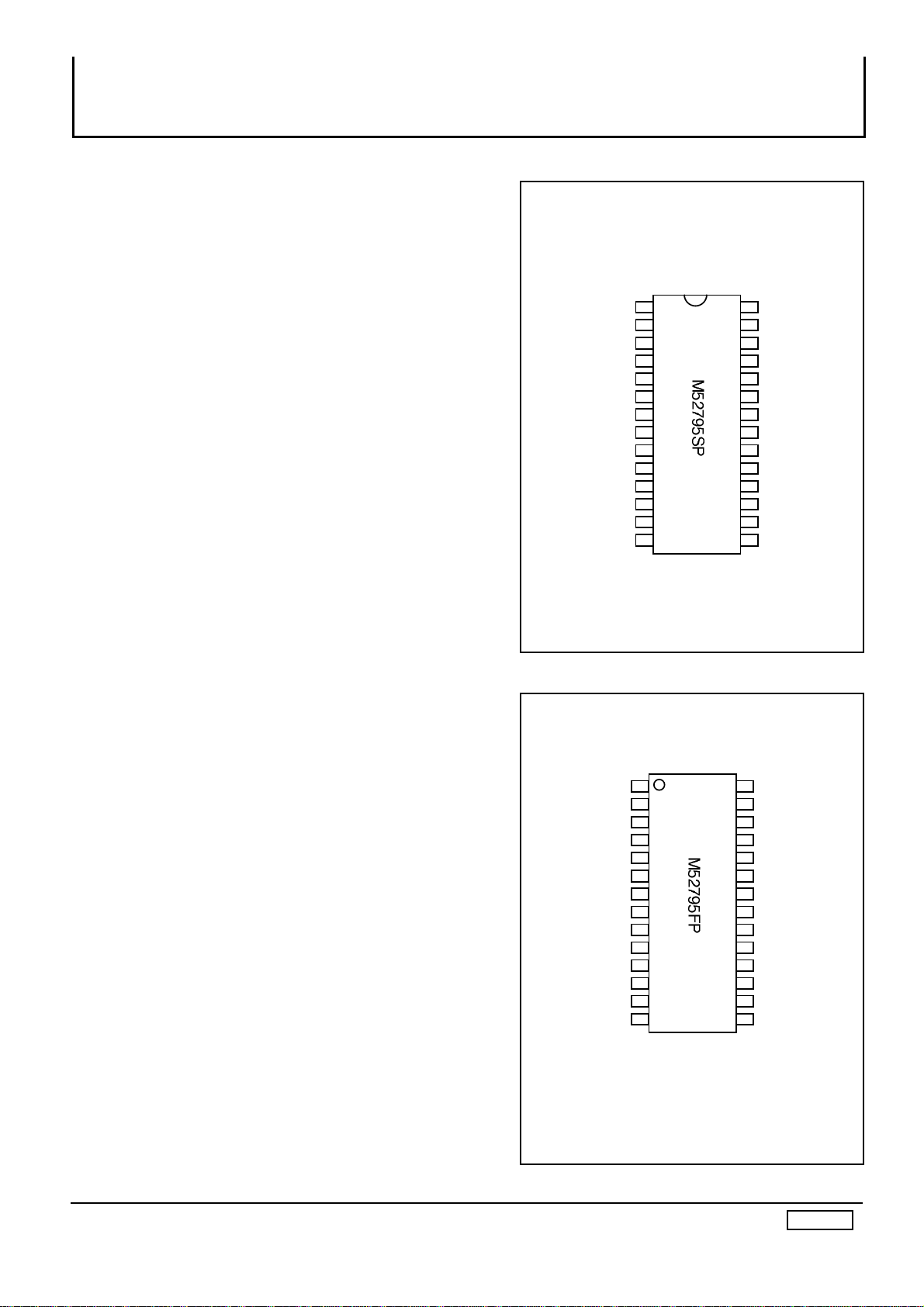
•Two types of packages are provided : SDIP with a lead pitch of
1.778mm ( M52795SP ) ; and SOP with a lead pitch of 1.27mm
( M52795FP ) .
PIN CONFIGURATION ( TOP VIEW )
Lch 2 IN
VIDEO 2 IN
Lch 3 IN
Rch 3 IN
Lch 4 IN
Rch 4 IN
Outline 28P4B
D4
Rch T IN
Lch 1 OUT
V 1 OUT
V 2 OUT
Rch 2 OUT
CHIP SELECT
Supply voltage 4.7V~9.3V
Rated supply voltage 5V,9V
Maximum output current 32mA(at 9V)
Lch 2 IN
VIDEO 2 IN
Lch 3 IN
Rch 3 IN
Lch 4 IN
Rch 4 IN
Outline 28P2W-A
D5
Rch T IN
Lch 1 OUT
V 1 OUT
V 2 OUT
Rch 2 OUT
CHIP SELECT
1
AUG.'98
Page 2
M I T S U B I S H I
- 9
MITSUBISHI ICs (AV COMMON)
M52795SP/FP
AV SWITCH with I2C BUS CONTROL
PRELIMINARY
Some parametric limits are subject to change.
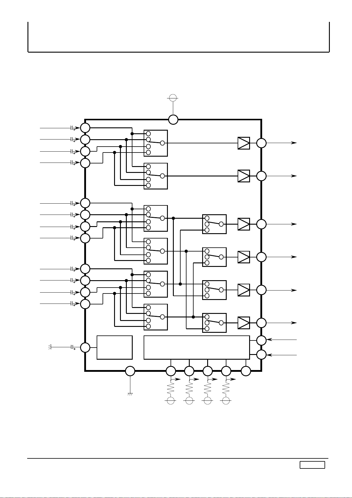
BLOCK DIAGRAM
2
V 2 OUT
I C Control
17
CHIP SELECT
D515D414DDDC7422
Rch 1 OUT
Lch 1 OUT
1921Rch 2 OUT
Lch 2 OUT
LRMRLRLMRLRLMLR
M
Rch T IN
Lch 3 IN
2551127369
Rch 2 IN
Rch 3 IN
Rch 4 IN
Lch 4 IN
Lch 2 IN
Lch T IN
0/6dB
0dB
0dB
0dB
0dB
245781013161820232426
28
V-SW1
V-SW2
R-SW1
R-SW2
L-SW1
L-SW2
R-MODE1
R-MODE2
L-MODE1
L-MODE2
VIDEO 2 IN
TUNER IN
VIDEO 3 IN
VIDEO 4 IN
BIAS
GND
SDA
SCL
Notice. This is not a final specification.
VCC
1
0/6dB
V 1 OUT
BIAS
2
12
AUG.'98
Page 3
M I T S U B I S H I
- 9
MITSUBISHI ICs (AV COMMON)
M52795SP/FP
AV SWITCH with I2C BUS CONTROL
PRELIMINARY
Some parametric limits are subject to change.
234
Lch 3 IN
5
Rch 2 IN
VCC
VIDEO 2 IN
Lch 2 IN
87Rch 3 IN
Lch 4 IN
VIDEO 3 IN
69VIDEO 4 IN
Rch 4 IN
1011SCL12SDA24Rch T IN
25
TUNER IN
26
Lch T IN
3.6V
4.7V
DC14DD27D428D5
30K
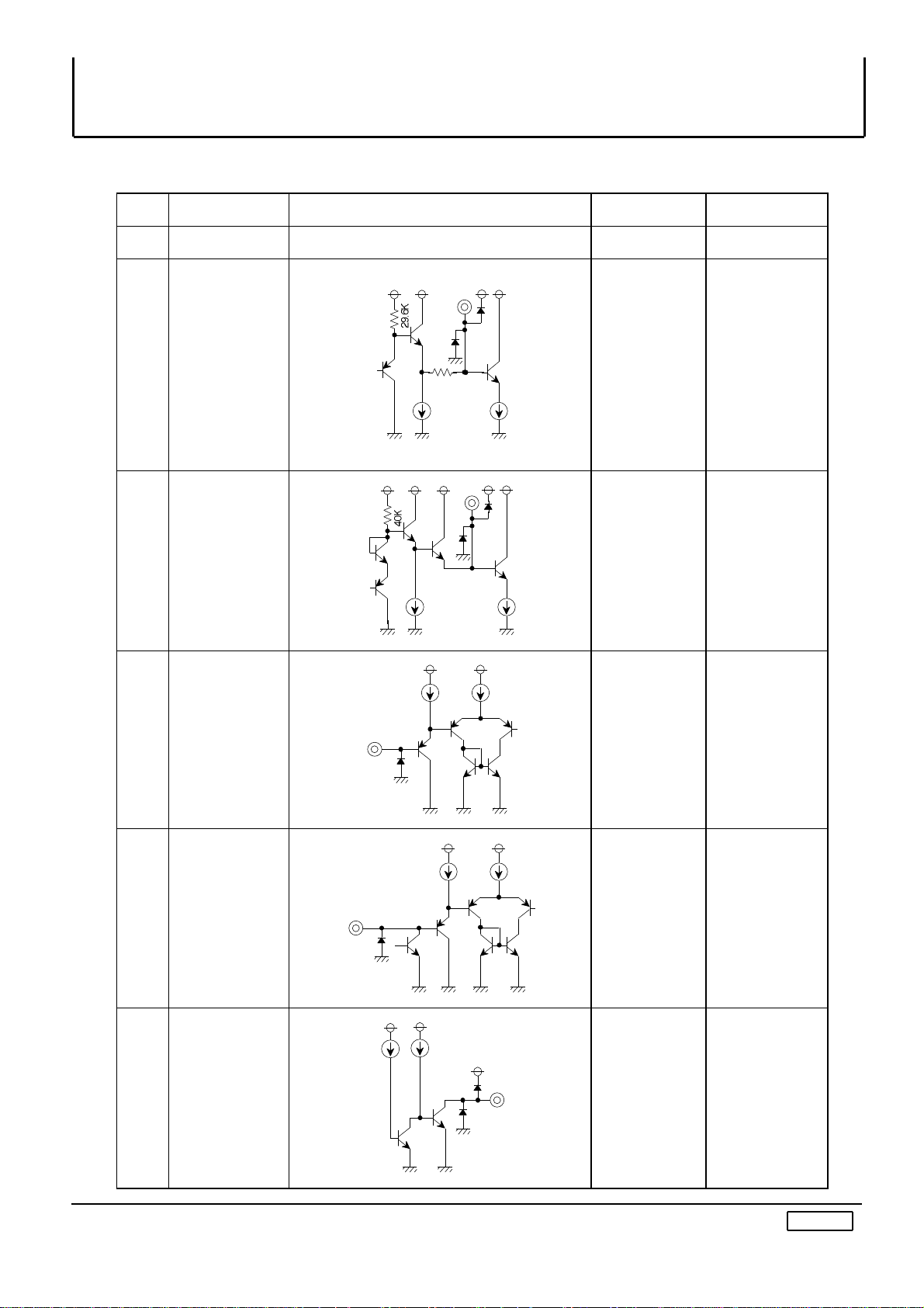
Name
Peripheral circuit pins
DC voltage(V)
Remarks
Notice. This is not a final specification.
DESCRIPTION OF PIN
Pin No.
1
9V
5~9V
Clamp in
VIL max.=1.5V
VIH min.=3.0V
13
VIL max.=1.5V
VIH min.=3.0V
VOL max.=0.4V
(at Iin=3mA)
VOL max.=0.4V
(at Iin=1mA)
3
AUG.'98
Page 4

M I T S U B I S H I
- 9
MITSUBISHI ICs (AV COMMON)
M52795SP/FP
AV SWITCH with I2C BUS CONTROL
PRELIMINARY
Some parametric limits are subject to change.
GND
16
SELECT
17
BIAS
Rch 2 OUT
2021Lch 2 OUT
23
Lch 1 OUT
19
22
V 1 OUT
30K
30K
1.5K
1.5K
15K5K5K
Name
Peripheral circuit pins
Remarks
DC=2.9V
Notice. This is not a final specification.
DESCRIPTION OF PIN (cont.)
Pin No.
15
CHIP
DC voltage(V)
SLAVE
ADDRESS
0~1.5V-------90H
2.5V~Vcc----92H
OPEN--------90H
70K
4.2V
18
Rch 1 OUT
V 2 OUT
4.0V
SYNC CHIP
4
AUG.'98
Page 5

M I T S U B I S H I
- 9
MITSUBISHI ICs (AV COMMON)
M52795SP/FP
AV SWITCH with I2C BUS CONTROL
PRELIMINARY
Some parametric limits are subject to change.
5
A ; Acknownledge
SW2 is controled by DATA2 .
the
wired-AND function .
2
23456789129
A
SDA
MSB
LSB
S
A
DATA2
A
P : Stop
SLAVE ADDRESS
100100X
receiver )
2
Notice. This is not a final specification.
I C BUS
I C BUS(Inter IC BUS)is multi master bus system developed by PHILIPS . Two wires ( SDA - serial data,
SCL - serial clock ) realize functions of start , stop , transferring data , synchronization and arbitration. The
output stages of device connected to the bus must have an open drain or open collector in order to perform
A
LSB
SCL
S
1
S ; Start condition, a high to low transition of the SDA line while SCL is high
P ; Stop condition, a low to high transition of the SDA line while SCL is high
Every byte put on the SDA line must be 8-bits long . Each byte has to be followed by an acknowledge bit. Data
is transferred with the most significant bit (MSB ) first . The data on the SDA line must be stable during the
HIGH period of the clock . The HIGH or LOW state of the data line can only change when the clock signal on
the SCL line is LOW .
MSB
P
CONTROL
This IC controls 2-channel switchs with 2-byte data ( DATA1 and DATA2 ) . SW1 is controled by
DATA1 ,
SLAVE ADDRESS
S : Start
A : Acknowledge
DATA1
0
P
A
R/W bit
Usually ` 0 ` ( W : Master transmitter transmits to slave
Possible to select
16PIN Hi:1,Lo:0
AUG.'98
Page 6

M I T S U B I S H I
- 9
MITSUBISHI ICs (AV COMMON)
M52795SP/FP
AV SWITCH with I2C BUS CONTROL
PRELIMINARY
Some parametric limits are subject to change.
Data byte format
6
M52795 FUNCTION TABLE
S
SLAVE ADDRESS
A
DATA(D7~D0)
A
DATA(DF~D8)
APSLAVE ADDRESS
SLAVE ADDRESS
A6A5A4A3A2A1A0
R/W100100
0 / 10DATA1(D7~D0) CONT
DATA
D7D6D5D4D3D2D1D0CONT
AUDIO MODE
I/O
I/O
V AMP1
SW1 CONT
VIDEO SW1 CONT
OUT1 AMP GAIN CONT.
DATA
OUT
DATA
AMP
V-SW1
V OUT1
D3
V AMP1
D1D00
0dB00
T IN16dB01
V 2 IN
10V 3 IN
11V 4 IN
AUDIO MODE1 CONT
DATA
MODE
I/O CONT.
D7D6DATA
OUT
DATA
OUT00
MUTE
D5
D5 OUT
D4
D4 OUT
01R/R0HI0HI10
L/L1LO1LO11
NORMAL
AUDIO SW1 CONT
MODE
MUTE
R/R
L/L
NORMAL
DATA
OUT
OUT
OUT
OUTD1D0
Lch OUT 1
Rch OUT 1
Lch OUT 1
Rch OUT 1
Lch OUT 1
Rch OUT 1
Lch OUT 1
Rch OUT 1
00MUTE
MUTE
Rch T IN
Rch T IN
Lch T IN
Lch T IN
Lch T IN
Rch T IN
01MUTE
MUTE
Rch 2 IN
Rch 2 IN
Lch 2 IN
Lch 2 IN
Lch 2 IN
Rch 2 IN
10MUTE
MUTE
Rch 3 IN
Rch 3 IN
Lch 3 IN
Lch 3 IN
Lch 3 IN
Rch 3 IN
11MUTE
MUTE
Rch 4 IN
Rch 4 IN
Lch 4 IN
Lch 4 IN
Lch 4 IN
Rch 4 IN
DATA2(DF~D8) CONT
DATA
DFDEDDDCDBDAD9D8CONT
AUDIO MODE
I/O
I/O
V AMP2
SW2 CONT
VIDEO SW2 CONT
OUT2 AMP GAIN CONT.
DATA
OUT
DATA
AMP
V-SW2
V OUT2
DB
V AMP2
D9D80
0dB00
T IN16dB01
V 2 IN
10V 3 IN
11V 4 IN
AUDIO MODE CONT
DATA
MODE
I/O CONT.
DFDEDATA
OUT
DATA
OUT00
MUTE
DD
DD OUT
DC
DC OUT
01R/R0HI0HI10
L/L1LO1LO11
NORMAL
AUDIO SW2 CONT
MODE
MUTE
R/R
L/L
NORMAL
DATA
OUT
OUT
OUT
OUTD9D8
Lch OUT 2
Rch OUT 2
Lch OUT 2
Rch OUT 2
Lch OUT 2
Rch OUT 2
Lch OUT 2
Rch OUT 2
00MUTE
MUTE
Rch T IN
Rch T IN
Lch T IN
Lch T IN
Lch T IN
Rch T IN
01MUTE
MUTE
Rch 2 IN
Rch 2 IN
Lch 2 IN
Lch 2 IN
Lch 2 IN
Rch 2 IN
10MUTE
MUTE
Rch 3 IN
Rch 3 IN
Lch 3 IN
Lch 3 IN
Lch 3 IN
Rch 3 IN
11MUTE
MUTE
Rch 4 IN
Rch 4 IN
Lch 4 IN
Lch 4 IN
Lch 4 IN
Rch 4 IN
Notice. This is not a final specification.
AUG.'98
Page 7

M I T S U B I S H I
- 9
MITSUBISHI ICs (AV COMMON)
M52795SP/FP
AV SWITCH with I2C BUS CONTROL
PRELIMINARY
Some parametric limits are subject to change.
7
Parameter
Test condition
Max.
Unit
Supply voltage
V
VIDEO
characteristics
Input impedance
AUDIO
Icc
F
D
dBdBVp-p
dB
Vcc=9V,Vin=0Vp-p,Rl=∞Ω
distortion<1.0%
9.332422837
0
5.566.5
0
-2.042
-54-----(Ta=25°C,Vcc=9V,unless otherwise noted)
-
-
ELECTRICAL CHARACTERISTICS
Frequency characteristics
6.0
0
Notice. This is not a final specification.
Circuit current
Voltage gain
Frequency
Dynamic Range
Crosstalk
Voltage gain
Total harmonic distortion
Dynamic Range
Output DC offset voltage
Input impedance
Crosstalk
Symbol
Vcc
G
ZIV
CT
G
F
THD
D
VOFF
Z1
CT
Vcc=5V,Vin=0Vp-p,Rl=∞Ω
f=100kHz,1Vp-p (0dB)(T V1OUT)
f=100kHz,1Vp-p (6dB)(T V1OUT)
f=10MHz/100kHz,1Vp-p (0dB)(T V1OUT)
f=10MHz/100kHz,1Vp-p (6dB)(T V1OUT)
Vcc=9V(0dB)(T V1OUT)
Vcc=5V(0dB)(T V1OUT)
Clamp in(T,V2,V3,V4)
f=1MHz,1Vp-p T V1OUT (at V2 mode)
f=1kHz ,1Vp-p (Vcc9V)(RT R1OUT)
f=1kHz ,1Vp-p (Vcc5V)(RT R1OUT)
f=100kHz/1kHz , 1Vp-p(RT R1OUT)
f=1kHz,2Vp-p,at 400HzHPF+30kHzLPF
(RT R1OUT)
f=1kHz ,Maximum with distortion<0.5%
(RT R1OUT)
(MODE:RT,R2,R3,R4 R1OUT )
(RT,R2,R3,R4,LT,L2,L3,L4 )
1kHz,1Vp-p RT R1OUT(at R2 mode)
f=100kHz
Maximum with
Min.
4.7
-0.5
-2.0
-0.5
-0.5
-2.0
5.5
-20
22
-
-
-
Typ.
-
0.5
2.0
2.0
-
-60
0
0.5
0.5
0
0 1.0
0.01 0.05
-
0
20
30
-90- -84
38
mA
kΩ
dB
dB
%
Vp-p
mV
kΩ
dB
AUG.'98
Page 8

M I T S U B I S H I
- 9
MITSUBISHI ICs (AV COMMON)
M52795SP/FP
AV SWITCH with I2C BUS CONTROL
PRELIMINARY
Some parametric limits are subject to change.
tBUF
P
tHD;STA
tLOWtRtHD;DAT
tHIGHtFtSU;DAT
tSU;STA
Sr
tHD;STA
tSU;STO
P
SDA
I C BUS CONTROL SIGNAL
2
I2C BUS CONTROL SIGNAL
(Ta=25°C,Vcc=9V,unless otherwise noted)
ELECTRICAL CHARACTERISTICS
Max. input high voltage
4.0
4.0
5.0
4.0--
1000
kHzµSµSnS-------
Low level input current
Time of bus must be free before
Hold time at start condition
The high period of the clock
Hold time DATA
Rise time of both SDA and SCL line
Setup time for stop condition
V
SDA , SCL = 4.5 V
3.0
0.0
-10
1.5
1010----------------0.0
Symbol
Min.
Typ.
a new transmission can start
Notice. This is not a final specification.
Parameter
Min. input low voltage
Low level output voltage(SDA)
High level input current
SCL clock frequency
The low period of the clock
Setup time for start condition
Setup time DATA
VIH
VIL
VOL
IIH
IIL
fSCL
tBUF
tHD;STA
tLOW
tHIGH
tSU;STA
tHD;DAT
tSU;DAT
tR
Test condition
SDA = 3mA
SDA , SCL = 0.4 V
0.0
-10
4.7
4.7
4.7
250
Max.
5.0
0.4
100
Unit
µA
Fall time of both SDA and SCL line
SCL
S
tF
tSU;STO
300
-
8
AUG.'98
Page 9

M I T S U B I S H I
- 9
MITSUBISHI ICs (AV COMMON)
M52795SP/FP
AV SWITCH with I2C BUS CONTROL
PRELIMINARY
Some parametric limits are subject to change.
Application Circuit Example
272625242322151617181920212345671413121110981D5Rch T IN
Lch T IN
Lch 3 IN
Rch 1 OUT
V 2 OUT
TUNER IN
Lch 1 OUT
DC
VIDEO 2 IN
Rch 2 IN
Lch 2 IN
VCC
Rch 4 IN
VIDEO 3 IN
Lch 4 IN
VIDEO 4 IN
Rch 3 IN
SDA
DD
SCL
V 1 OUT
Lch 2 OUT
Rch 2 OUT
BIAS
CHIP SELECT
GND
D4
100µ
10µ
0.01µ
10K
220
10K
220
5V
10µ750.47µ
10µ
10µ750.47µ
10µ
10µ750.47µ
10µ
10µ
0.47µ7510µ
75
75
75
75
Notice. This is not a final specification.
VCC
10K
28
10K
5V
10K
slave address Change(VCC/GND)
10K
Note how to use this IC
Input signal with sufficient low impedance to input terminal.
The capacitance of output terminal as small as possible.
Set the capacitance between Vcc and GND near the pins if possible.
Assign an area as large as possible for grounding.
Power-on Reset
The M52795 has an intermal power-on reset function that sets each
control r egister to "0" during IC power ON.
The power-on reset VTH has 2.5V.
9
AUG.'98
 Loading...