

Page 1
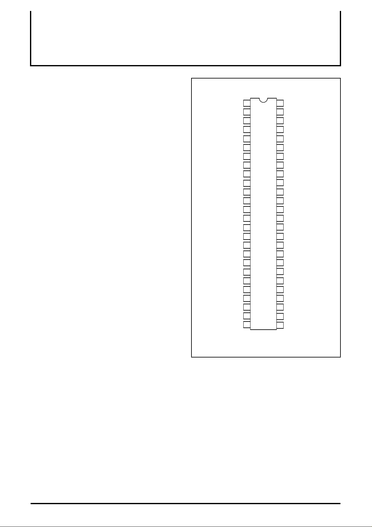
Outline 52P4B
52
49
50
51
1
4
3
2
485
476
449
43
10
42
11
4112
13
14
40
39
7
8
46
45
15
38
16 37
17 36
18 35
19
20
34
33
21 32
22 31
23
24
30
29
25
28
26
27
M52779SP
AFT OUT
LIMITER IN
RF AGC OUT
IF AGC FILTER
VIF GND
VIF IN
VIF IN
VIF VCC
H VCC
RAMP AGC
SCL
SCP OUT
H OUT
SDA
H OSC
AFC 1 FILTER
I REF
+RAMP OUT
-RAMP OUT
Hi VCC
R OUT
G OUT
B OUT
VCD V
CC
B IN
CONTRAST CONT.
VIDEO OUT
VIDEO APC FILTER
VCO
VCO
FM DIRECT OUT
EXT AUDIO IN
AUDIO OUT
- (R-Y) IN
- (B-Y) IN
- (R-Y) OUT
SECAM REF.
- (B-Y) OUT
X-TAL 4.43
SYNC SEP IN
Y SW OUT
VCD GND
TV IN
CHROMA APC FILTER
EXT IN
AUDIO BYPASS
X-TAL 3.58
FAST BLK
KILLER FILTER
R IN
AFC2 FILTER
G IN
MITSUBISHI ICs (TV)
M52779SP
VIF, SIF, VIDEO, CHROMA, DEFLECTION FOR PAL/NTSC
DESCRIPTION
The M52779SP is a single-chip semiconductor integrated circuit to
process signals of a color TV. Circuits to process video IF, sound IF,
video, color, and deflection signals, a I
2
C bus control circuit, and D/
A are build in this device.
This IC can be used not only for popular-type TV sets but also for
middle-class TV sets. Combined with a SECAM chroma decoder,
the M52325AP, this de vice can process signals of every type of TVs
in the world by discriminating them fully automatically.
FEATURES
•
A built-in I
number of peripheral parts and rationalize production lines.
Various filters (TRAP, BPF, Y-DL, RGB clamp) are build in this IC.
•
PLL detection system is introduced to process video IF and voice
•
IF. Furthermore, AFT coil is not necessary.
DL aperture control
•
Color signal frequency and vertical frequency of TVs of every
•
type can be discriminated fully automatically.
•
Horizontal/vertical countdown system
•
V-Ramp output
•
RGB output
•
Built in Y/C SW
2
C bus control circuit makes it possible to reduce the
APPLICATION
PAL/NTSC CTV
PIN CONFIGURATION (TOP VIEW)
RECOMMENDED OPERATING CONDITION
Supply voltage................................................V8, 24=5V, V9, 20=8V
Rated supply voltage........................................V8, 24=4.75 to 5.25V
V9, 20 =7.6 to 8.4V
Maximum output current.............................................5.0mA (pin13)
1
Page 2
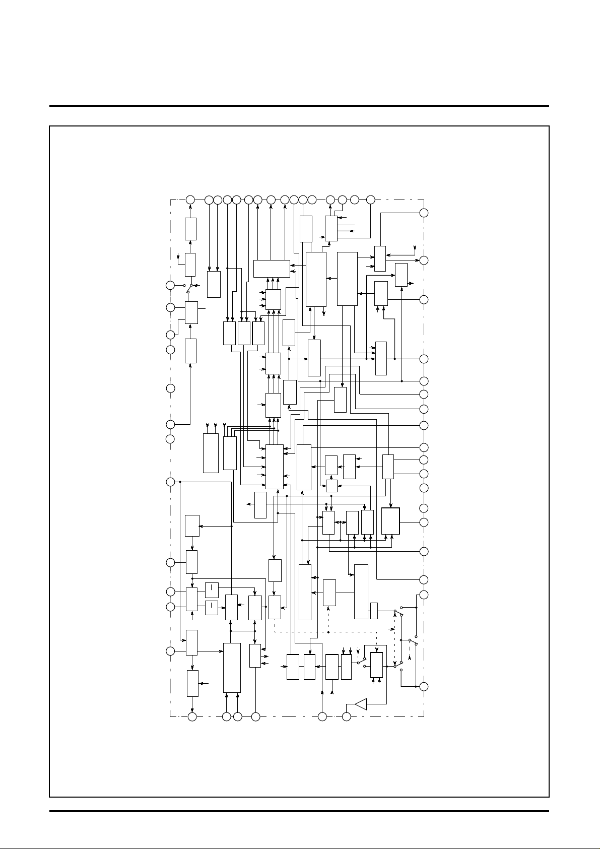
BLOCK DIAGRAM
EXT AUDIO IN
AUDIO BYPASS
FM DIRECT OUT
LIMITER IN
VIDEO OUT
VIF GND
VIF V
CC
Hi VCC
AUDIO ATT
47
3348552
8
2
20
AUDIO OUT
SDA
46
14
AF
AMP
ATT
BUS
AUDIO SW
FM
4.5/6.0
DET
LIMITER
SYSTEM SET
SYSTEM
DET
LOCK
FAST BLK
SCL
B IN
25
31
11
I / F
B EXT
INPUT
SYSTEM auto
peak ACL
ACL
DECODE
MITSUBISHI ICs (TV)
M52779SP
VIF, SIF, VIDEO, CHROMA, DEFLECTION FOR PAL/NTSC
CC
G OUT
22
BLK
CLAMP
V SYNC
AMP
SYNC
BRIGHT
MATRIX
CONTRAST
SECAM REF.
G IN
42
27
REF
SECAM
TRIG
EQ
SEP
CHROMA
CONTRAST
DEMODULATOR
H V
-RAMP OUT
9
19
RAMP
SERVICE SW
VERTICAL
COUNT DOWN
50/60 OUT
ELIMINATE
PAL
F/F
DET
KILLER
I REF
+RAMP OUT
17
18
V-SIZE
HORIZONTAL
COUNT DOWN
BGP
GENE
SW
CONT
PHASE
Acc
DET
RAMP AGC
10
V-POSITION
AFC-2
H STOP
32FH
AFC GAIN
(H.FREEADJ)
TINT
ID
DET
VCO
AFC-1
VCXO
APC
CHROMA
MUTE
DET
AFC2 FILTER
28131516
H-PHASE
H OUT
DET
MUTE
OUT
H OSC
AFC 1 FILTER
SCP OUT
12
- (B-Y) IN
44
- (R-Y) IN
45
- (B-Y) OUT
- (R-Y) OUT
43
X-TAL 3.58
32
X-TAL 4.43
40
VCD GND
37
VCD V
24
CHROMA APC FILTER
35
CC
INPUT
R EXT
ID OUT
R IN
R OUT
21
29
RGB
CUT OFF
INPUT
G EXT
RB
DRIVE
BRIGHT
SERVICE
COLOR
SYSTEM
B OUT
23
HV
DRIVE
RGB
ID
VIDEO APC FILTER
VCO
VCO
IF AGC FILTER
KILLER FILTER
30
51
SW
44
ππ
VCO
ADJ
VCO
IF AGC
RF AGC
3
+–
DELAY ADJ
6
VIF IN
DET
VIDEO
VIF
AMP
7
VIF IN
50
49
4
APC
DET
POS/NEG
AFT
1
AFT OUT
REF
FILTER
ADJ
DET
AFT OUT
DEFEAT
MUTE
VIDEO
VIDEOMUTE
2ND AMP
CLAMP
CONTRAST
BPF
CHROMA
DL
TONE
VIDEO
SHARPNESS
26
(ACC)
1ST AMP
SW
DL
FINE
TIME
TRAP
DELAY
X2
38
Y SW OUT
HPF
IN
Y/C
TRAP
CHROMA
F.TRAP
D.TRAP
SW4
SW2
39
34
SW1
TV/EXT
36 41
SYNC SEP IN
EXT IN
TV IN
RF AGC OUT
CONTRAST CONT.
2
Page 3
∗
°
°
VIF, SIF, VIDEO, CHROMA, DEFLECTION FOR PAL/NTSC
ABSOLUTE MAXIMUM RATINGS
Symbol Parameter Ratings Unit
V
CC
P
d
T
opr
T
stg
S
urge
2
I
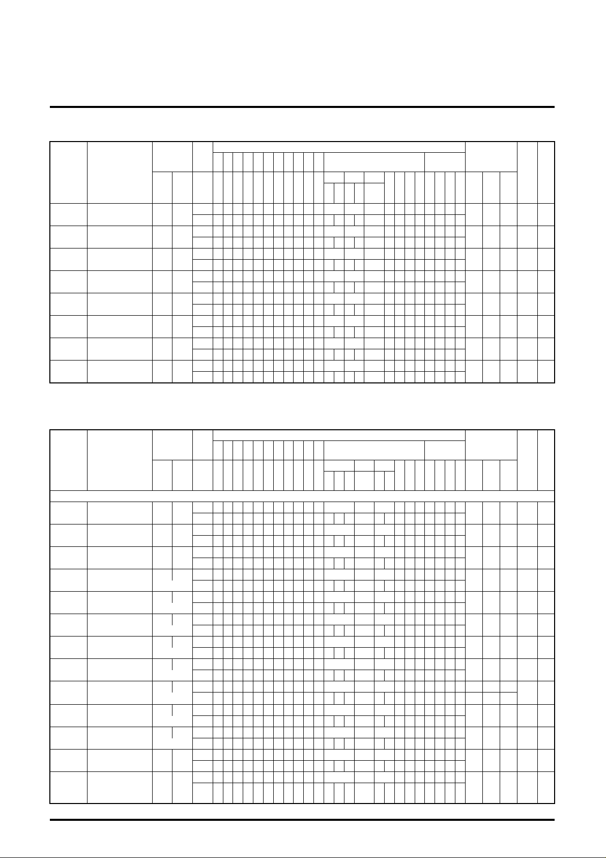
C BUS DEFAULT CONDITION OF ALL BLOCKS IN M52779SP
All
Blocks
Supply voltage 6.0, 9.0 V
Power dissipation 1.69 W
Operating temperature -20 to +65
Storage temperature -40 to +150
Electrostatic discharge -200 to +200 V
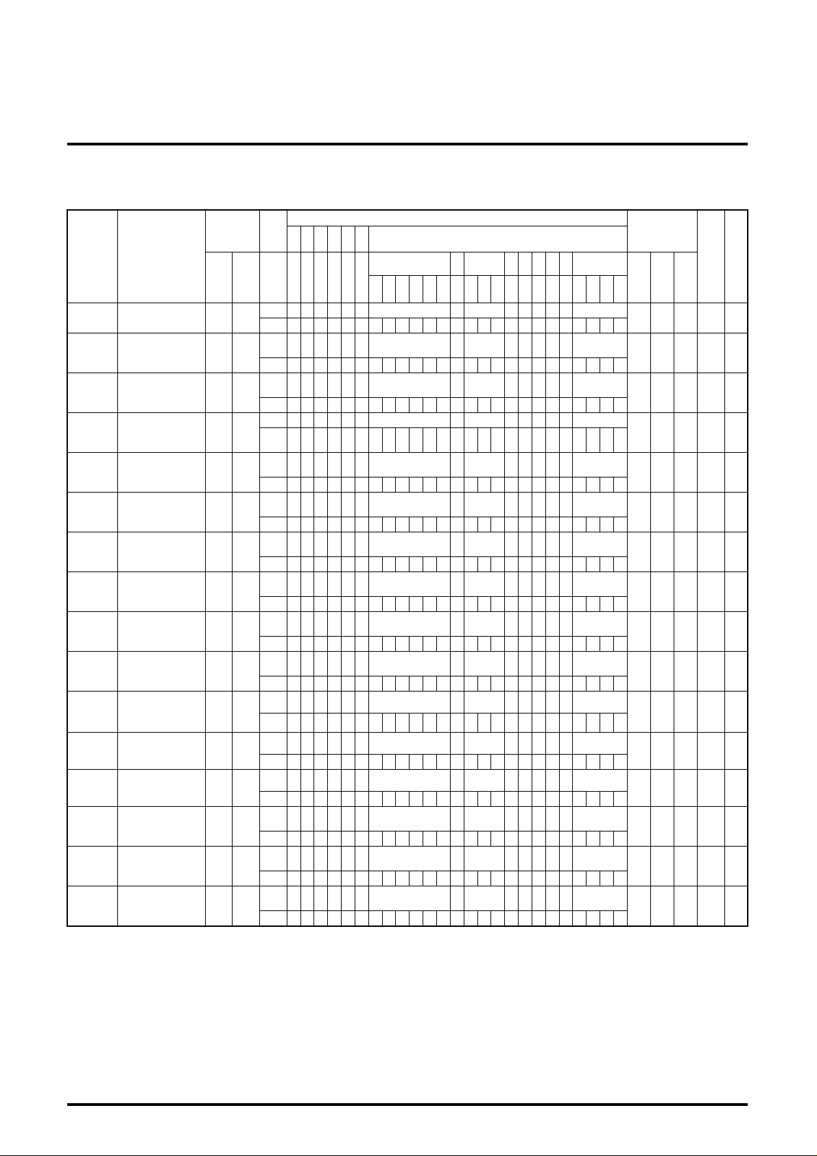
sub address 00H 01H 02H 03H 04H 05H 06H 07H
function DLA P/N
VCOA AVSW
Y/C
4.5/6.0
DFA
TRF2
DBF
TRAP
DATA 20H 20H 00H 40H 00H 20H 02H 40H
function 32 0 32 0000000064003220064
C
C
VidG ATT
−
−
MITSUBISHI ICs (TV)
M52779SP
SHARP
DEFE
CONT
DLTA
TV/EXT
AUTO
TINT
sub address 08H 09H 0AH 0BH 0CH 0DH 0EH 0FH 10H 12H 13H
All
Blocks
function
COLOR
SET HP BRI DR
DATA 20H 40H 20H 20H 20H 10H 10H 10H 60H 00H 40H
function 32 0 8 32 32 0 32 16 16 16 011010000
MUTE
DB CR CG CB V-PO TRF HA
Please refer to the following sub-address data for each parameter you measure.
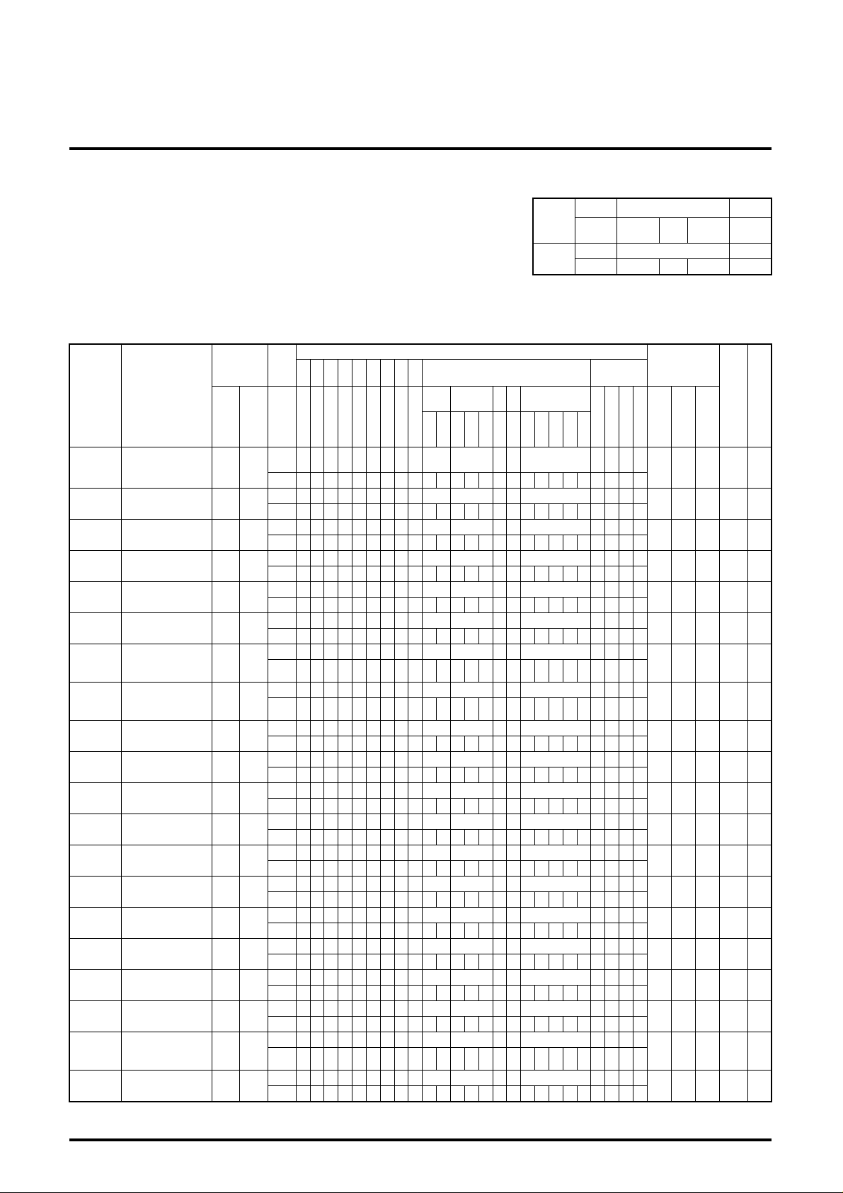
ELECTRICAL CHARACTERISTICS
Input signal SW
Symbol Parameter
Input SG PIN
Supply current
−
I
CC8
I
CC24
CC9
I
I
CC20
VIF block
−
Vdc
NEG
Vdc
POS
Vo
NEG
Vo
POS
P/N Video S/N V SG3
f
V
Default conditions of
supply current
Pin8, 24
supply current
Pin9
supply current
Pin20
supply current
Default conditions
of VIF
Video detector output
DC voltage (NEG)
Video detector output
DC voltage (POS)
Video detector output
AC voltage (NEG)
Video detector output
AC voltage (POS)
Video frequency
characteristics
−−
−−
−−
−−
−−
−−
−−
V SG1
V SG2
V SG4
(Ta=25 ° C, pin8 and pin24:5V supply/pin9 and pin20:8V supply unless otherwise noted.)
Test conditions
S4S
16
P1P3P4P12P13P16P18P19P46P48P
SW 1 1 0 0 20H 20H 40H
PIN 32 0 32 0 64
SW
PIN
SW
PIN
SW
PIN
SW 1 1 0 0 20H 20H 00H
PIN 320320 0
SW
PIN
GND
SW 60H
PIN
GND
SW 0
PIN M
SW 0 60H
PIN M 1
SW 0
PIN M
SW 0
PIN M
S44S
45
DLAP/NVC
52
M
M1
Sub address function
00H 01H 03H
AV
ATT
S
OA
W
SUBPO
ACL SER HST
V
CC
P8P9P20P
5V 8V 8V 5V
MM
M
5V 8V 8V 5V
Min. Typ. Max.
24
−
70 110 150 mA
50 60 70 mA
5.5
M
−
4.3
1.6
1.9
1.9
50 55
4.5 5.5
AFCG
Limits
−
−
10.0
15.0
−
−
4.7 5.1 V
2.0 2.4 V
2.2 2.5 V
2.2 2.5 V
ACL
Unit Note
−
PIN8+
PIN24
mA
−
dB
MHz
3
Page 4
−
µ
SW −
SW −
SW −
−
MITSUBISHI ICs (TV)
M52779SP
VIF, SIF, VIDEO, CHROMA, DEFLECTION FOR PAL/NTSC
−
ELECTRICAL CHARACTERISTICS
Input signal SW
Symbol Parameter
Input SG PIN
Vin
min
Vin
max
GR
V4H
V4T
V4L
V1
Input sensitivity V SG5
Maximum
permissible input
AGC control
range
Maximum IF
AGC voltage
IF AGC voltage
(80dBu)
Minimum IF
AGC voltage
AFT defeat
voltage
AFTNAFT detector
sensitivity (NEG)
V1H
N
V1L
N
V3H
V3L
CRU
CRL
CRT
Maximum AFT
voltage (NEG)
Minimum AFT
voltage (NEG)
Maximum RF
AGC voltage
Minimum RF
AGC voltage
Capture range
(upper)
Capture range
(lower)
Capture range
(total)
IM Intermodulation V
DG
DP
DG
DP
SPN Sync ratio (NEG) V
DLPH
DLPL
Maximum delay
point (NEG/POS)
Minimum delay
point (NEG/POS)
SIF block
−
Default conditions
of SIF
VAF AF output (DC) S
VoAF
N
VoAF
P
VoAF
S
AF direct output
(4.5M)
AF direct output
(5.5M)
AF direct output
(6.0M)
V SG6
−−
−−
V SG7
V SG8
−−
V
V
V
V SG3
V SG8
V SG9
V SG9
−−
V
V
V
V
−−
S
S
S
SW 0
PIN M
SW 0
PIN M
SW
PIN
SW 0
PIN M
SW 0
PIN M
SW 0
PIN M
SW
PIN M
SW 0
SG9
PIN M
SW
SG10
PIN M
SG11
PIN M
SW
PIN M
SW
PIN M
SW
PIN M
SW
PIN M
SW
PIN
SW
SG12
PIN M
SG13
PIN M
SG13
PIN M
SW
SG13
PIN M
SW
SG14
PIN M 0
SW
SG15
PIN M 63
SW 1 1 0 0 20H 20H 40H
PIN 32 0 32 0 64
SW
SG21
PIN M
SW
SG16
PIN M
SW
SG17
PIN M
SW
SG18
PIN M
(cont.)
S4S
16
P1P3P4P12P13P16P18P19P46P48P
S44S
45
Test conditions
Sub address function
00H 01H 03H
DLAP/NVC
52
OA
00/40H
0/1
3F/7FH
0/1
V
CC
Limits
Unit Note
AV
ATT
S
W
P8P9P20P
Min. Typ. Max.
24
47 52 dB µ
102 107 − dB µ
50 60 − dB µ
calcu-
late
4.0 4.4 4.8 V
2.2 2.6 3.0 V
1.5 1.9 2.3 V
3.7 4.0 4.3 V
43 61 79
mV/
kHz
7.2 7.7 − V
0.3 0.8 V
7.2 7.7 − V
0.3 0.8 V
0.8 1.2 − MHz
2.2 2.6 − MHz
3.0 3.8 − MHz
calcu-
late
31 36 − dB
3 7 %
3 7 deg
25.0 28.5 32.0 %
90 96 − dB µ
70 76 dB µ
5V 8V 8V 5V
−−−−
2.0 2.4 2.8 V
400 570 740
430 570 710
440 590 740
mVrms
mVrms
mVrms
4
Page 5
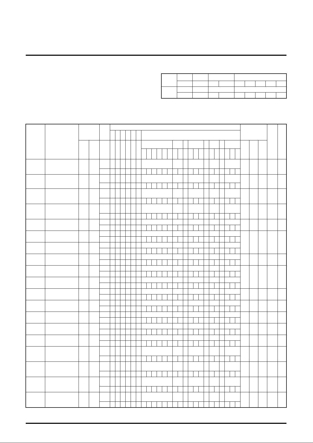
ELECTRICAL CHARACTERISTICS (cont.)
Input signal SW
Symbol Parameter
Input SG PIN
VoAF
M
VoAF
max
ATT
THD
AF
LIM
AF direct output
(6.5M)
Maximum AF
output (6.0M)
Maximum
attenuation (6.0M)
AF output
distortion (6.0M)
Input limiting
sensitivity
S
S
S
S
S
AMR AMR S
AFSN AF S/N S
GEAu EXT audio GAIN EXT
SG19
SG18
SG18
SG18
SG18
SG20
SG21
SG22
S4S
P1P3P4P12P13P16P18P19P46P48P
SW
PIN M
SW 7FH
PIN M 127
SW 00H
PIN M 0
SW
PIN M
SW
PIN M
SW
PIN M
SW
PIN M
SW 60H 48H
PIN M 32 1 72
MITSUBISHI ICs (TV)
M52779SP
VIF, SIF, VIDEO, CHROMA, DEFLECTION FOR PAL/NTSC
Test conditions
16
45
S44S
Sub address function
00H 01H 03H
DLAP/NVC
52
OA
VCC
AV
ATT
S
W
P8P9P20P
Limits
Min. Typ. Max.
24
460 615 770
1140
860
59 68 − dB
− 1 3 %
− 40 46 dB
49 50 − dB
53 63 − dB
-2.0 0.0 2.0 dB
1420
Unit Note
mVrms
mVrms
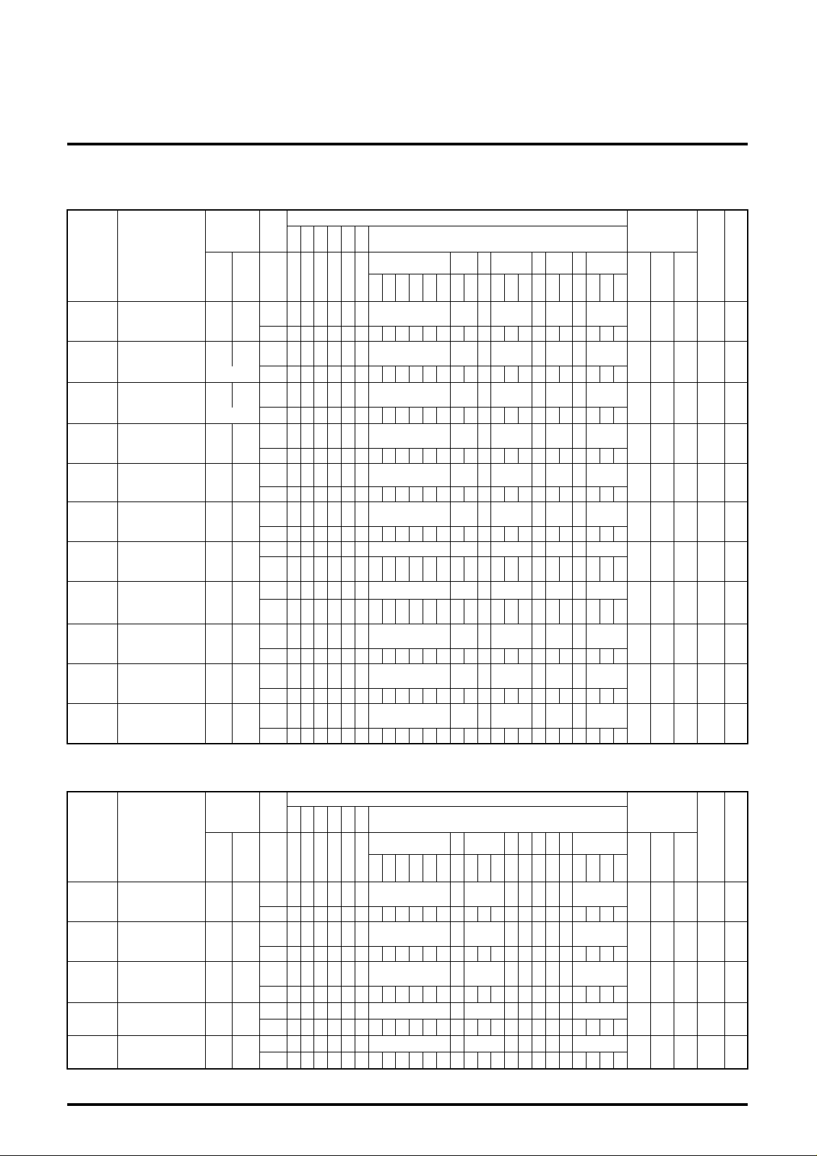
ELECTRICAL CHARACTERISTICS (C0 to C12:input SG50 at SY IN C13 to C21:input SG60 at SY IN)
M
Test conditions
Sub address function
06H 07H 09H
TV/
DL
43
AU
EX
TA
TO
T
TINT
VCC
SE
H
T
P
P8P9P20P
5V 8V 8V 5V
Symbol Parameter
chroma block (PAL)
−
Cn1
Cn2
A
CC1 ACC 1
CC2 ACC 2
A
Default conditions
of chroma
Output signal
amplitude 1:- (B-Y)
Output signal
amplitude 2:- (R-Y)
OV Chroma overload
VikP
killP
APC1
R/BP
θR-Y
P
CC
Threshold color
killer on
Residual color
leakage at killer on
APC pull in
range 1
Ratio of
(R-Y/B-Y)
Demoduration
phase θR-Y
Residual carrier
leakage
Offset of
DDH
demodulated
output by line
Input signal SW
Input SG PIN
−−
SS4P
VI
SS4P
VI
VS4P
VI
S4S
16
S44S
45
P1P3P4P12P13P16P18P23P41P42P
SW 1 1 0 0 02H 2FH 40H
PIN 2 0 0 47 0 8
SW
PIN M
SW
PIN M
SW
v=+6dB PIN M
VS4P
VI
SW
v=-20dB PIN M
VS4P
VI
SW
eb=800mV PIN M
VS4P
VI
SW
v=variable PIN M
VS4P
VI
SW
v=-40dB PIN M
VS4P
VI
f=variable
VI
eb=monochroma
VI
eb=monochroma
VI
SW
PIN
VS4P
SW
PIN M M
VS4P
SW
PIN M M
SW
SS4P
PIN M
4.2M SW
VI
sin
PIN M
wave
Limits
Min. Typ. Max.
24
−
−
480 680 880
390 530 670
-3 0 3 dB
-3 0 3 dB
1 3 5 dB
− -37 -33 dB
0 30 60
+300 +550
-300 -450
0.45 0.6 0.75 −
80 90 100 deg
0 50 100
− − 100 mV
−
−
−
Unit Note
−
mVP-P
mVP-P
mVP-P
f=eb
Hz
=ec
50kHz
50kHz
mVP-P
eb=
ec+
eb=
ec+
5
Page 6
ELECTRICAL CHARACTERISTICS (cont.)
Symbol Parameter
chroma block (NTSC)
Cn3
Cn4
VikN
killN
APC2
R/BN
θR-Y
N
Output signal
amplitude 3:- (B-Y)
Output signal
amplitude 4:- (R-Y)
Threshold color
killer on
Residual color
leakage at killer on
APC pull in
range 2
Ratio of
(R-Y/B-Y)
Demoduration
phase θR-Y
TC1 Tint control 1
TC2 Tint control 2
chroma block (others)
SRA
SRD
SECAM ref
output amplitude
SECAM ref output
DC voltage
System
AUTO 1
identification 1
4.43 PAL
System
AUTO 2
identification 2
4.43 NTSC
System
AUTO 3
identification 3
3.58 PAL
System
AUTO 4
identification 4
3.58 NTSC
System
AUTO 5
identification 5
SECAM
System
AUTO 6
identification 6
black & white
Input signal SW
Input SG PIN
SS3N
VI
SS3N
VI
VS3N
VI
v=variable PIN M 6
VS3N
VI
eb=0mV PIN M 6
VS3N
VI
f=variable PIN M
VS3N
VI
eb=monochroma
VS3N
VI
eb=monochroma
VS3N
VI
eb=monochroma
VS3N
VI
eb=monochroma
−−
−−
SS4P
VI
SS4N
VI
SS3P
VI
SS3N
VI
−−
−−
S4S
P1P3P4P12P13P16P18P23P41P42P
SW 46H
PIN M 6
SW 46H
PIN M 6
SW 46H
SW 46H
SW
SW 46H
PIN M 6
SW 46H
PIN M 6
SW 7FH 46H
PIN M 127 6
SW 00H 46H
PIN M 0 6
SW 41H
PIN M 1
SW 41H
PIN M 1
SW 25H
PIN M 1 1 1
SW 25H
PIN M 1 1 1
SW 25H
PIN M 1 1 1
SW 25H
PIN M 1 1 1
SW 25H
PIN M
SW 25H
PIN M 1 1 1
MITSUBISHI ICs (TV)
M52779SP
VIF, SIF, VIDEO, CHROMA, DEFLECTION FOR PAL/NTSC
Test conditions
16
45
S44S
Sub address function
06H 07H 09H
TV/
DL
43
AU
EX
TA
TO
T
TINT
VCC
SE
H
T
P
P8P9P20P
5V 8V 8V 5V
46H
5V 8V 8V 5V
150
111
µA
Limits
Min. Typ. Max.
24
470 670 870
320 480 620
− -46 -38 dB
0 30 60
+350 +870
-1000
-350
0.4 0.6 0.8 −
80 95 110 deg
25 45 60 deg
25
45
200 400 570
3.8 4.3 4.8 V
0001
−
0101
−
1001
−
1101
−
0011
−
− --00 −
Unit Note
mVP-P
mVP-P
mVP-P
−
Hz
−
60 deg
mVP-P
−
−
−
−
−
eb=
ec+
50kHz
bus
data
read
mode
bus
data
read
mode
bus
data
read
mode
bus
data
read
mode
bus
data
read
mode
bus
data
read
mode
6
Page 7
MITSUBISHI ICs (TV)
M52779SP
VIF, SIF, VIDEO, CHROMA, DEFLECTION FOR PAL/NTSC
Sub
address
No.
function COLOR DR MUTE ACL
DATA 00H 20H 47H
Y
0
function 0 32 0 15 0 0 0
ELECTRICAL CHARACTERISTICS
Video & RGB I/F block (∗ input SG50 at SY IN. (Y5 to Y7, Y36 to Y46:input SG60.)/VCC:P8, P24=5V.P9, P20=8V)
Input signal SW
Symbol Parameter
Input SG PIN
−
Ymax
GY
FBY
2AGY
CTR1
TRF1
DTR1
CTR2
TRF2
DTR2
Default conditions of
video & RGB I/F
Maximum video
amplitude
Video gain
Video frequency
characteristics
Pin 38 output
amplitude
Chroma trap
attenuation 1
Chroma trap fine
adj. attenuation 1
Chroma double trap
attenuation 1
Chroma trap
attenuation 2
Chroma trap fine
adj. attenuation 2
Chroma double trap
attenuation 2
−−
VI SGA
VI SGA
VI SGB
VI SGA
VI SGF
VI SGF
VI SGF
VI SGB
VI SGB
VI SGB
YDL1 Y delay time 1 VI SGA
YDL2 Y delay time 2 VI SGA
YDL3 Y delay time 3 VI SGA
YDL4 Y delay time 4 VI SGA
GTnor Video tone 1 VI SGB
GTmax Video tone 2 VI SGB
GTmin Video tone 3 VI SGB
GT2M Video tone 4 VI SGB
S4S16S44S
45
P21P22P23P26P38P
4.5
40
DF
/
6.0
SW1100 00H 00H
PIN 00000000322006408
SW
PIN M M M
SW
PIN M M M 64
SW 33H
PIN M 51 64
SW 46H
PIN M 6 8
SW 00/20H 33H 46H
PIN M M M
SW 20/28H 33H 46H 00/60H
PIN M M M
SW 30H 33H
PIN M M M 1 1 51
SW 00/20H 33H
PIN M M M
SW 20/28H 33H 00/60H
PIN M M M
SW 30H 33H
PIN M M M 1 1 51
SW 00H
PIN M M M 0
SW 01H
PIN M M M 1
SW 02H
PIN M M M 2
SW 03H
PIN M M M 3
SW 20H
PIN M M M 32 50
SW 3FH
PIN M M M 63 50
SW 00H
PIN M M M H 50
SW 20H
PIN M M M 32 50
Test conditions
Sub address function
02H 04H
TR
DB
A
F2
0/1 151 68
0/1 151
SH
TRAPVid
DEFPCO
AR
F
G
P
0/1
51 6 8
0/1 51
08H 0BH 13H
05
06H
H
TV/
DL
AU
EX
NT
TA
TO
T
20
02H
H
7F
H
127
40
H
40
H
32
H
32
H
32
H
32
H
0A
H
BRYSE
40
H
09H
T
40H
HP DB
0C
10H
H
V-POTR
F
20
60H
H
32011
0/1
0/1
Min. Typ. Max.
HA
3.2 4.1 4.9 VP-P
8 11 14 dB
-4 0 − dB
1.5 2.1 2.7 VP-P
−
−
−
−
155 240 325 nsec
135 220 265 nsec
250 380 450 nsec
345 500 605 nsec
1.1 1.6 2.1 V
0 3.6 6.7 dB
-10 -4 -1 dB
-2.0 1.0 4.0 dB
SER HST AFCG
Limits
Unit Note
-18 dB
−
-20 dB
−
-18 dB
−
-20 dB
−
P-P
7
Page 8
ELECTRICAL CHARACTERISTICS
Video & RGB I/F block (cont.)
Input signal SW
Symbol Parameter
Input SG PIN
GT5M Video tone 5 VI SGB
GYnor Contrast 1
VI SGB SW
f=100kHz
GYmin Contrast 2
VI SGB SW
f=100kHz
Lumnor Bright 1
Lummax Bright 2
Lummin Bright 3
−−
−−
−−
D (R) Drive R VI SGA
D (B) Drive B VI SGA
EX (R) EXT (R) I/O
EX (G) EXT (G) I/O
EX (B) EXT (B) I/O
FB
ER
FB
EG
FB
EB
SW 20H
PIN M M M 32 50
PIN
PIN
SW
PIN M M M 64
SW
PIN M M M
SW
PIN M M M 0
SW
PIN
SW
PIN
SW 0
SGD
PIN M
SW 0
SGD
PIN M
SW 0
SGD
PIN M M
MITSUBISHI ICs (TV)
M52779SP
VIF, SIF, VIDEO, CHROMA, DEFLECTION FOR PAL/NTSC
Test conditions
S4S16S44S
45
P21P22P23P26P38P
02H 04H
4.5
40
TR
DF
DB
/
A
F2
6.0
Sub address function
SH
TRAPVid
AR
F
G
P
DEFPCO
05
06H
H
TV/
DL
AU
EX
NT
TA
TO
T
32
H
40
H
0A
H
BRYSE
09H
T
HP DB
0C
10H
H
V-POTR
F
MMM 64
00
H
MMM 0
40
H
7F
H
127
00
H
00/3FH
M0/
M0/
7F
H
127
7F
H
127
7F
H
127
63
00/
3FH
63
00
H
0
00
H
0
00
H
0
Limits
Min. Typ. Max.
HA
-4 -1.4 -1.2 dB
2.1 2.5 2.9 V
−
−
1.1 1.4 1.8 V
0.6 1.0 1.4 V
-1.4 -1.0 -0.6 V
2.9 5.5 7.1 dB
2.9 5.5 7.1 dB
4.8 6.0 7.2 V
4.8 6.0 7.2 V
4.8 6.0 7.2 V
Unit Note
P-P
50 mV
P-P
P-P
P-P
Video & RGB I/F block (cont.)
Input signal SW
Symbol Parameter
Input SG PIN
OFRG
OFBG
C (R) Cut off R
C (G) Cut off G
C (B) Cut off B
Offset voltage
R-G
Offset voltage
B-G
−−
−−
−−
−−
−−
Test conditions
S4S16S44S
45
P21P22P23P26P38P
02H
4.5
40
TR
DF
DB
/
A
F2
6.0
Sub address function
05
H
TRAPVid
CONTDL
F
G
06H
TV/
TA
08H0AH0DH0EH0F
CO
AU
EX
LO
TO
T
R
SW
PIN M 64
SW
PIN M M 64
SW
PIN M 64
SW
PIN M
SW
PIN M
BR
I
40
H
40
H
40
H
CR CG CB
00/
FFH
0/
255
00/
FFH
0/
255
H
ACLSERHSTAF
00/
FFH
0/
255
13H
CG
-160 0 160 mV
-160 0 160 mV
Limits
Unit Note
Min. Typ. Max.
1.0 1.4 1.8 V
1.0 1.4 1.8 V
1.0 1.4 1.8 V
8
Page 9
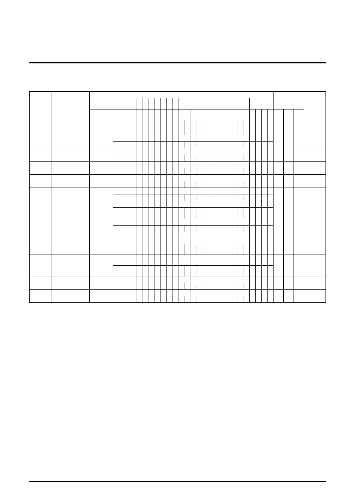
ELECTRICAL CHARACTERISTICS
Video & RGB I/F block (cont.)
Input signal SW
Symbol Parameter
Input SG PIN
DLF
Y delay time
〈fine〉
VI SGA
Ccon1 Color control 1 -R SGE
Ccon2 Color control 2 -R SGE
VMF Video mute VI
MTXB Matrix 1 -B SGE
MTXG Matrix 2 -B SGE
MTXR Matrix 3 -R SGE
MTXG1 Matrix 4 -R SGE
OSD1 OSD speed 1
OSD2 OSD speed 2
ER,EG
EB,FB
ER,EG
EB,FB
GYmax1 Contrast 3 VI SGA
GYmin1 Contrast 4 VI SGA
ABR
Bright control
〈VCC=8.5V at pin20〉
−−
PACL1 Peak ACL 1 VI SGB
PACL2 Peak ACL 2 VI SGB
PACL3 Peak ACL 3 VI SGB
SW 02H 03H
PIN M M M 1 3
SW 1 1
PIN M
SW 1 1
PIN M 0 72
SW
SGB
f=4.43M
PIN M M M
SW 1 1 20H
PIN M 1 50 64
SW 1 1 20H
PIN M 1 50 64
SW 1 1 20H
PIN M 1 50 64
SW 1 1 20H
PIN M 1 50 64
SW
SGD
PIN M M M 0
SW
SGD
PIN M M M 0
SW
PIN M M M
SW
PIN M M M
SW
PIN M
SW
PIN M
SW
PIN M
SW
PIN M
S4S16S44S
45
P21P22P23P26P38P
2.9
V
0V
MITSUBISHI ICs (TV)
M52779SP
VIF, SIF, VIDEO, CHROMA, DEFLECTION FOR PAL/NTSC
Test conditions
Sub address function
08H0A
AU
TO
CO
LO
R
7F
H
127
00H48
40
H
40
H
40
H
40
H
00
H
00
H
H
BR
I
48
H
72
H
7F
H
127
7F
H
127
7F
H
127
7F
H
127
0DH0EH0F
CR CG CB
7F
H
127
20H20H20
13H
H
ACLSERHSTAF
00H
H
06H
TV/
EX
TA
T
00H
0 3232320000
00H
20H20H20
40H
H
0 3232328000
00H
20H20H20
47H
H
0 32323215 0 0 0
F
TRAPVid
G
05
H
CONTDL
32
H
32
H
32
H
32
H
7F
H
127
7F
H
127
7F
H
127
7F
H
127
7F
H
127
02H
4.5
40
TR
DF
DB
/
A
F2
6.0
Limits
Min. Typ. Max.
CG
9 45 65 nsec
150 310 500
− 10 150
− -50 -40 dB
0.5 0.8 1.2 VP-P
80 190 300 mVP-P
0.5 0.8 1.2 VP-P
200 400 600 mVP-P
− 20 90 nsec
− 50 160 nsec
3.7 4.6 6.3 VP-P
− 0 50 mVP-P
2.0 −−V
1.0 2.0 3.0 V
3.2 4.2 5.2 V
3.4 4.4 5.4 V
Unit Note
mVP-P
mVP-P
0BH
A0/A7
MUTE
:0/1
P20=
8.5V
9
Page 10
MITSUBISHI ICs (TV)
M52779SP
VIF, SIF, VIDEO, CHROMA, DEFLECTION FOR PAL/NTSC
ELECTRICAL CHARACTERISTICS
Deflection block
Input signal SW
Symbol Parameter
Input SG PIN
−
ISS
BGP1
BGP2
BGPW
fH
FPH1
FPH2
HPT1
HPT2
HPT3
TH
VH
HSTO
Default conditions
of deflection
Sync. sep. input
sensitivity; current
Burst gate pulse
timing 1 (PAL)
Burst gate pulse
timing 2 (NTSC)
Burst gate
pulse width
Horizontal free-running
frequency
Horizontal pull-in
range 1
Horizontal pull-in
range 2
Horizontal pulse
timing 1
Horizontal pulse
timing 2
Horizontal pulse
timing 3
Horizontal pulse
width
Horizontal pulse
amplitude
Horizontal pulse
stop function
−−
−−
SY SGa
SY SGb
SY SGa
−−
SY
SY
SY SGa
SY SGa
SY SGa
−−
−−
−−
AFCG AFG gain SY SGa
fV
AVER5
SW Service switch
FPV
VW
Vertical free-running
frequency
50/60
identification 5
Vertical pull-in
range
Vertical pulse
width
−−
SY
−−
SY
−−
SW 1 1 0 0 40H 60H
PIN 0801132015000
SW
PIN M
SW
PIN M M
SW
PIN M M
SW
PIN M
SW
PIN M
SW
SGc
f=vari-
PIN M M
able
SW
SGc
f=vari-
PIN M M
able
SW
PIN M M
SW 00H
PIN M M 0
SW 78H
PIN M M 15
SW
PIN M
SW
PIN M
SW 57H
PIN M 1
SW 0 47/67H
PIN M
SW
PIN M
SW
SGd
f70Hz
PIN
SW
PIN M M
SW 11 00
SGd
f=vari-
PIN M
able
SW
PIN M
S4S
16
S44S
45
P12P13P16P18P19P21P22P23P
09H 10H
39
SE
T
Test conditions
Sub address function
11H12
V
V-POTR
HP
HA
F
SIZ
20H00
H
SU
B
ACLSERHSTAF
VP
O
H
Sub
address
No.
function DLTA
DATA 20H 00H
D
0
function 0 0 1 0
VCC
06H 08H
TV/
EXT
Limits
13H
P8P9P20P
CG
47H
5V 8V 8V 5V
Min. Typ. Max.
24
−−−−
− 0.1 0.2 mA
1.5 2.5 3.5 µsec
1.6 2.6 3.6 µsec
4.8 6.0 7.2 µsec
15.3 15.7 16.1 kHz
+580 +780 − Hz
− -440 -220 Hz
7.0 8.1 9.2 µsec
-2.0 -1.4 -0.8 µsec
0.8 1.4 2.0 µsec
21 25 29 µsec
6.7
3 4 − V
3 4 − V
0/1
2.0 4.0 10 dB
41 44 47 Hz
− 70 − Hz
3.5 4 4.5 V
−
0.35 0.52 0.65 msec
AUTO COLOR
65 Hz
−
Unit Note
w-
D7=0
w-
D7=1
10
Page 11
ELECTRICAL CHARACTERISTICS
Deflection block (cont.)
Input signal SW
Symbol Parameter
Input SG PIN
VBLKW
AVER1
AVER2
AVER3
AVER4
WVSS
Rsi1
R∆s1
Rpo1
Rgc
Rpr
Vertical blanking
width (pin21, 22, 23)
50/60
identification 1
50/60
identification 2
50/60
identification 3
50/60
identification 4
Vertical sync.
detection
minimum width
Vertical ramp
size
Vertical ramp
size control
range
Vertical ramp
position control
range
Vertical position
center adjustment
Vertical ramp out
pulse width (PAL)
−−
SY
SY
SY
SY
SY SGd SW
f60Hz width
variable
SY SGA
SY SGA
SY SGA
SY SGA
SY SGA
SW
PIN M M M
SW
SGd
f63Hz
PIN
SW
SGd
f57Hz
PIN
SW
SGd
f53Hz
PIN
SW
SGd
f47Hz
PIN
PIN M
SW
PIN M
SW
PIN M
SW 7F/60H
PIN M
SW
PIN M M
SW
PIN M
VIF, SIF, VIDEO, CHROMA, DEFLECTION FOR PAL/NTSC
S4S
16
P12P13P16P18P19P21P22P23P
S44S
45
09H 10H
39
SE
T
Test conditions
Sub address function
11H12
V
V-POTR
HP
HA
F
SIZ
00/
40
H
0/
64
20
H
31
32
/0
H
SU
B
ACLSERHSTAF
VP
O
13H
CG
MITSUBISHI ICs (TV)
M52779SP
VCC
P8P9P20P
Limits
Min. Typ. Max.
24
1.35 1.5 1.6 msec
− 63 − Hz
− 57 − Hz
− 53 − Hz
− 47 − Hz
9.5
−
1100 1300 mVP-P
900
83 93 103 %
120 170 220 mV
4
−
27 data
520 545 570 µsec
−µsec
Unit Note
w-
D7=1
w-
D7=1
w-
D7=0
w-
D7=0
11
Page 12
MITSUBISHI ICs (TV)
M52779SP
VIF, SIF, VIDEO, CHROMA, DEFLECTION FOR PAL/NTSC
ELECTRICAL CHARACTERISTICS TEST METHOD
P/N Video S/N
1. Input SG3 and measure the rms value of output signal at pin 52.
2. P/N is defined as follows:
0NEG measured value (VP-P) ×10
P/N=20log
V
Measured value (mVrms)
BW Video frequency characteristics
1. Input SG4 and set the frequency f2 to 37.9MHz so that the beat
element of 1MHz is output to pin 52.
2. Then set the applied voltage at pin 4 so that the beat element of
1MHz at pin 52 may be 100dBµ.
3. Decrease f2 to the level at which the beat element becomes 3dB
smaller than the element of 1MHz, and read the value at that
level.
P52
100dBµ
1MHz BW
3
×0.7
(dB)
3dB
IM Intermodulation
1. Adjust the applied voltage at pin 4 so that the lowest output
signal voltage at pin 52 is 2.2V.
P52
2.2V
2. Measure elements of 1.07MHz and 4.43MHz of output at pin 52.
3. IM is defined as follows:
IM=20log
Element of 1.07MHz
Element of 4.43MHz
(dB)
ATT Maximum attenuation
1. Measure the element of 400Hz of output at pin 46.
ATT=20log
2.
V
Measured value
(dB)
0AFmax
LIM Input limiting sensitivity
Decrease the input level of SG 18. Measure the input level when
the element of 400Hz at pin 46 is 3dB smaller than V
0AFM (S6:
Maximum AF output (6.0M)).
Vin min. Input sensitivity
1. Decrease SG5 level until the video detector output is 3dB
smaller then the measured value of Parameter V3 “Video
detector output”.
Vin max. Maximum permissible input
1. Input 90dBu SG6.
2. VA is the output level at pin 52. Increase SG6 voltage until the
output at pin 52 becomes 3dB smaller than VA. The input levell at
that time is the maximum permissible input.
µAFTN AFT detector sensitivity (NEG)
V1HN Maximum AFT voltage (NEG)
V1LN Minimum AFT voltage (NEG)
See the following figure.
P1
5.0V
3.0V
V1HN
37.9Mz 39.9MHzf0
∆f
V1LN
µAFTN is defined as follows:
µAFTN=
(5.0-3.0)×103mV
∆f kHz
(mV/kHz)
AMR
1. Vam is the element of 400Hz at pin 46.
2. AMR is defined as follows:
0AFS (mVrms)
AMR=20log
V
Vam (mVrms)
(dB)
AF S/N
1. Measure the noise (20Hz to 100kHz) of output at pin 46.
2. AF S/N is defined as follows:
AF S/N=20log
0AFmax
Measured value
(dB)
V
GEAu EXT Audio GAIN
Input SG22 at pin 47, and measure the output V
GAIN=20log
Input signal VP-P
Output signal VP-P (pin46)
Cn1 Output signal amplitude 1 (PAL)
Cn2 Output signal amplitude 2 (PAL)
1. Input SS4P to VI IN.
2. Measure output amplitude, Cn1 and Cn2, at pins 41 and 43
f
respectively.
P-P at pin 46.
(dB)
12
Page 13

MITSUBISHI ICs (TV)
M
1H
GND
M
2H
M52779SP
VIF, SIF, VIDEO, CHROMA, DEFLECTION FOR PAL/NTSC
ACC1
1. Input VS4P (eb=570mV:level+6dB) to VI IN.
2. Measure the output amplitude at pin 43.
3. ACC1 is defined as follows:
A
CC1=20log
CC2
A
Measured value (V
Cn1 (VP-P)
P-P)
(dB)
1. Input VS4P (input level:20dB) to VI IN.
2. Measure the output amplitude at pin 41.
CC2 is defined as follows:
3. A
A
CC2=20log
Measured value (V
Cn1 (VP-P)
P-P)
(dB)
OL Chroma overload
1. Input VS4P (ec=800mV
P-P:chroma+3dB) to VI IN.
2. Measure the output amplitude at pin 41.
3. OL is defined as follows:
OL=20log
Measured value (V
Cn1 (VP-P)
P-P)
(dB)
VikP Threshold color killer on (PAL)
1. Input VS4P (level:variable) to VI IN at input level 0dB.
2. Lower the input level whth monitoring the output amplitude at pin
41 and measure the input level when output amplitude isnot
found.
KillP Residual color leakage at killer on (PAL)
1. Input VS4P (level:40dB) to VI IN.
2. Measure the output amplitude at pin 41.
4. R-YP is defined as follows:
V43×3.8
θR-Y P=tan
-1
V41×1.9
+45 (deg)
CC Residual carrier leakage
Measure the element of 4.43MHz of the demodulated output in noinput state.
DDH Offset of demodulated output by line
1. Input 4.2MHz CW (Vi=575mV
P-P) to VI IN.
2. Measure the center DC voltage of output beat amplitude for two
lines at pins 41 and 43. The absolute value of the difference in
DC voltage is the difference of demodulated output on line.
Cn3, Cn4 Output signal amplitude3, 4 (NTSC)
1. Input SS3N to VI IN.
2. Cn3 and Cn4 are output amplitude measured at pins 41 and 43
respectively.
VikN Threshold color killer on (NTSC)
1. Input VS3N (level:variable) to VI IN at input level 0dB.
2. Lower the input level with monitoring the output amplitude at pins
41 and measure the input level when output amplitude is not
found.
APC1 APC pull-in range 1
1. Input VS4P (f=eb=ec=variable) to VI IN.
2. Change the input signal frequency and measure the frequency
range from the point at which signal is output to pin 41 and to the
point that no signal is output to the pin. The reference value is
4.433619MHz.
R/B P Ratio of (R-Y/B-Y)
1. Input VS4P (eb=single chroma=ec+50kHz) to VI IN.
2. V41 is the output amplitude at pin 41.
3. V43 is the output amplitude at pin 43.
4. R /B P is defined as follows:
R/B P=20log
V43 (VP-P)
V41 (VP-P)
(dB)
θR-Y P Demodulation phase
1. Input VS4P (ed=single chroma=ec+50kNz) to VI IN.
2. V41 is the output amplitude at pin 41.
3. V43 is the output amplitude at pin 43.
13
KillN Residual color leakage at killer on (NTSC)
1. Input VS3N (level:-40dB) to VI IN.
2. Measure the output amplitude at pin 41.
APC2 APC Pull-in range 2
1. Input VS3N (f=eb=ec=variable) to VI IN.
2. Change the input signal frequency and measure the frequency
range from the point at which no signal is output to 41 pin and to
the point at which signal is output to the pin. (Pull-in state) The
reference value is 3.579545MHz.
R/B N Ratio of (R-Y/B-Y)
1. Input VS3N (eb=signal chroma=ec+50kHz) to VI IN.
2. V41 is the output amplitude at pin 41.
3. V43 is the output amplitude at pin 43.
4. R/B N is defined as follows:
R/B N=20log
V43 (VP-P)
V41 (VP-P)
(dB)
Page 14

MITSUBISHI ICs (TV)
M52779SP
VIF, SIF, VIDEO, CHROMA, DEFLECTION FOR PAL/NTSC
θR-Y N Demodulation phase
1. Input VS3N (eb=single chroma=ec+50kHz) to VI IN.
2. V41 is the output amplitude at pin 41.
3. V43 is the output amplitude at pin 43.
4. R-YN is defined as follows:
V43×3.8
θR-YN=tan
-1
V41×1.9
+45 (deg)
TC1 Tint control 1, TC2 Tint control 2
1. Input VS3N (see the following figure) to VI IN. Based on the
output voltage at pin 41, find the absolute angle as shown in the
following figure.
-180°
A
0° 90°
B
AUTO1 to 6 System identification1 to 6
Set to AUTO mode and confirm that bus for each output signal is
read correctly.
Ymax Maximum video output
1. Input SGA to VI IN
2. Measure the amplitude (
P-P) except that at blanking part of
output at pins 21, 22 and 23.
M
GY Video gain
1. Input SGA to VI IN
2. Measure the amplitude (
P-P) except that at blanking part of
output at pins 21, 22 and 23. This amplitude is defined as G1.
M =G1
GND
90°
A
B
θ
θ=tan
-1
(B/A)
0°
2. TC is defined as the angle when tint data is center (63).
TCmax is the angle when tint data is max,and TCmin is the
angle when tint data is min.
TC1=TCMAX-TC (deg)
TC2=TC-TCMIN (deg)
SRA SECAM REF output amplitude
SRD SECAM REF output DC voltage
Measure the amplitude (SRA) and DC voltage (SRD) of the element
of 4.43MHz of output at pin 42.
3. GY is defined as follows:
GY=20 log (G1V
P-P/0.714VP-P) (dB)
BW Video frequency characteristics
1. Input SGB (5MHz, 0.4VP-P) to VI IN.
2. Measure the amplitude (P-P) except that at blanking part of the
output at pin 22. The amplitude is defined as YB.
3. BW is defined as follow:
BW=20 log (YB VP-P /GY VP-P) (dB)
2AGY Pin38 output amplitude
1. Input SGA to VI IN.
2. Measure the amplitude (P-P) at pin 38 output.
CTR1 Chroma trap attenuation 1 (common to R/G/B output)
1. Input SS3N to VI IN. Measure the frequency level of 3.58MHz at
trap data 0. The level is defined as N
0.
2. Then, measure the level at trap data 1.
3. CTR1 is defined as follows.
CTR1=20log
Measured value (mVP-P)
N0 (mVP-P)
(dB)
14
Page 15

MITSUBISHI ICs (TV)
M52779SP
VIF, SIF, VIDEO, CHROMA, DEFLECTION FOR PAL/NTSC
TRF1 Chroma trap fine adj. attenuation 1
(common to R/G/B output)
1. Input SS3N to VI IN.
2. Measure the output amplitude of the element of 3.58MHz when
trap fine adj. switch is on. (TRFon)
3. TRF1 is defined as follows.
TRF1=20log
Measure the most attenuation part in three condition of (2), and the
most attenuation part is defined as Y6.
The three condition of (2) is shown below.
condition 1 ON OFF
condition 2 OFF ON
condition 3 ON ON
DTR1 Chroma double trap attenuation 1
(common to R/G/B output)
1. Input SS3N to VI IN.
2. Measure the output amplitude of the element of 3.58MHz when
D.trap swich is on. (DTR on)
3. DTR1 is defined as follows.
DTR1=20log
TRFon (mVP-P)
N0 (mVP-P)
TRAP FINE ADT SW FINE 2
DTRon (mV
N0 (mVP-P)
P-P)
(dB)
(dB)
DTR2 Chroma double trap attenuation 2
1. Input SS4P to VI IN.
2. Measure the output amplitude of the element of 4.43MHz when
D.trap swich is on. (DTR on)
3. DTR2 is defined as follows.
DTR2=20log
Note: In parameters Y5,Y6,Y8 and Y9, limits are defined based on
the maximum attenuation by comparing each one.
YDL1 Y delay time1
1. Input SGA to VI IN.
2. Measure the delay time from signal input to output at pins 21, 22
and 23.
YDL2 to 4 Y delay time2 to 4
1. Input SGA to VI IN.
2. Measure the delay time from signal output at pins 21, 22 and 23
to Y11, YDL1.
DTRon (mV
P0 (mVP-P)
P-P)
(dB)
SGA Output signal
Measure the delay time
at the center point of rise.
M
CTR2 Chroma trap attenuation 2 (common to R/G/B output)
1. Input SS4P to VI IN and measure the frequency level of
4.43MHz at trap data 0. The level is defined as P
2. Then, measure the level at trap data 1.
3. CTR2 is defined as follows.
CTR2=20log
TRF2 Chroma trap fine adj. attenuation 2
1. Input SS4P to VI IN.
2. Measure the output amplitude of the element of 4.43MHz when
trap fine adj. swich is on. (TRFon)
3. TRF2 is defined as follows.
TRF2=20log
Measure the most attenuation part in three condition of (2) , and the
most attenuation part is defined as Y9.
The three condition of (2) is shown below.
condition 1 ON OFF
condition 2 OFF ON
condition 3 ON ON
Measured value (mVP-P)
P0 (mVP-P)
TRFon (mVP-P)
P0 (mVP-P)
TRAP FINE ADT SW FINE 2
(dB)
0.
(dB)
GTnor Video tone 1
1. Input SGB (f=3MHz) to VI IN.
2. Measure output amplitude at pins 21, 22 and 23.
GTmax Video tone 2
1. Input SGB (f=3MHz) to VI IN.
2. Measure output amplitude at pins 21, 22 and 23.
3. GTmax is defined as follows:
GTmax=20log
GTmin Video tone 3
1. Input SGB (f=3MHz) to VI IN.
2. Measure output amplitude at pins 21, 22 and 23.
3. GTmin is defined as follows:
GTmin=20log
GT2M Video tone 4
1. Input SGB (f=2MHz) to VI IN.
2. Measure output amplitude at pins 21, 22 and 23.
3. GT2M is defined as follows:
GT2M=20log
Measured value (VP-P)
GTnor (VP-P)
Measured value (V
GTnor (VP-P)
Measured value (VP-P)
GTnor (VP-P)
P-P)
(dB)
(dB)
(dB)
15
Page 16

MITSUBISHI ICs (TV)
Measure the time lag
Y14
YDL4 signal
Output signal
M
at the center point of rise.
M52779SP
VIF, SIF, VIDEO, CHROMA, DEFLECTION FOR PAL/NTSC
GT5M Video tone 5
1. Input SGB (f=5MHz) to VI IN.
2. Measure output amplitude at pins 21, 22 and 23.
3. GT5M is defined as follows:
GT5M=20log
Measured value (V
GYnor (VP-P)
P-P)
(dB)
GYnor Contrast 1
1. Input SGB (f=100kHz) to VI IN.
2. Measure output amplitude at pins 21, 22 and 23.
GYmin Contrast 2
1. Input SGB (f=100kHz) to VI IN.
2. Measure output amplitude at pins 21, 22 and 23.
Lum nor Brightness control 1, Lum max Brightness control 2,
Lum min Brightness control 3
1. No signal is input. (Only SG50 is input to SY IN.)
2. Measure DC voltage of output at pins 21, 22 and 23 except that
at blanking part.
Output
waveform
M
GND
3. Y23=(Lum max)-(Lum nor), Y24=(Lum min)-(Lum nor)
EXR EXT (R) I/O, EXG EXT (G) I/O, EXB EXT (B) I/O
1. Input SGD to FB, ER, EG and EB.
2. Measure output amplitude which is higher than the pedestal level
at pins21, 22 and 23. The amplitude at blanking part should not
be measured.
M
OFRG Offset voltage R-G, OFBG Offset voltage B-G
1. Measure DC voltage of output at pin 21, 22 and 23 except that at
blanking part .
2. OFRG and OFRB are defines as follows:
OFRG=
(pin 21 Measured voltage)-(pin 22 Measured voltage) (mV)
OFBB=
(pin 23 Measured voltage)-(pin 22 Measured voltage) (mV)
R (C) Cutoff R, G (C) Cutoff G, B (C) Cutoff B
1. Measure DC voltage of output at pin 21, 22 and 23 when R (C),
G (C) and B (C) data are maximum and minimum respectively.
The DC voltage at blanking part should not be measured.
2. R (C), G (C) and B (C) are defined as follows:
R (C), G (C) and B (C)=
(Voltage at data max.)-(Voltage at data min.) (V)
D (R) Drive R
1. Input SGA to VI IN.
2. Measure DRmin and DRmax which are output amplitude at pins
21 at D (R) data min and D (R) data max respectively.
3. G (R) is defined as follows:
G (R)=20log
DRmax (VP-P)
DRmin (VP-P)
(dB)
D (B) Drive B
1. Input SGA to VI IN.
2. Measure DBmin and DBmax which are output amplitude at pin
23 at D (B) data min and D (B) data max respectively.
3. D (B) is defined as follows:
D (B)=20log
DBmax (V
DBmin (VP-P)
P-P)
(dB)
DLF Y delay time 〈fine〉
1. Input SGA to VI IN.
2. Measure the time lag (absolute value) between signal YDL4 and
output signal at pins 21, 22 and 23.
Ccon1 Color control 1, Ccon2 Color control 2
1. Input SGE to -RIN (pin 45).
2. Measure output amplitude at pins 21 under each condition.
VMF Video mute
1. Input SGB to VI IN.
2. Measure output amplitude of the element of 4.43MHz when the
mute switch is on and off. (VMFon, VMFoff)
3. VMF is defined as follows:
VMF=20log
TRFon (VP-P)
TRFoff (VP-P)
(dB)
16
Page 17

MITSUBISHI ICs (TV)
P39 SYNC
HPT1, HPT2, HPT3
P13 H OUT
TH
VH
Measure the output pulse width
at pin 18, when 43kΩ at pin 10
is connected to 8V (VCC).
M52779SP
VIF, SIF, VIDEO, CHROMA, DEFLECTION FOR PAL/NTSC
MTXB Matrix 1, MTXG Matrix 2
1. Input SGE to-B IN (pin 44).
2. Measure output amplitude at pins 22 and 23.
(P23=MTXB, P22=MTXG)
MTXR Matrix 3, MTXG1 Matrix 4
1. Input SGE to-R IN (pin 45 ).
2. Measure output amplitude at pins 21 and 22.
(P21=MTXR, P22=MTXG1)
OSD1 OSD speed 1, OSD2 OSD speed 2
1. Input SGD to FB, ER, EG and EB.
2. Measure rise time and fall time of the signal of output at pins 21,
22 and 23. Measurement points should be higher than the
pedestal level and blanking part should not be measured.
90%
10%
Output waveform at
pins21, 22 and 23.
M
OSD1
M
OSD2
GYmax1 Contrast 3, GYmin1 Contrast 4
1. Input SGA to VI IN.
2. Measure output amplitude at pina 21, 22 and 23 when 2.9V and
0V are extemally applied to pin 26.
ISS Sync separation input sensitivity current
Make current flow out from pin 39 and measure the flow current
when the free running frequency (=45Hz) changed at pin 18 .
BGP1 Burst gate pulse timing 1 (PAL)
BGP2 Burst gate pulse timing 2 (NTSC)
BGPW Burst gate pulse width
FPH1 Horizontal pull-in range 1
FPH2 Horizontal pull-in range 2
Change the frequency of SGc and measure the frequency at the
moment when the output signal at pin 13 and the input signal at pin
39 are pulled in. The horizontal pull-in range is measured by
comparing with 15.625kHz.
HPT1 Horizontal pulse timing 1
HPT2 Horizontal pulse timing 2
HPT3 Horizontal pulse timing 3
HPT2 = Hphase data ( 0 ) - HPT1
HPT3 = Hphase data (15) - HPT1
TH Horizontal pulse width, VH Horizontal pulse amplitude
HSTO Horizontal pulse stop function
Confirm that the horizontal output is high when the horizontal stop
switch is on.
AFCG AFC gain
1. Measure AFC on which is the output amplitude of pin 16 when
AFC switch is on and AFC off which is that when the switch is off .
2. AFCG is defined as follows:
AFCG=20log
AFCon (VP-P)
AFCoff (VP-P)
(dB)
P39 SYNC
BGP1,BGP2
P12 SCP
BGPW
FH Horizontal free running frequency
Measure the output frequency at pin 13 when no signal is input .
17
FV Vertical free running frequency
Measure the output frequency at pin 18 when no signal is input.
SW Service SW operation
Measure the output DC voltage at pin 18 when the service switch
is on.
FPV Vertical pull-in range
Decrease the frequency of SGd and measure the frequency when
output waveform at pin 18 is pulled in.
VW Vertical pulse width (free running)
Page 18

MITSUBISHI ICs (TV)
PIN 13
Horizontal
output
Horizontal
blanking pulse
8
µs
12
µs
4.0V
38.9MHz
Frequency
Voltage
PIN 1 Output waveform
M52779SP
VIF, SIF, VIDEO, CHROMA, DEFLECTION FOR PAL/NTSC
VBLKW Vertical blanking width
Output waveform at
pins 21, 22 and 23
M
GND
AVER5 50/60 identification 5, AVER1 50/60 identification 1
AVER2 50/60 identification 2, AVER3 50/60 identification 3,
AVER4 50/60 identification 4
Confirm that the frequency of output at pin 18 is the same at each
input frequency (pull-in state). Also, confirm the state of the bus
read mode (D7).
WVSS Vertical sync.detection minimum width
Change the input pulse width of SGd and measure the input pulse
width at the moment when the output signal at pin 18 and the input
signal at pin 39 are pulled in.
Rsi1 Vertical ramp size
Measure the pin18 amplitude.
Rs1 Vertical ramp size control range
1. Measure the pin 18 amplitude. (size data : max and min)
2.
Pin18 size max-pin18 size min
Rs1=
Rsi1
×100(%)
Rpo1 Vertical ramp position control range
1. Measure the pin 18 top voltage. ( position data : max and min )
2. Rpo1=pin 18 posi max - pin 18 posi min (mv)
Note: The timing and pulse width of the horizontal blanking pulse
should be as shown in the following figure by adjusting the variable
resistor of the single shot multi vibrator.
The variable resistor at pin 15 of the TTL IC, M74LS221P, is used to
fix the timing at 8µs and that at pin 7 is used to fix the pulse width at
12µs.
∗Coil adjustment
Rgc Vertical position center adjustment
1. Adjust the position bus data so that the output DC bias current at
pin18 and pin 19 should be equal.
2. Specify this position bus data adjusted above.
Rgr Vertical ramp out pulse width (PAL)
Measure the output pulse width
at pin 18, when 43kΩ at pin 10
is connected to 8V (VCC).
VCO COIL
1. Set the test conditions as shown in the parameter V14.
2. Input CW (fo=38.9MHz, Vi=90dBµ) to input pin A.
3. Set the DC voltage at pin 1 (AFT OUT) to 1/2Vcc (4.0V) by
adjusting VCO coil.
Note: VCO coil should always be adjusted as above before using
this IC.
18
Page 19

MITSUBISHI ICs (TV)
M52779SP
VIF, SIF, VIDEO, CHROMA, DEFLECTION FOR PAL/NTSC
(The binary, Decimal and hexadecimal number table)
Hexadecimal
number
Binary number
D3 D2 D1 D0
0 0000 0
1 0001 1
2 0010 2
3 0011 3
4 0100 4
5 0101 5
6 0110 6
7 0111 7
8 1000 8
9 1001 9
A 1010 10
B 1011 11
C 1100 12
D 1101 13
E 1110 14
F 1111 15
(Note)
Hexadecimal Decimal
number
10H = 16
20H = 32
30H = 48
40H = 64
50H = 80
60H = 96
70H = 112
Hexadecimal Decimal
number
90H = 144
A0H = 160
B0H = 176
C0H = 192
D0H = 208
E0H = 224
F0H = 240
80H = 128
Decimal
INITIAL CONDITION
D7 D6 D5 D4 D3 D2 D1 D0 Data
00H
01H
02H
03H
04H
05H
06H
07H
08H
09H
0AH
0BH
0CH
0DH
0EH
0FH
10H
11H
12H
13H
POS/
NEG
00000000
AVSW
00100000
VideoG
TRAP
00000010
00000000
DEFEAT
00100000
00100000
AUTO
00000010
01000000
00100000
HPHASE 3.58
01000000
00100000
MUTE
00100000
00100000
00010000
00010000
00010000
F TRAP
HADJ
00111000
00100000
00000000
AFCG
ACL
01000000
DELAY ADJ
VCO ADJ
FTRAP2
DBF
AUDIO ATT
SHARPNESS
CONTRAST
TINT
COLOR
BRIGHT
DRIVE R
DRIVE B
CUT OFF R
CUT OFF G
CUT OFF B
V-SIZE
SERSW
HST
V-POSI
Y/C DFA
TV/EXT
NTSC
SUB-POSI
ACL
NO
4.5/6.0
DL TIME
SECAM
00H
20H
02H
00H
20H
20H
02H
40H
20H
40H
20H
20H
20H
10H
10H
10H
38H
20H
00H
40H
I2C BUS FORMATS
(1) Slave address: A6 A5 A4 A3 A2 A1 A0 R/W
1 0 1 1 1 0 1 0 (=BAH)
(2) Slave address format:
write
start condition
read
start condition
19
SLAVE ADDRESS SUB ADDRESS DATA BYTE
S
acknowledge bit stop condition
SLAVE ADDRESS DATA BYTE
S
A
acknowledge bit stop condition
AA
A
P
A
P
Page 20

MITSUBISHI ICs (TV)
M52779SP
VIF, SIF, VIDEO, CHROMA, DEFLECTION FOR PAL/NTSC
(3) Sub address byte and data byte format:
write ∗SW
Data byte
0
Service
SW
IF
VIDEO
CHROMA
INTERFACE
DEFLECTION
No. Functions BIT
1 DELAY ADJ 6 00H 0 – A05 A04 A03 A02 A01 A00
2 POS/NEG 1 00H
3 VCO ADJ 6 01H 0 – A15 A14 A13 A12 A11 A10
4 AUDIO SW∗ 1 01H
5 4.5/6.0∗ 1 02H 4.5/6.0
6 DEFEAT∗ 1 04H
7 AUDIO ATT 7 03H 0 A36 A35 A34 A33 A32 A31 A30
36 VIDEO OUT GAIN∗ 1 02H
8 sharpness 6 04H 0 – A45 A44 A43 A42 A41 A40
9 contrast cont 7 05H 0 A56 A55 A54 A53 A52 A51 A50
10 DL time ADJ∗ 206H000–––A61A60
DL fine
25
ADJ.
11 TV/EXT∗ 1 06H TV/EXT
26 Y/C 1 02H Y/C
14 TRAP on/off∗ 1 02H TRAP
37 DOUBLE TRAP∗ 1 02H DTRAP
38 TRAP fine adj. 1∗ 1 10H FTRAP1
40 TRAP fine adj. 2∗ 1 02H FTRAP2
36 VIDEO MUTE∗ 1 0BH
15 tint cont 7 07H 0 A76 A75 A74 A73 A72 A71 A70
16 color cont 7 08H 0 A86 A85 A84 A83 A82 A81 A80
17 SYSTEM auto∗ 1 06H auto
18 SYSTEM SET∗ 309H0––––3.58 NTSC SECAM
19 bright cont 7 0AH 0 AA6 AA5 AA4 AA3 AA2 AA1 AA0
20 drive (R) 6 0BH 0 0 AB5 AB4 AB3 AB2 AB1 AB0
21 drive (B) 6 0CH 0 0 AC5 AC4 AC3 AC2 AC1 AC0
22 cut off (R) 8 0DH AD7 AD6 AD5 AD4 AD3 AD2 AD1 AD0
23 cut off (G) 8 0EH AE7 AE6 AE5 AE4 AE3 AE2 AE1 AE0
24 cut off (B) 8 0FH AF7 AF6 AF5 AF4 AF3 AF2 AF1 AF0
31 PEAK ACL 4 13H 0 A136 – – – A132 A131 A130
27 AFC-2 H phase 4 09H 0 A96 A95 A94 A93 – – –
29 V-SIZE 6 11H 0 0 A115 A114 A113 A112 A111 A120
28 V-POSITION 5 10H 0 – – A104 A103 A102 A101 A100
30 SUB-POSITION∗ 212H0–––––A121 A120
33 Service SW∗ 1 13H
34 H STOP∗ 1 13H H STOP
35 AFC GAIN∗ 1 13H
41 H fo ADJ∗ 1 10H HADJ
+50nsec
+0nsec 1
SUB
ADD
1 02H
D7 D6 D5 D4 D3 D2 D1 D0
POS/NEG
AUDIO SW
DEFEAT
VIDEO
OUT GAIN
VIDEO
MUTE
AFC
GAIN
read
Data byte
D7 D6 D5 D4 D3 D2 D1 D0
50/60 COINCIDENCE AFT1 AFT0 3.58 NTSC SECAM
CONDITION/
killer out
20
Page 21

DATA BYTE CONDITIONS AT SW
Functions Data Condition Initial condition
POS/NEG POS/NEG
AUDIO SW AUDIO SW
IF
VIDEO
INTERFA CE
CHROMA
DEFLECTION
DEFEAT DEFEAT
4.5/6.0 4.5/6.0
VIDEO OUT GAIN VIDEO OUT GAIN
DL time ADJ A71, A70
TV/EXT TV/EXT
Y/C Y/C
VIDEO MUTE MUTE
TRAP on/off TRAP
DOUBLE TRAP DTRAP
TRAP fine adj. 1 FTRAP1
TRAP fine adj. 2 FTRAP2
SYSTEM auto auto
SYSTEM SET 3.58, NTSC, SECAM
Service SW Service SW
H STOP H STOP
AFC GAIN AFC GAIN
H fo ADJ H to ADJ
SUB-POSITION SUB-POSITION
MITSUBISHI ICs (TV)
M52779SP
VIF, SIF, VIDEO, CHROMA, DEFLECTION FOR PAL/NTSC
0 NEG
1 POS
0 OFF
1ON
0 OFF
1ON
0 6.0
1 4.5
0 Normal
1 gain down
0 0 120nsec
0 1 280nsec
1 0 360nsec
1 1 440nsec
0TV
1 EXT
0 TV/EXT
1 Y/C
0 VIDEO OUT
1 VIDEO MUTE
0 TRAO OFF
1 TRAP ON
0 SINGLE TRAP
1 DOUBLE TRAP
0f
1f0 up
0f0 down
1f0 up
0 manual
1 auto
0 0 0 4.43 PAL
1 0 0 3.58 PAL
1 1 0 3.58 NTSC
0 1 0 4.43 NTSC
0 0 1 SECAM
0 Normal mode
1 Service mode
0 H OUT
1 H STOP
0 NORMAL
1 HIGH
0 Normal
1f
0 0 normal mode
0 1 upside mode
1 0 downside mode
1 1 normal mode
0 down
0 down
NEG
OFF
OFF
6.0
Normal
360nsec
TV
TV/EXT
VIDEO OUT
TRAP OFF
SINGLE TRAP
f0 up
f0 down
manual
4.43 PAL
normal mode
H OUT
NORMAL
Normal
normal mode
21
Page 22

DATA BYTE CONDITIONS AT D/A
D5 : AFT1
D4 : AFT0
1
Pin1 AFT OUT
freq.
Fig.1
f0 +100kHz-100kHz
0
00
1
1
0
1
Functions BIT Data Condition (change DATA 0-->MAX.) Intial condition
DELAY ADJ 6 0 to 63 0
IF
VIDEO
CHROMA
INTERFACE
DEFLECTION
VCO ADJ 6 0 to 63 32
AUDIO ATT 7 0 to 127 gain min.-->max 0
sharpness 6 0 to 63 soft-->sharp 32
contrast cont 7 0 to 127 min.-->max 32
tint cont 7 0 to 127 -45deg-->+45deg 64
color cont 7 0 to 127 gain min.-->max 32
bright cont 7 0 to 127 dark-->bright 32
drive (R) 6 0 to 63 gain min.-->max 32
drive (B) 6 0 to 63 gain min.-->max 32
cut off (R) 8 0 to 255 low-->high 0
cut off (G) 8 0 to 255 low-->high 0
cut off (B) 8 0 to 255 low-->high 0
peak ACL ADJ. 4 0 to 15 low-->high 8
AFC-2 H phase 4 0 to 15 left-->right 8
V-SIZE 6 0 to 63 min.-->max 32
V-POSITION 5 0 to 31 low.-->high 24
MITSUBISHI ICs (TV)
M52779SP
VIF, SIF, VIDEO, CHROMA, DEFLECTION FOR PAL/NTSC
DATA BYTE CONDITIONS AT READ MODE
Function name 0 1
D7 Field frequency 50Hz 60Hz
D6 COINCIDENCE unlocked locked
D5 AFT1
D4 AFT0
D3 chroma fsc 4.43MHz 3.58MHz
D2 System1 (PAL/NTSC) PAL NTSC
System0
D1
(SECAM/Not SECAM)
SYSTEM auto: condition
D0
SYSTEM set: killer out killer on killer off
not SECAM SECAM
undistin-
guished
see Fig. 1
distinguished
22
Page 23

MITSUBISHI ICs (TV)
M52779SP
VIF, SIF, VIDEO, CHROMA, DEFLECTION FOR PAL/NTSC
I2C BUS CONTROL SECTION SDA, SCL CHARACTERISTICS
Symbol Parameter
VIL Min. input low voltage -0.5 1.5 V
VIH Max. input high voltage 3.0 5.5 V
fSCL SCL clock frequency 0.0 100 kHz
tBUF Time the bus must be free before a new transmission can start 4.7 −µs
tHD:STA Hold time start condition. After this period the first clock pulse is generated 4.0 −µs
LOW The low period of the clock 4.7 −µs
t
tHIGH The high period of the clock 4.0 −µs
tSU:STA Setup time for start condition (Only relevant for a repeated start condition) 4.7 −µs
tHD:DAT Hold time DATA 0.0 −µs
tSU:DAT Set-up time DATA 250 − ns
tr Rise time of both SDA and SCL lines − 1000 ns
tf Fall time of both SDA and SCL lines − 300 ns
tSU:STO Set-up time for stop condition 4.0 −µs
Limits
Min. Max.
Unit
TIMING DIAGRAM
VIH
SDA
VIL
IH
V
SCL
VIL
SSPS
tr, tf
tLOW tHIGH
tBUF
tHD:DATtSU:DATtHD:STA
tSU:STA
tSU:STO
23
Page 24

MITSUBISHI ICs (TV)
EX.)
First character
Second character
Third character
Fourth character
Standard Signal 4.43MHz PAL system
SS4 P
ec
eb
ec(n)
eb(n)
eb(n+1)
ec(n+1)
H.sync
500mV
P-P
M52779SP
VIF, SIF, VIDEO, CHROMA, DEFLECTION FOR PAL/NTSC
INPUT SIGNAL
VIF/SIF
SG No. Signals (50Ω termination)
1f
2f0=38.9MHz 90dBµ fm=50kHz AM77.8%
3f0=38.9MHz 80dBµ CW
4
5f
6f0=38.9MHz fm=20kHz AM16% level variable
7f0=38.9MHz 80dBµ CW
8f0=38.9MHz 110dBµ CW
9f0=38.9±5MHz 90dBµ CW
10 f0=37.9MHz 90dBµ CW
11 f0=39.9MHz 90dBµ CW
12
13
14 f0=38.9MHz 93dBµ CW
15 f0=38.9MHz 73dBµ CW
16 f0=4.5MHz 100dBµ fm=400Hz FM±25kHz dev
17 f0=5.5MHz 100dBµ fm=400Hz FM±50kHz dev
18 f0=6.0MHz 100dBµ fm=400Hz FM±50kHz dev
19 f0=6.5MHz 100dBµ fm=400Hz FM±50kHz dev
20 f0=6.0MHz 100dBµ fm=400Hz AM30%
21 f0=6.0MHz 100dBµ CW
22 f=1kHz 1VP-P CW
0=38.9MHz 90dBµ fm=20kHz AM77.8%
1=38.9MHz 90dBµ CW (Mixed signal)
f
f2=37±5MHz 70dBµ CW (Mixed signal)
0=38.9MHz variable fm=20kHz AM77.8%
f1=38.9MHz 90dBµ CW (Mixed signal)
f2=34.47MHz 80dBµ CW (Mixed signal)
f3=33.4MHz 80dBµ CW (Mixed signal)
f0=38.9MHz standard 10-step modulation
Sync ratio 28.6% AM=87.5%video modulation
Sync chip level 90dBµ
INPUT SIGNAL PARAMETERS INCLUDING
INPUT SIGNALS
1. Input signal name is four alphanumeric characters.
First character: Standard=S, Nonstandard=V
(Modified parts should be specified.)
Second character: Meaning of signal
Third character: Frequency of burst and chroma.
4 (4.433619MHz), 3 (3.579545MHz)
(In case of "S", SECAM standard signal is
applied.)
Fourth character: Color system
N (NTSC), P (PAL)
2. Structure of input color signal
The following figure shows the structure of color signal.
1) When S (standard) is used as the first character, the standard
color bar signal of each system is applied. H.sync should be
added for input clamp. (The frequencyof H.sync is fixed
according to the fourth character. P:50Hz, N:60Hz)
2) Amplitude and frequency of burst are represented as ed. In case
of standard signal, the amplitude is 285mV
P-P and the
frequency is shown by the third character.
3) Amplitude and frequency of chroma are represented as ec.
In case of standard signal, the amplitude is 570mVP-P and the
frequency is shown by the third character.
4) The following figure shows the phase of a PAL system signal.
ec(n)
eb(n)
eb(n+1)
ec(n+1)
R-Y
B-Y
24
Page 25

VIF, SIF, VIDEO, CHROMA, DEFLECTION FOR PAL/NTSC
VIDEO/INTERFACE
SG No. Signal (50Ω termination)
PAL system PAL system APL100% standard video signal should be input as sync separation input as shown in the figure.
The vertical signal should be interlaced at 50Hz.
MITSUBISHI ICs (TV)
M52779SP
SGA
SGB
SGC
5us
2us 7us
0.714VP-P
1VP-P
0.286VP-P
The frequency and amplitude of signal Lumi can be changed by signal SGA.
The typical amplitude is 0.714mV
P-P.
5us
2us 7us
Sync
4µsec
Level : variable
SGD
SGE
SG50
SGF
SG60
0.5VP-P
Level : variable
typ=0.3VP-P
H=15.625kHz, V=50Hz
5us
NTSC System
Level : variable
typ=0.3VP-P
H=15.734kHz,
V=60Hz
0V
0.7V
20µ 24µ
f=100kHz
f=3.58MHz
63.5µsec
20µ
1VP-P
0.714VP-P
0.286VP-P
Standard
NTSC SYNC
Standard
PAL SYNC
25
Page 26

VIF, SIF, VIDEO, CHROMA, DEFLECTION FOR PAL/NTSC
DEFLECTION
SG No. Signal (50Ω termination)
The input signal should be PAL system APL-variable video signal.
Vertical should be interlaced at 50Hz.
64µsec
0.714VP-P
SGa
5µsec
0.286VP-P
2µsec 7µsec
MITSUBISHI ICs (TV)
M52779SP
Pedestal
SGb
SGc
SGd
The input signal should be NTSC APL-variable video signal.
Vertical should be interlaced at 60Hz.
63.5µsec
5µsec
2µsec 7µsec
Duty90% Frequency:variable Level:variable (Typ. :1V
Duty95% Frequency:variable Level:variable (Typ. :1V
P-P)
P-P)
Duty: variable (95%)
0.714VP-P
Pedestal
0.286VP-P
1VP-P
1VP-P
26
Page 27

TEST CIRCUIT
VCC
(5V)
Hi VCC
(8V)
8 7 6 5 4 3 2 1
FB IN ER IN EG IN
EXT (C) IN
TV (Y) IN
(VI IN)
SYNC IN
0.01µ 0.01µ0.01µ
U3665M
9 10 11 12 13 14 15 16
EXT AUDIO IN
VIDEO OUT
75 75
50
P52
75
75
S31
75
75
MITSUBISHI ICs (TV)
M52779SP
VIF, SIF, VIDEO, CHROMA, DEFLECTION FOR PAL/NTSC
EXT G
EXT RININ
0.047µ
5.6M
27282930313233
680k
P28
0.022µ
0.1µ
P30
100p
3.58M X_TAL
34
10µ 10µ
3.3k
0.22µ
1µ
P39
S.S IN
75
-B IN-R IN
75
0.01µ
0.01µ
1k
330k
10k
1µ
P42
68k
0.1µ
1µ
0.47µ
2.2µH
P38
4.43M X_TAL
P41
P43
1
0.1µ
0
1
0
P46
P48
0.015µ
Sync
OUT
220
1800p
0.01µ
S44
S45
AUDIO
OUT
DIRECT
OUT
35
36
37
383940414243
44
45
46474849505152
GND
M52779SP
cont.
26
P26
1µ
2524
0.1µ
47µ
A
P23
P22
RGB
P21
A
0.01µ
3.6k
3.6k
47µ
0.01µ
23
22
21
20
Hi
VCC
75
3.6k
EXT B IN
EB IN
0.1µ
5.1k
19
6.8k
18
P18 P19
510
S4
0
1
0.01µ
50
P4
P3
2.7k
S16
6.8k
B503 F18
P13
P12
4.5 to 5.5V
V IN
0.015µ
12k
VR 20k
47µ
47µ
0.01µ
0.22µ
0.1µ
2200p
620
50
17
P16
16
1µ
1514
SDA
H.OUT
13
FBP IN
12
SCL
11
10
1.2k
2.2µ
9
Hi
A
VCC VCC
8
A
VCC
7
6
1646
54
GND
01
OUT
RF
3
2
OUT AGC
270k
P1
270k
AFT
1
0.01µ
8 7 6 5 4 3 2 1
10k
S IN
300 300 5.1k 5.1k
1k
1k
5.1k
M74L221P
9 10 11 12 13 14 15 16
3k
Units Resistance : Ω
VR 20k
4700p
Capacitance : F
27
Page 28

TYPICAL CHARACTERISTICS
THERMAL DERATING (MAXIMUM RATING)
2.0
1.69
1.5
1.0
0.5
POWER DISSIPATION Pd (mW)
MITSUBISHI ICs (TV)
M52779SP
VIF, SIF, VIDEO, CHROMA, DEFLECTION FOR PAL/NTSC
25 50 75 100 125
0
AMBIENT TEMPERATURE Ta (°C)
65
150
28
Page 29

APPLICATION EXAMPLE
OUT PUT
23
HV
CLAMP
DRIVE
BRIGHT
RGB
MATRIX
REF
ADJ
AFT OUT
DEFEAT
G IN
27
22
BLK
TRIG
V SYNC
AMP
SEP
SYNC
CONTRAST
CONTRAST
FILTER
DET
MUTE
VIDEO
VIDEOMUTE
SECAM REF
42
REF
SECAM
CHROMA
DEMODULATOR
2ND AMP
CLAMP
Vcc
RBG
R IN
B IN
FAST BLK
AUDIO
M52779SP
POWER
C BUS 52PIN SHRINK DIP
2
AUDIO ATT
EXT AUDIO IN
WITH I
47
33
DIRECT OUTVcc 5V GND
VIF/SIF
485
46
AF
AMP
ATT
FM
DET
LIMITER
SCL
SDA
11
14
I / F
BUS
AUDIO SW
4.5/6.0
31
B EXT
INPUT
25
R EXT
29
CUT OFF
INPUT
DRIVE
21
RGB
INPUT
G EXT
RB
8
peak ACL
ACL
DET
VIDEO
VIF
AMP
7
6
VIF
IN
BRIGHT
SERVICE
COLOR
ID OUT
SYSTEM
APC
DET
POS/NEG
AFT
1
ID
SYSTEM SET
2
8V
20
Hi Vcc
SYSTEM auto
SYSTEM
DECODE
5251
2.2VP-P
DET
2VP-P
OUT
VIDEO
PAL/NTSC SYSTEM SINGLE-CHIP COLOR TV SIGNAL PROCESSOR
LOCK
SW
44
ππ
VCO
VCO
IF AGC
RF AGC
+–
ADJ
DELAY ADJ
50
49
4
3
OUT
(REV)
RF AGC
MITSUBISHI ICs (TV)
M52779SP
VIF, SIF, VIDEO, CHROMA, DEFLECTION FOR PAL/NTSC
+B
8V
H Vcc
DEFLECTION Vcc
9
19
RAMP
SERVICE SW
VERTICAL
COUNT DOWN
50/60 OUT
EQ
ELIMINATE
PAL
DET
KILLER
BPF
CHROMA
VIDEO
CONTRAST
SHARPNESS
26
18
HORIZONTAL
BGP
GENE
SW
F/F
DL
TIME
TONE
17
V-SIZE
V-POSITION
H STOP
COUNT DOWN
TINT
CONT
PHASE
ID
Acc
DET
(ACC)
1ST AMP
SW
DL
FINE
TRAP
DELAY
X2
38
10
AFC-2
VCO
32FH
AFC GAIN
(H.FREEADJ)
AFC-1
DET
CHROMA
HPF
IN
Y/C
TRAP
CHROMA
F.TRAP
D.TRAP
VCXO
DET
APC
DET
MUTE
SW4
SW2
H-PHASE
MUTE
-(B-Y)
SW1
TV/EXT
8V
28
H. OUTPUT
OUT
15 13
16
12
44
45
41
OUT
43
32
40
37
24
35
30
39
34
36
SCP
-(R-Y) -(B-Y)
-(R-Y)
*1
IN
IN
OUT
3.58
4.43
F.B.P
*3
5V
VIDEO CHROMA
(S/C)
1VP-P
(S/Y)
TV IN EXT VIDEO IN
1VP-P
5V
VFB
Vcc
Vcc
2VP-P
VP
*ATTENTION 1
2
1
6
8 57 9 4
VERTICAL
3
9
12 116 14 11
9
12 1016 3 13
54 8
103
1H DL
U3665M
15
16 7 8
SECAM
M52325AP
39
Need to add delay circuit when use
NTSC SYSTEM.
Vo
DY
*2
The peripheral constant is different
*ATTENTION 3
Need to add delay circuit when use
*ATTENTION 2
by Xtal (4.43MHz, 3.58MHz) used.
5
1HDL
SCP
IN
SECAM SYSTEM by 1HDL used.
29
Page 30

DESCRIPTION OF PIN
MITSUBISHI ICs (TV)
M52779SP
VIF, SIF, VIDEO, CHROMA, DEFLECTION FOR PAL/NTSC
Pin No. Name
1 AFT OUT
2 LIMITER IN
DC voltage and
wave information
DC 0.2 to 7.7V
(Charge and discharge
current is 0.25mA max.)
FM signal input
(AC coupled)
Peripheral circuit of pins Description of function
HV
CC=8V
500
500
270k
〈AFT output pin〉
This pin is current output.
1k
1
to tuner
µ of PLL loop is
adjustable by external
resistor.
External resistor value is
270k//270kΩ typ.
500
500
5V
270k
20k
〈SIF detector input pin〉
5.6k
5.6k
2K
150
20.7p
150
10p
20k
100
0.01µ
2
Standard input level
is 100dBµ typ.
input impedance is
4.7kΩ typ.
8V
500
500
〈RF AGC output pin〉
3
RE AGC
OUT
DC 0.1 to 7.8V
50
3
2k
2k
5V
0.1µ
current output type.
Charge and discharge
current is 0.4mA max.
〈IF AGC filter pin〉
charge current
POS : 1µA
4 IF AGC filter DC 1.9 to 4.6V
1k
4
NEG : 10µA
discharge current
POS : 4mA
7.5k
0.1µ
5 GND −−
NEG : 400µA
〈ground pin of VIF
block〉
30
Page 31

DESCRIPTION OF PIN (cont.)
Pin No. Name
6
7
VIF IN 1.4V
DC voltage and
wave information
MITSUBISHI ICs (TV)
M52779SP
VIF, SIF, VIDEO, CHROMA, DEFLECTION FOR PAL/NTSC
Peripheral circuit of pins Description of function
5V
6
bias
7.5k
1.2k
1.2k
60
320
320
7
〈VIF detector input pin〉
input impedance is 900Ω,
5pF typ.
pay attention to matching
SAW
with SAW filter.
8 VIF V
CC (5V) 5.0V −
9H VCC (8V) 8.0V −
8V
9µ
DC 3.4V typ
10 RAMP AGC
(charge current is 9µA
and discharge current is
170µA typ.)
10k 500
45.6k
11 SCL −
6k
〈power supply for
VIF block〉
5.0V typ.
〈power supply for
DEFLECTION and VIF/
SIF output stage〉
8.0V typ.
〈vertical ramp AGC
8V
filter pin〉
1.2k
10
33µ
5V
this pin is sensitive to
current leakage.
Pay attention to PCB
layout and external
components.
Pulling up this pin to Vcc
(8V) with R=47kΩ,
pin 18 output is
"V pulse" type.
2
〈SCL pin for I
1k
11
Vth=3V approx.
C BUS〉
12 SCP OUT
31
burst gate
H blanking
V blanking
0V
6.0µ
12µs
4.4V
3.05V
1.3V
2.7V
8V
55µA
12
8V FBP
〈Sand castle pulse
output pin〉
four-level pulse output
5 to 6V
Page 32

DESCRIPTION OF PIN (cont.)
Pin No. Name
DC voltage and
wave information
MITSUBISHI ICs (TV)
M52779SP
VIF, SIF, VIDEO, CHROMA, DEFLECTION FOR PAL/NTSC
Peripheral circuit of pins Description of function
13 H OUT
25µs
14 SDA −
DC2.45V
15 H OSC
≈8µs
pin 12
4.0V
0.3VP-P
10k
8V
200
45.6k
6k
1.3mA
8V
200
375
〈Horizontal pre-drive
output pin〉
this pin is open emitter
type.
13
1k
1k
(output resistor is 200Ω)
maximum drive current is
4mA typ.
〈SDA pin of I2C BUS〉
14
〈horizontal oscillator pin〉
connect with ceramic
resonator for 32fH VCO.
300675
15
recommended resonator
is " MURATA
CSB503F18.
16
AFC 1
FILTER
0.3VP-P
during sync.
DC5.3V
bias
8V
20k
24k
3k
AFC gain H: 900µA
AFC gain L: 500µA
16
0.015µF
12k
1µF
6.8k
8V
〈AFC-1 filter pin of 32fH
VCO〉
µ is 1.2kHz / V typ.
charge and discharge
current is;
AFC gain H: 900µA
AFC gain L : 500µA
32
Page 33

DESCRIPTION OF PIN (cont.)
Pin No. Name
17 I REF DC 2.5V
DC voltage and
wave information
MITSUBISHI ICs (TV)
M52779SP
VIF, SIF, VIDEO, CHROMA, DEFLECTION FOR PAL/NTSC
Peripheral circuit of pins Description of function
8V
〈Band gap reference
output〉
this pin generates
reference
current for vertical ramp.
external resistor needs
2.5V
1.75k
3.0k
1.5k300300
2.7k
tolerance within 1%, and
is stable for temperature.
17
resistor value is 2.7kΩ
typ.
18
19
+RAMP OUT
-RAMP OUT
20 H:V
21
22
23
24
R OUT
G OUT
B OUT
VCD V
(5V)
150µ
300 300
8V
50
pin18
bias current : 460uA
current amplitude:180uA
pin19
upside down
(when BUS DATA of V size is 41.)
CC (8V) 8.0V −
FBP
1H
CC
5.0V −
550uA
460uA
370uA
P-P
3VP-P
2V
GND
DC
18
19
6.8k vertical IC
R
to CRT
3.6k
〈vertical ramp current
output pin〉
connects with vertical IC.
external resistor needs
tolerance within 1%, and
is stable for temperature.
resistor value is 6.8kΩ
typ.
〈power supply for RGB
interface output stage〉
8.0V typ.
〈RGB output pin〉
these pins are open
emitter type.
maximum output current
is 4mA typ.
〈power supply for VCD
block〉
5.0V typ.
33
25
27
29
B IN
G IN
R IN
DC 2.5V
bias
8V
4.5k
4.5k
〈external RGB input pin〉
input RGB signals with
clamp capacitor.
capacitor value is 0.1µF
typ.
charge and dischrge
current is 150µA typ.
Page 34

DESCRIPTION OF PIN (cont.)
31
35k
100
Pin No. Name
DC voltage and
wave information
MITSUBISHI ICs (TV)
M52779SP
VIF, SIF, VIDEO, CHROMA, DEFLECTION FOR PAL/NTSC
Peripheral circuit of pins Description of function
26
28
30
CONTRAST
CONT
AFC2
FILTER
KILLER
FILTER
R1
68k
26
R2
150k
5V
500
R3
C
3.3u
28
ave.
ACL
30
5V
10k
30k
−
100k
30k
DC 4.5V
DC 3.7V
〈filter pin for PEAK ACL
detection〉
value of R1, R2, R3 set
average ACL.
the ratio of R1:R2=3:7
time constant is given by
(R1⋅R2)/(R1+R2)
and C.
〈AFC2 filter pin〉
connect with hold
capacitor, and can
control the horizontal
sync. signal phase.
hold capacitor value can
change the response
speed of horizontal
phase shift.
31 FAST BLK 0
DC 3.2V
32
33
X-TAL
3.58
AUDIO
BYPASS
DC
4.5MHz:2.3V
5.5MHz:2.3V
6.0MHz:2.6V
70mVP-P
20.3k
2.3k
100
26.7k
6.5MHz:3.0V
32
33
34
Page 35

DESCRIPTION OF PIN (cont.)
Pin No. Name
DC voltage and
wave information
MITSUBISHI ICs (TV)
M52779SP
VIF, SIF, VIDEO, CHROMA, DEFLECTION FOR PAL/NTSC
Peripheral circuit of pins Description of function
100
34 EXT IN
DC 1.95V
composite video1V
P-P typ.
100
CHROMA
35
36 TV IN
APC
FILTER
DC 3V typ.
DC 1.95V
composite video 1V
P-P typ.
555µA
555µA
100
100
37 VCD GND −
4k
BGP
34
35
36
38 Y SW OUT
39
35
SYNC
SEP IN
sync tip:1.3V
composite video:2V
7.3V
5.5V
P-P
47k
47k
21k
1k
38
1k
39
Page 36

DESCRIPTION OF PIN (cont.)
Pin No. Name
40
X-TAL
4.43
DC voltage and
wave information
DC 3.3V
70mVP-P
MITSUBISHI ICs (TV)
M52779SP
VIF, SIF, VIDEO, CHROMA, DEFLECTION FOR PAL/NTSC
Peripheral circuit of pins Description of function
2.3k
100
2.35V
40
41
43
- (B-Y) OUT
- (R-Y) OUT
42 SECAM REF
44
45
- (B-Y) IN
- (R-Y) IN
≈1.3VP-P
≈1.0VP-P
PAL/NTSC:1.4V
SECAM:4V
about 400mVP-P
2.35V
DC3.0V
55k
4.5k
4.5k
20k
10.5P
42
3.0V
46 AUDIO OUT
DC:2.8V
MAX 4.1V
P-P
30k
30k
20k
100
46
36
Page 37

DESCRIPTION OF PIN (cont.)
Pin No. Name
DC voltage and
wave information
MITSUBISHI ICs (TV)
M52779SP
VIF, SIF, VIDEO, CHROMA, DEFLECTION FOR PAL/NTSC
Peripheral circuit of pins Description of function
67.4k
47
48
49
50
EXT
AUDIO IN
FM
DIRECT
OUT
VCO
−
DC:2.4V
NTSC:740Vrms
PAL:690Vrms
DC:4.2V
38.9MHz
P-P or 100dBµ
0.285V
400
20k
20k
47
50k
10k9k
667
48.4k
48
44.4k
667
833833
51
52 VIDEO OUT
37
VIDEO
APC
FILTER
DC:3.0V at VCO free-run
NEG
POS
4.5V
2.3V
4.4V
2.6V
15.5k
36k
12k
5V
8V
14k
400µ
200
51
52
 Loading...