

Page 1
MITSUBISHI ICs (TV)
M52775FP
VIF, SIF, VIDEO, CHROMA, DEFLECTION FOR NTSC
DESCRIPTION
The M52775FP is desinged to provide a solution to NTSC color
television system. It is an I
2
C bus controlled NTSC 1 chip. It consists
of various processing blocks such as video IF, sound IF, luminance,
chrominance, mono-sound, OSD display, interface, H and V
deflection. At each block, I
parameters can be controlled by I
2
C control is possible and a total of 30
2
C bus.
FEATURES
•
AFT coil-less
•
FM det coil-less
•
Dynamic AGC
•
AV switch (TV/EXT video)
•
Y/C switch
•
Built-in black stretch circuit
•
Delay line aperture control
•
Luminance peak limiter
•
Two window vertical countdown
•
Built-in chroma BPF and Trap
•
Built-in Y Delay line
•
Built-in ACC/Killer filters
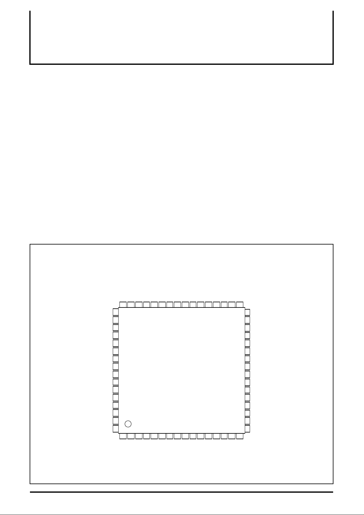
PIN CONFIGURATION (TOP VIEW)
APPLICATION
NTSC type color TV, projecter
RECOMMENDED OPERATING CONDITION
Recommended supply voltage.....................V3, 4, 21, 22, 23=4.75V
V5, 15, 16=8.0V
Supply voltage range........................V3, 4, 21, 22, 23=4.50 to 5.00V
V5, 15, 16 =7.6 to 8.8V
Maximum output current.............................................3.0mA (pin14)
4.0mA (pin13)
8.0mA (RGB output current)
3.0mA (AUDIO OUT output current)
AUDIO SW OUT
AUDIO IN
AUDIO OUT
FM DIRECT OUT
EXT AUDIO IN
VCO
VCO
VIDEO APC FILTER
VIDEO OUT
AFT OUT
RF AGC OUT
IF AGC FILTER
IF GND1
IF GND2
IF GND3
IF IN
GND
LIMITER IN
ABL
γ-CONT
COINCIDENCE
VIDEO SW OUT
SYNC SEP IN
TV/Y IN
Y SW OUT
VCD GND3
VCD GND2
VCD GND1
EXT/C IN
CHROMA APC FILTER
VIDEO SW IN
GND
41
46
454443
47
48
49
50
51
52
53
54
55
56
57
58
59
60
61
62
63
64
5
3
4
IF VCC2
6
H VCC
IIL VCC
1
GND
2
IF IN
CC1
IF V
403938
42
M52775FP
8
9
7
SCL
SDA
FBP IN
101112
H OUT
H OSC
37
363534
131415
V PULSE
FBP INV OUT
AFC 1 FILTER
CC1
Hi V
33
32
31
30
29
28
27
26
25
24
23
22
21
20
19
18
17
16
Hi VCC2
X-TAL 3.58
AUDIO BYPASS
FAST BLK
BLACK PEAK HOLD
R IN
AFC 2 FILTER
G IN
CONTRAST CONT
B IN
VCD V
CC3
VCD VCC2
VCD VCC1
B OUT
G OUT
R OUT
GND
Outline 64P6N-A
1
Page 2
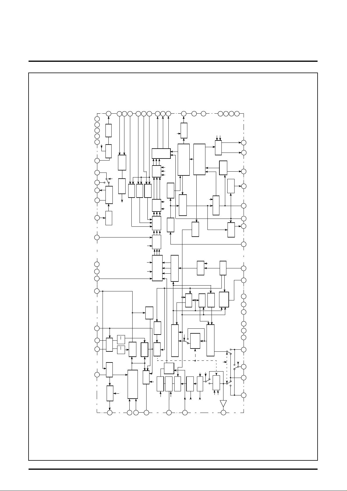
BLOCK DIAGRAM
MITSUBISHI ICs (TV)
M52775FP
VIF, SIF, VIDEO, CHROMA, DEFLECTION FOR NTSC
IF GND3
IF GND2
IF GND1
IF VCC1
IF VCC2
AUDIO IN
AUDIO SW OUT
EXT AUDIO IN
FM DIRECT OUT
AUDIO BYPASS
LIMITER IN
ABL
Hi VCC1
Hi VCC2
CONTRAST CONT
63
62
61
AUDIO ATT (7)
5049
52 53 4 3
31
47
46
16
25 1557
AUDIO OUT
SDA
9
51
AF
AMP
ATT
I / F
BUS
AUDIO SW
D/A
FM
DET
BUS
CONTROL
LIMITER
SCL
7
R IN
28
R EXT
INPUT
G IN
26
INPUT
G EXT
BRIGHT
SERVICE
COLOR
FAST BLK
B IN
24
30
INPUT
B EXT
(7)
SW
(7)
R OUT
18
CLAMP
AMP
DRIVE
RGB SW
BRIGHT
RGB
MATRIX
HV
B OUT
G OUT
20
19
BLK
RGB
CUT OFF (8)
V SYNC
RB
DRIVE (6)
SYNC
CONTRAST
V PULSE
14
V-PULSE
SERVICE SW
VERTICAL
COUNT DOWN
TRIG
EQ
ELIMINATE
SEP
CHROMA
DEMODULATOR
H VCC
IIL VCC
6
5
HORIZONTAL
COUNT DOWN
BGP
GENE
TINT
CONT
AFC GAIN
AFC-1
TINT
(7)
GND
GND
1
17
H-STOP
H-PHASE (4)
AFC-2
VCO
32FH
COINCI.
VCXO
GND
GND
48
33
H OUT
101112
AFC 2 FILTER
27
H OSC
FBP INV OUT
13
INV
AFC 1 FILTER
8
FBP IN
COINCIDENCE
44
DET
SYNC SEP IN
42
X-TAL 3.58
32
CHROMA APC FILTER
35
VIDEO OUT
VIDEO APC FILTER
VCO
VCO
IF AGC FILTER
56
55
54
60
44
ππ
+–
VCO
IF AGC
RF AGC
DELAY ADJ (6)
59
64
IF IN
RF AGC OUT
DET
VIDEO
VIF
AMP
2
IF IN
CONTRAST
(7)
DET
LOCK
APC
DET
AFT
58
AFT OUT
REF
FILTER
ADJ
DET
LIM (γ)
PEAK
MUTE
VIDEO
BLACK
STRETCH
DEFEAT
MUTE SW
29
BLACK PEAK HOLD
2ND AMP
CLAMP
ON/OFF
DET
KILLER
BPF SW
CHROMA
TONE
VIDEO
(6)
SHARPNESS
45
γ-CONT
Acc
DET
BPF/
TAKEOFF
Adj (2)
DL TIME
DELAY
DL Fine Adj
SW
TRAP
LIMIT
CHROMA
(Acc)
1ST AMP
CHROMA
TRAP Adj 1
DET
APC
CHROMA
BPF SW
TRAP
X2
TRAP Adj 2
40
Y SW OUT
VCD GND3
39
VCD GND2
38
VCD GND1
37
VCD VCC3
23
VCD VCC2
22
VCD VCC1
21
EXT/C IN
36
TV/EXT
VIDEO SW OUT
VIDEO SW IN
TV/Y IN
41 4334
2
Page 3
∗
°
°
±
VIF, SIF, VIDEO, CHROMA, DEFLECTION FOR NTSC
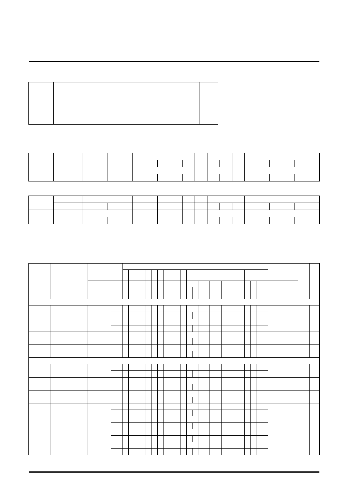
ABSOLUTE MAXIMUM RATINGS
Symbol Parameter Ratings Unit
V
CC
P
d
T
opr
T
stg
S
urge
2
I
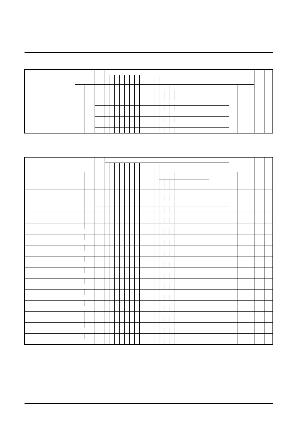
C BUS DEFAULT CONDITION OF ALL BLOCKS IN M52775FP
All
Blocks
Supply voltage 6.0, 9.0 V
Power dissipation 0.85 W
Operating temperature -20 to +65
Storage temperature -40 to +150
Electrostatic discharge
200 V
sub address 00H 01H 02H 03H 04H 05H 06H 07H
function DLA P/N
AVSW
DFA
TADJ2
TRAP
ATT
DATA 20H 00H 00H 40H 20H 20H 02H 40H
function 32 0 0 000064320322000064
C
C
SHARP
DEFE
CONT
MITSUBISHI ICs (TV)
M52775FP
TV/EXT
DLTA
Y/C black
HADJ
TINT
sub address 08H 09H 0AH 0BH 0CH 0DH 0EH 0FH 10H 12H 13H
All
Blocks
function
COLOR
HP BRI DR
DATA 20H 40H 20H 20H 20H 80H 80H 80H 00H 00H 00H
function 32 0 8 32 32 0 32 128 128 128 0000 000
MUTE
DB CR CG CB TRF
Please refer to the following sub-address data for each parameter you measure.
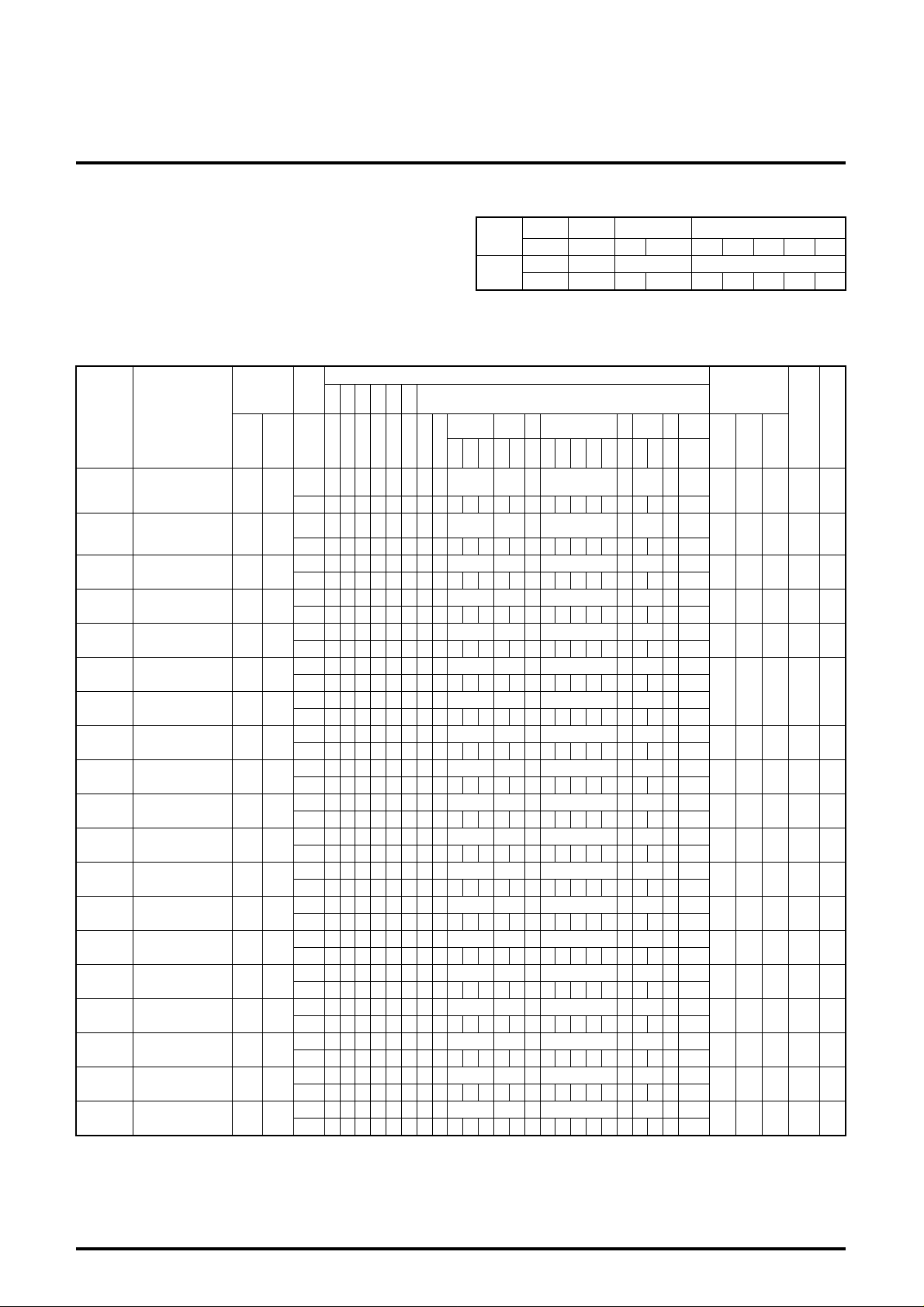
ELECTRICAL CHARACTERISTICS
Input signal SW
Symbol Parameter
Input SG PIN
Supply current
−
I
CC4
I
CC75
I
CC8a
I
CC8b
VIF block
−
Vdc
Vo
P/N Video S/N
f
V
Vin
min
Vin
max
Default conditions of
supply current
Pin3, 4, 21, 22, 23
supply current
Pin5
supply current
Pin 15, 16
supply current
Default conditions
of IF type
Video detection
output DC voltage
Video detection
output
Video frequency
characteristics
Input sensitivity
Maximum
permissible input
−−
−−
−−
−−
−−
−−
64
SG1
2
64
SG3
2
64
SG4
2
64
SG5
2
64
SG6
2
(Ta=25 ° C, pin3, 4, 21, 22, 23:4.75V supply/pin5, 15, 16:8V supply unless otherwise noted.)
Test conditions
S12S60S
45
P49P51P52P57P58P59P
60
SW 20H 20H 40H
PIN 32 0
SW
PIN
SW
PIN
SW
PIN
SW 1 1 1 20H 00H 00H 00H
PIN 32 0
SW
PIN M
SW 0
PIN M
SW 0
PIN M
SW 0
PIN M
SW 0
PIN M
SW 0
PIN M
DLAVC
Sub address function
00H 01H 03H 04H
AV
DEF-
ATT
S
OA
32 0
00
W
64
0
EAT
0
2WIND
V
P
P
3
9
4
4.75
8V 8V
V
MM
M
4.75
8V 8V
V
SER HST
CC
P
P
21
Min. Typ. Max.
15
22
16
23
−−−−
4.75
V
60 86 112 mA
23 33 43 mA
11 16 21 mA
M
−−−−
4.75
V
3.7 4.2 5.1 V
1.9 2.2 2.5 V
43 53 − dB
4.5 5.5 − MHz
− 43 50 dB µ
102 107 − dB
AFCG
Limits
Unit Note
3
Page 4
−
−
MITSUBISHI ICs (TV)
M52775FP
VIF, SIF, VIDEO, CHROMA, DEFLECTION FOR NTSC
−
−
−
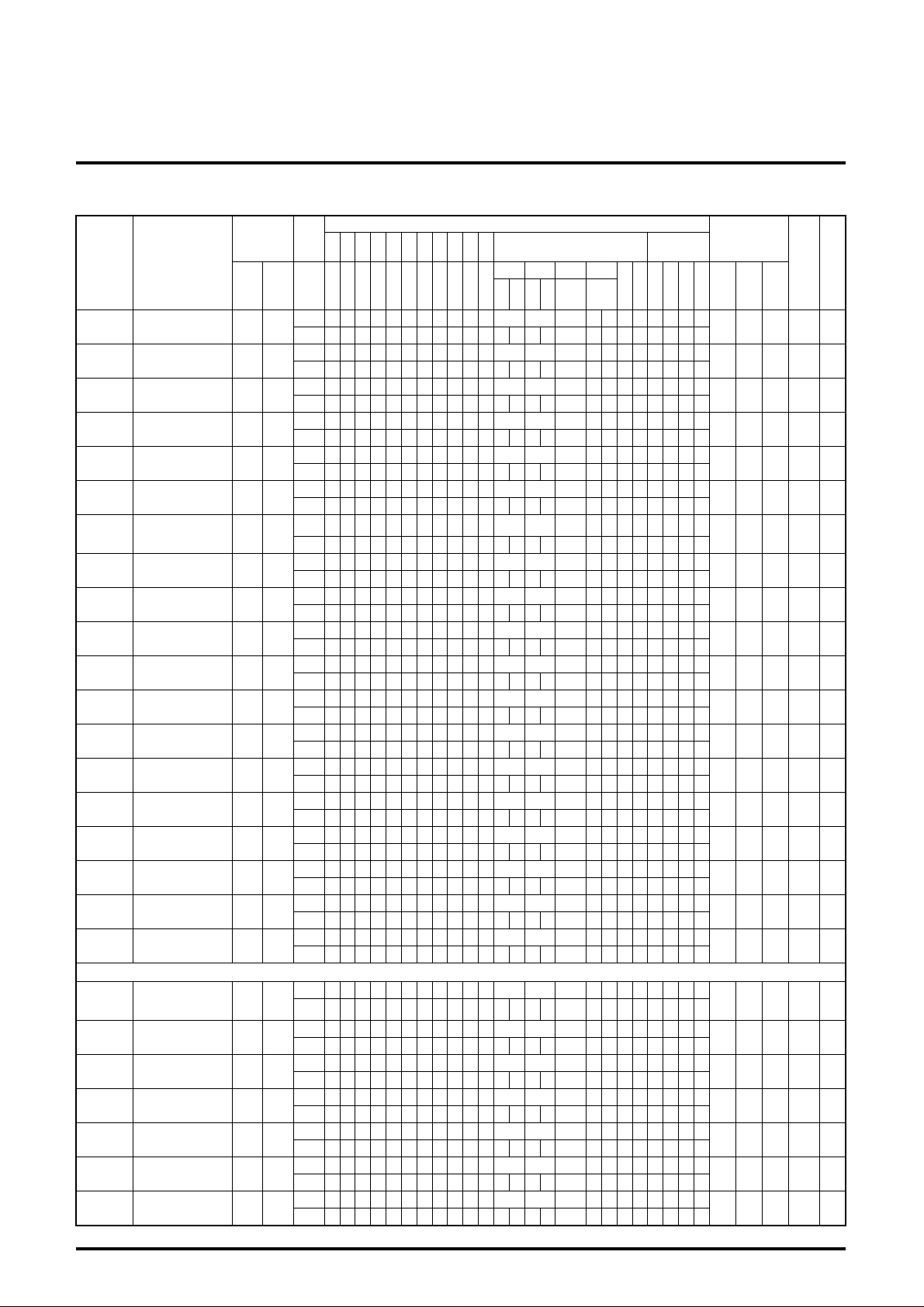
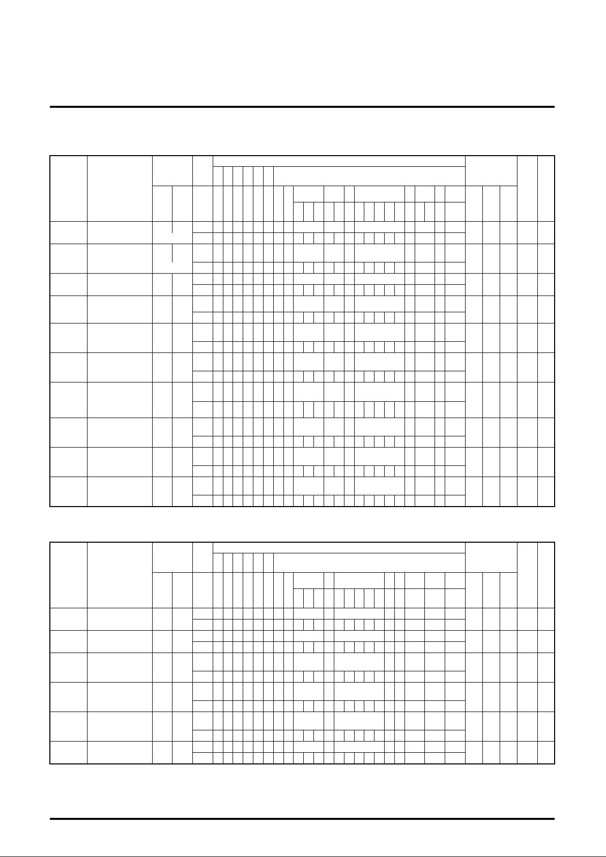
ELECTRICAL CHARACTERISTICS
Input signal SW
Symbol Parameter
Input SG PIN
GR
VIH
VIT
VIL
V58
uAFTN
V58H
V58L
V59H
V59L
CRU
CRL
CRT
AGC control
range
IF AGC
maximum voltage
IF AGC voltage
(80 dBu)
IF AGC
minimum voltage
AFT DEFEAT
voltage
AFT detection
sensitivity
AFT maximum
voltage
AFT minimum
voltage
RF AGC
maximum voltage
RF AGC
minimum voltage
Capture range
(upper)
Capture range
(lower)
Capture range
(total)
IM Inter modulation
DG DG
DP DP
SPN Sync ratio
DLPH
DLPL
Maximum delay
point
Minimum delay
point
SIF block
−
VAF
SIF type standard
condition
AF output DC
voltage
VoAF AF direct output 47
VoAF
max
ATT
THD
AF
LIM
AF maximum
output
Maximum
attenuation
AF output
distortion factor
Input limiting
sensitivity
−−
−−
64
2
64
2
−−
64
2
64
2
64
2
64
2
64
2
64
2
64
2
−−
64
2
64
2
64
2
64
2
64
2
64
2
−−
47
47
47
47
47
SW
PIN
SW 0
PIN M
SW 0
SG7
PIN M
SW 0
SG8
PIN M
SW 0
PIN M
SW
SG9
PIN M
SW 0
SG10
PIN M
SW 0
SG11
PIN M
SW 0 00H
SG3
PIN M 0
SW 0 3FH
SG3
PIN M 63
SW 0
SG9
PIN M
SW 0
SG9
PIN M
SW
PIN
SW 0
SG12
PIN M
SW 0
SG13
PIN M
SW 0
SG13
PIN M
SW 0
SG13
PIN M
SW 0 00H
SG14
PIN M 00
SW 0 3FH
SG15
PIN M 63
SW 0 20H 20H 40H
PIN 32
SW
SG17
PIN M
SW
SG16
PIN M
SW 7FH
SG16
PIN M 127
SW 00H
SG16
PIN M 0
SW
SG16
PIN M
SW
SG16
PIN M
(cont.)
S12S60S
45
P49P51P52P57P58P59P
Test conditions
Sub address function
00H 01H 03H 04H
AV
60
DLAVC
OA
DEF-
ATT
S
W
EAT
V
CC
P
P
P
3
15
9
4
16
Limits
P
21
Min. Typ. Max.
22
23
50 64 − dB µ
Unit Note
calcu-
late
3.8 4.2 4.6 V
2.4 2.8 3.2 V
1.6 2.0 2.4 V
3.7 4.0 4.3 V
52 74 96
V
8V 8V
4.75
V
6.5 7.0 − V
4.75
mV/
kHz
0.8 1.3 V
7.2 7.8 − V
0.2 0.8 V
0.7 1.0 − MHz
0.7 1.0 − MHz
1.4 2.0 − MHz
calcu-
late
30 35 − dB
2 7 %
2 7 deg
25.0 27.5 32.0 %
95 105 − dB µ
63 73 dB µ
V
8V 8V
4.75
V
0
64
4.75
−−−−
2.0 2.4 2.8 V
240 340 440
410 590 770
mVrms
mVrms
59 68 − dB
− 0.6 3 %
− 40 46 dB
4
Page 5
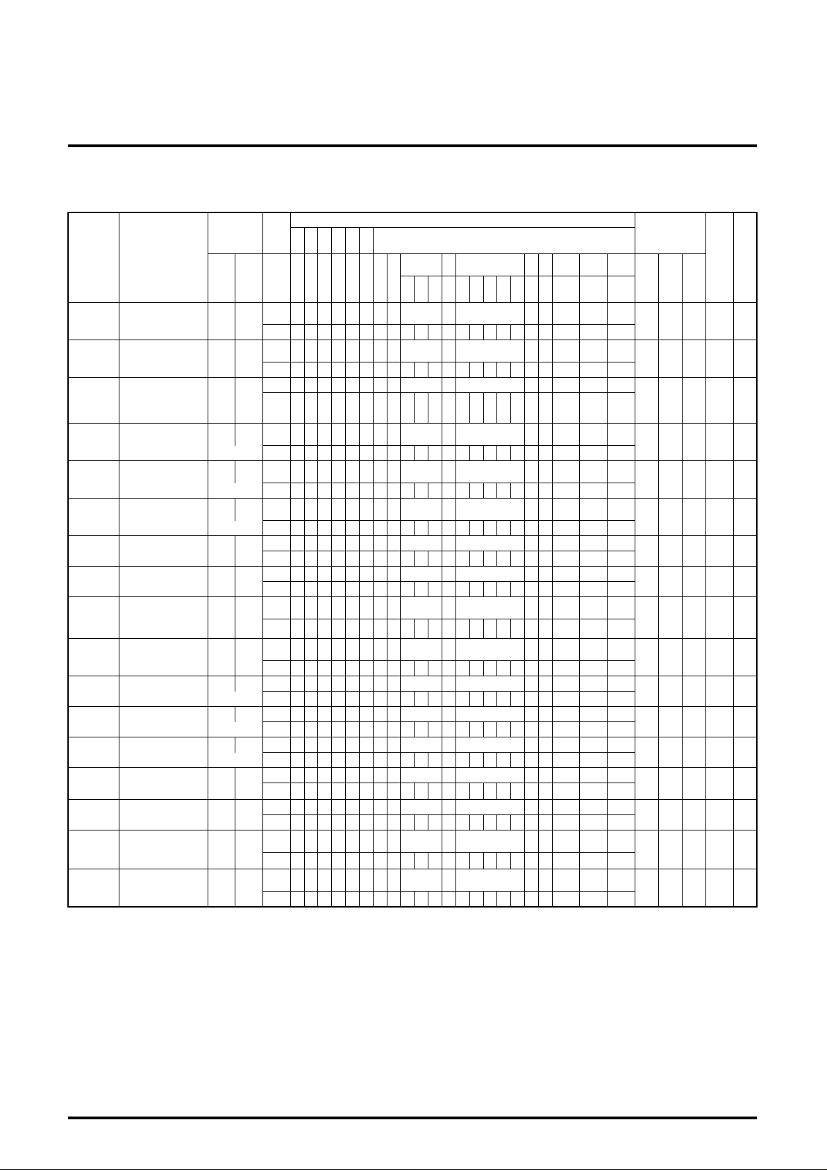
ELECTRICAL CHARACTERISTICS (cont.)
Input signal SW
Symbol Parameter
Input SG PIN
AMR AMR 47
AFSN AF S/N 47
GEAu EXT audio GAIN 53
SG20
SG17
SG22
S12S60S
45
P49P51P52P57P58P59P
SW
PIN M
SW
PIN M
SW 40H
PIN M 1
ELECTRICAL CHARACTERISTICS
chroma block (∗C0 to C13:input SGS at pin41 IN)
Symbol Parameter
−
Cn1
Cn2
A
CC1 ACC 1
CC2 ACC 2
A
Default conditions
of chroma
Output signal
amplitude 1
Output signal
amplitude 2
OV Chroma overload
VikP
killP
APC1
R/BP
θR-Y
P
CC
Threshold color
killer on
Residual color
leakage at killer on
APC Pull-in
range 1
Ratio of
(R-Y/B-Y)
Demoduration
phase θR-Y
Residual carrier
leakage
TC1 Tint control 1
TC2 Tint control 2
Input signal SW
Input SG PIN
−−
36 SS
36 SS
36 VS SW
v=+6dB PIN M
36 VS SW
v=-20dB PIN M
36 VS SW
eb=800mV PIN M
36 VS SW
v=variable PIN M
36 VS SW
v=-45dB PIN M
36 VS SW
f=variable PIN M
36 VS SW
eb=monochroma
36 VS SW
eb=monochroma
36 SS
36 VS SW 7FH
eb=monochroma
36 VS SW 00H
eb=monochroma
S12S60S
45
P12P18P19P
SW 1 1 1 02H 40H 40H
PIN 2 0 0 64 0 8 64 64
SW
PIN M
SW
PIN M
PIN M M
PIN M M
SW
PIN M
PIN M 127
PIN M 0
MITSUBISHI ICs (TV)
M52775FP
VIF, SIF, VIDEO, CHROMA, DEFLECTION FOR NTSC
Test conditions
Sub address function
00H 01H 03H 04H
AV
60
DLAVC
OA
DEF-
ATT
S
W
EAT
VCC
P
P
P
3
15
9
4
16
Test conditions
Sub address function
06H 07H 09H
20
TV/
DL
AU
EX
TINT
TA
TO
T
05H08H0
H
CONTCO
P
40H 40H 64H
VCC
P
BH
mu
L
100
P
P
3
15
V
5
4
16
te
4.75
8V 8V
V
Limits
P
21
Min. Typ. Max.
22
23
45 50 − dB
49 58 − dB
-2.0 0.0 2.0 dB
Limits
P
21
Min. Typ. Max.
22
23
−−−−
4.75
V
2000 2800 3600 mVP-P
1900 2700 3500 mVP-P
1 4 6 dB
-3 0 3 dB
-1 2 5 dB
− -41 -30 dB
0 40 150
+300 +800
-300 -1100
0.60 0.81 1.00 −
80 95 110 deg
0 60 120
30 44 60 deg
30 46 60 deg
−
−
Unit Note
Unit Note
mVP-P
f=eb
Hz
=ec
100kHz
100kHz
mVP-P
ec=
eb+
ec=
eb+
5
Page 6
MITSUBISHI ICs (TV)
M52775FP
VIF, SIF, VIDEO, CHROMA, DEFLECTION FOR NTSC
Sub
address
No.
function COLOR DR MUTE
DATA 00H 20H 00H
Y
0
function 0 32 0 0 0 0
ELECTRICAL CHARACTERISTICS
Video & RGB I/F block (∗ input SGS at pin42 IN. VCC:P3, P4, P21, P22, P23=4.75V. P5, P15, P16=8.0V supply)
02H
TRF2TR
DF
A
Test conditions
Sub address function
05
04H
H
SH
DEFPCO
AR
AP
0/1
NT
P
40
H
7F
H
127
Input signal SW
Symbol Parameter
Input SG PIN
−
Ymax
Default conditions of
video & RGB I/F
Maximum video
amplitude
−−
34 SGA
GY Video gain 34 SGA
FBY
2AGY
CTR1
TRF1
YSW
YSmax
E→T
CT
T→E
CT
Video frequency
characteristics
Double amplifier
standard output
Chroma trap
attenuation 1
Chroma trap fine
adj. attenuation 1
Y SW OUT
standard output
Y SW OUT
maximum output
EXT→TV
crosstalk
TV→EXT
crosstalk
34 SGB
34 SGA
34 SGF
34 SGF
SGB
34
V=0.71
VP-P
SGB
34
V=
1.5VP-P
SGB
36
f=5MHz
SGB
34
f=5MHz
YDL1 Y delay time 1 34 SGA
YDL2 Y delay time 2 34 SGA
YDL3 Y delay time 3 34 SGA
GTnor Video tone 1 34 SGB
GTmax Video tone 2 34 SGB
GTmin Video tone 3 34 SGB
GT2M Video tone 4 34 SGB
GT5M Video tone 5 34 SGB
S12S60S
45
P18P19P20P25P40P43P45P
46
SW 1 1 1 00H 20H
PIN 00032064201006432
SW
PIN M M M
SW
PIN M M M
SW
PIN M
SW 20H
PIN M 32
SW 00/20H 20H
PIN M M M
SW 20/30H 20H
PIN M M M 0/1 132
SW
PIN M
SW
PIN M
SW 0EH/0AH
PIN M
SW 0AH/0EH
PIN M
SW 08H
PIN M M M 0
SW 09H
PIN M M M 1
SW
PIN M M M
SW
PIN M M M
SW 3FH
PIN M M M 63 0
SW 00H
PIN M M M 0 0
SW
PIN M M M
SW
PIN M M M
08H 0BH 13H
H
I
H
0BH
MU
DR
TE
20H
032 96
0
0
32
0 0/1
0C
10H
H
DB
TRF
20
60H
H
00/60H
DL
TA
06H
TV/
Y/CBlackHADJBR
EX
T
02H
1/0
0/1
0A
40
Min. Typ. Max.
2.5 3.5 4.5 VP-P
5 8 11 dB
-1 2 5 dB
1.6 2.1 2.6 V
0.51 0.71 0.91 V
1.0 1.4 1.8 V
200 280 360 nsec
150 200 250 nsec
210 300 390 nsec
1.5 2.1 2.7 V
-1.3 2.2 5.7 dB
-12 -8 -4 dB
-1.8 1.2 4.2 dB
-7 -3.5 0 dB
SER HST AFCG
Limits
Unit Note
−
−
-18 dB
− -50 -40 dB
-45 -35 dB
−
P-P
P-P
P-P
P-P
6
Page 7
ELECTRICAL CHARACTERISTICS
Video & RGB I/F block (cont.)
Input signal SW
Symbol Parameter
Input SG PIN
GYnor Contrast 1
GYmin Contrast 2
Lumnor Bright 1
Lummax Bright 2
Lummin Bright 3
D (R) Drive R 34 SGA
D (B) Drive B 34 SGA
EX (R) EXT (R) I/O
EX (G) EXT (G) I/O
EX (B) EXT (B) I/O
34 SGB SW
f=100kHz PIN M M M
34 SGB SW
f=100kHz PIN M M M 0
−−
−−
−−
SW
PIN M M M
SW
PIN M M M
SW
PIN M M M 0
SW
PIN M 0/63
SW
PIN
SGD
SGD
SGD
SW
PIN M
SW
PIN M
SW
PIN M
30
28
30
26
30
24
S12S60S
45
P18P19P20P25P40P43P45P
M
MITSUBISHI ICs (TV)
M52775FP
VIF, SIF, VIDEO, CHROMA, DEFLECTION FOR NTSC
46
Test conditions
02H 04H
TRF2TR
DF
A
AP
Sub address function
05
H
SH
AR
P
DEFPCO
TV/
DL
EX
NT
TA
T
00
H
7F
H
127
7F
H
127
7F
H
127
06H
Y/CBlackHADJBR
0A
00
00
0C
0BH
10H
H
7F
H
127
H
D
MU
DB
I
TRF
TE
R
H
00/
3FH
00/
3F
H
0/
63
H
0
00
H
0
00
H
0
Limits
Unit Note
Min. Typ. Max.
1.1 1.6 2.1 V
− 20 100 mV
2.2 2.6 3.0 V
0.7 1.0 1.3 V
-1.3 -1.0 -0.7 V
3.5 5.5 7.5 dB
3.5 5.5 7.5 dB
3.5 4.3 5.1 V
3.5 4.3 5.1 V
3.5 4.3 5.1 V
P-P
P-P
P-P
P-P
Video & RGB I/F block (cont.)
Input signal SW
Symbol Parameter
Input SG PIN
OFRG
OFBG
C (R) Cut off R
C (G) Cut off G
C (B) Cut off B
DLF
Offset voltage
R-G
Offset voltage
B-G
DL fine delay
amount
−−
−−
−−
−−
−−
34
SGA
Test conditions
S12S60S
45
P18P19P20P25P40P43P45P
02H
46
DF
A
TRF2TR
05
H
CO
NT
AP
Sub address function
Y/CBlackHA
08H0A
CO
LO
DJ
R
06H
TV/
DL
EX
TA
T
0DH
H
BR
CR CG CB
I
0EH 0FH
SW
PIN M
SW
PIN M M
SW
00/
FFH
PIN M 0/255
SW
00/
FFH
PIN M 0/255
SW
00/
FFH
PIN M 0/255
SW 02/00H
PIN M M M
1/0
Limits
Unit Note
Min. Typ. Max.
-120 0 120 mV
-120 0 120 mV
1.2 1.5 1.8 V
1.2 1.5 1.8 V
1.2 1.5 1.8 V
20 45 70 nsec
7
Page 8
ELECTRICAL CHARACTERISTICS
Video & RGB I/F block (cont.)
Input signal SW
Symbol Parameter
Input SG PIN
Ccon1 Color control 1 36 SGE
Ccon2 Color control 2 36 SGE
VMF Video mute 34
MTXB Matrix 1
MTXG Matrix 2
MTXR Matrix 3
OSD1 OSD speed 1
OSD2 OSD speed 2
36 VS SW 02H
ec=eb+100kHz
36 VS SW 02H
ec=eb+100kHz
36 VS SW 02H
ec=eb+100kHz
24,26
28,30
24,26
28,30
GYmax1 Contrast 3 34 SGA
GYmin1 Contrast 4 34 SGA
BLS1
BLS2
BLS3
ABL1
ABL2
γ1
γ2
Black expansion
characteristics 1
Black expansion
characteristics 2
Black expansion
characteristics 3
ABL
characteristics 1
ABL
characteristics 2
Gamma
characteristics 1
Gamma
characteristics 2
34 SGC SW 0AH/1AH
V=0.2VP-P PIN M
34 SGC SW 0AH/1AH
V=0.45VP-P PIN M
34 SGC SW 0AH/1AH
V=0VP-P PIN M
−−
−−
34 SGA
34 SGA
SW 02H
PIN M 0
SW 02H
PIN M 0
SW
SGB
f=
PIN M M M
3.58M
PIN M 0 64
PIN M 0 64
PIN M 0 64
SW
SGD
PIN M M M
SW
SGD
PIN M M M
SW
PIN
SW
PIN M M M
SW
PIN
SW
PIN M
SW
PIN
SW
PIN M
S12S60S
45
P18P19P20P25P40P43P45P
MMM
2.9
V
0V
M
M
4.75
V
1V
MITSUBISHI ICs (TV)
M52775FP
VIF, SIF, VIDEO, CHROMA, DEFLECTION FOR NTSC
Test conditions
Sub address function
05
02H
46
TRF2TR
DF
A
AP
4.75
V
0V
06H
H
TV/
DL
CO
EX
NT
TA
T
7F
H
127
7F
H
127
7F
H
127
7F
H
127
Y/CBlackHA
0/1
0/1
0/1
08H0A
0DH
0EH 0FH
H
CO
BR
LO
R
7FH48
127
7FH48
127
40H64
40H64
40H64
I
H
72
H
72
H
100
H
100
H
100
CR CG CB
DJ
Limits
Unit Note
Min. Typ. Max.
1.0 1.6 2.2
− 30 100
mVP-P
mVP-P
− -45 -35 dB
1.8 2.6 3.4 VP-P
0.7 1.0 1.3 VP-P
1.4 2.0 2.6 VP-P
− 20 100 nsec
− 50 130 nsec
2.0 2.8 3.6 VP-P
− 20 100
100 250 850
-100 50 200
-100 0 100
mVP-P
mVP-P
mVP-P
mVP-P
3.35 3.75 4.15 V
1.05 1.55 2.05 V
2.6 3.5 4.4 VP-P
2.0 2.7 3.4 VP-P
0BH
00/
40H
MUTE
:0/1
8
Page 9
MITSUBISHI ICs (TV)
M52775FP
VIF, SIF, VIDEO, CHROMA, DEFLECTION FOR NTSC
ELECTRICAL CHARACTERISTICS
Synchronization/Deflection Block
Input signal SW
Symbol Parameter
Input SG PIN
Default conditions
−
ISS
BGP1
BGP2
BGPW
fH
FPH1
FPH2
HPT1
HPT2
HPT3
TH
VH
HSTO
of synchronization
deflection
Sync. sep. input
sensitivity; current
Burst gate pulse
timing 1
Burst gate pulse
timing 2
Burst gate
pulse width
Horizontal free
run frequency
Horizontal pull-in
range 1
Horizontal pull-in
range 2
Horizontal pulse
timing 1
Horizontal pulse
timing 2
Horizontal pulse
timing 3
Horizontal pulse
width
Horizontal pulse
amplitude
Horizontal pulse
stop function
−−
−−
SY SGa
SY SGb
SY SGa
−−
SY
SY
SY SGa
SY SGa
SY SGa
−−
−−
−−
AFCG AFG gain SY SGa
fV
SW Service switch
FPV
VW
Vertical free run
frequency
Vertical pull-in
range
Vertical pulse
width
−−
−−
SY
−−
SW 11 00
PIN 8 0 0 0 0
SW
PIN M
SW
PIN M M
SW
PIN M M
SW
PIN M
SW
PIN M
SW
SGc
f=vari-
PIN M M
able
SW
SGc
f=vari-
PIN M M
able
SW
PIN M M
SW
PIN M M 0
SW
PIN M M 15
SW
PIN M
SW
PIN M
SW 10H
PIN M 1
SW 0 00/20H
PIN M
SW
PIN M
SW 00H/08H
PIN M
SW
SGd
f=vari-
PIN M
able
SW
PIN M
S12S
60
P8P10P16P12P13P14P18P19P20P
Test conditions
09
H
42
H
P
40
H
00
H
78
H
No.
Sub address function
12
13H
H
SU
B
SERHSTAF
VP
O
00
00H
H
0/1
Sub
address
function DLTA
DATA 20H 00H
D
0
function 0 0 1 0
VCC
P
P
3
15
5
4
CG
16
4.75
8V 8V
V
06H 08H
TV/
EXT
Limits
P
P
21
Min. Typ. Max.
22
23
−−−−
4.75
V
− 0.1 0.2 mA
3.5 4.5 5.5 µsec
3.5 4.5 5.5 µsec
4.8 6.0 7.2 µsec
15.3 15.7 16.1 kHz
+350 +600
− -800 -350 Hz
7.2 8.3 9.4 µsec
-2.6 -2.0 -1.4 µsec
1.2 1.7 2.2 µsec
6.7
21 25 29 µsec
3 3.7 − V
− 0.2 0.5 V
0/1
4.75
8V 8V
V
2.0 3.7 10 dB
51 54 57 Hz
4.75
V
− 0 0.5 V
−
−
0.35 0.52 0.65 msec
AUTO COLOR
Unit Note
− Hz
67 Hz
9
Page 10
ELECTRICAL CHARACTERISTICS
Synchronization/Deflection Block (cont.)
Symbol Parameter
VBLKW
Vertical blanking
width
Vertical sync.
WVSS
detection
minimum width
FBPI FBP inv OUT
Input signal SW
Input SG PIN
−−
SY SGd SW
f60Hz width
variable
S12S
60
P8P10P16P12P13P14P18P19P20P
SW
PIN M M M
PIN M
SW 4.65 4.75 4.85
PIN
MITSUBISHI ICs (TV)
M52775FP
VIF, SIF, VIDEO, CHROMA, DEFLECTION FOR NTSC
Test conditions
Sub address function
09
H
42
H
P
10H
V-POTR
11H12
V
HA
F
SIZ
13H
H
SU
B
SERHSTAF
VP
O
CG
VCC
P
P
P
3
15
5
4
16
M
Limits
P
21
Min. Typ. Max.
22
23
0.9 1.1 1.3 msec
9.5 12.5 −µsec
0 0.5
−
Unit Note
H
V
L
10
Page 11
MITSUBISHI ICs (TV)
M52775FP
VIF, SIF, VIDEO, CHROMA, DEFLECTION FOR NTSC
ELECTRICAL CHARACTERISTICS TEST METHOD
P/N Video S/N
1. Input SG3 and measure the rms value of output signal at pin 57.
2. P/N is defined as follows:
V
P/N=20log
0NEG measured value (VP-P) ×10
Measured value (mVrms)
Vf Video frequency characteristics
1. Input SG4 and set the frequency f2 to 44.75MHz so that the beat
element of 1MHz is output to pin 57.
2. Then set the applied voltage at pin 60 so that the beat element of
1MHz at pin 57 may be 100dBµ.
3. Decrease f2 to the level at which the beat element becomes 3dB
smaller than the element of 1MHz, and read the value at that
level.
P57
100dBµ
1MHz BW
Vin min. Input sensitivity
1. Decrease SG5 level until the video detector output is 3dB
smaller then the measured value of Parameter V3 “Video
detector output”.
Vin max. Maximum permissible input
1. Input 90dBµ SG6.
2. V
A is the output level at pin 57. Increase SG6 voltage until the
output at pin 57 becomes 3dB smaller than VA. The input levell at
that time is the maximum permissible input.
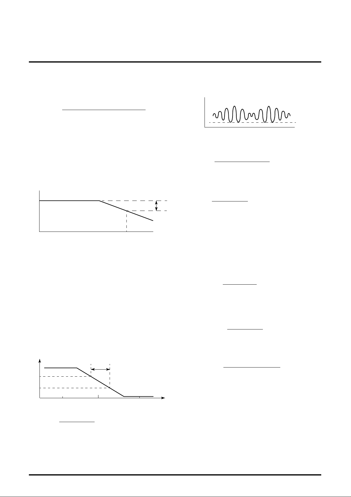
µAFTN AFT detector sensitivity
V58H Maximum AFT voltage, V58L Minimum AFT voltage
See the following figure.
P1
5.0V
V1HN
∆f
3
×0.7
(dB)
3dB
IM Intermodulation
1. Adjust the applied voltage at pin 60 so that the lowest output
signal voltage at pin 57 is 2.2V.
P57
2.2V
2. Measure elements of 0.92MHz and 3.579545MHz of output at
pin 57.
3. IM is defined as follows:
IM=20log
Element of 0.92MHz
Element of 3.579545MHz
(dB)
ATT Maximum attenuation
1. Measure the element of 400Hz of output at pin 51.
ATT=20log
2.
V
Measured value
(dB)
0AFmax
LIM Input limiting sensitivity
Decrease the input level of SG18. Measure the input level when the
element of 400Hz at pin 52 is 3dB smaller than V
0AFM (S6:
Maximum AF output (6.0M)).
AMR
1. Vam is the element of 400Hz at pin 52.
2. AMR is defined as follows:
0AF (mVrms)
AMR=20log
V
Vam (mVrms)
(dB)
AF S/N
1. Measure the noise (20Hz to 100kHz) of output at pin 52.
2. AF S/N is defined as follows:
AF S/N=20log
0AFmax
Measured value
(dB)
V
GEAu EXT Audio GAIN
Input SG22 at pin 53, and measure the output V
GAIN=20log
Input signal VP-P
Output signal VP-P (pin49)
P-P at pin 49.
(dB)
3.0V
44.75Mz 46.75MHzf0
µAFTN is defined as follows:
µAFTN=
(5.0-3.0)×103mV
∆f kHz
11
(mV/kHz)
V1LN
Cn1 Output signal amplitude 1
Cn2 Output signal amplitude 2
f
1. Input SS from pin 36 IN.
2. Measure output amplitude, Cn1 and Cn2, at pins 18 and 20
respectively.
Page 12

MITSUBISHI ICs (TV)
M52775FP
VIF, SIF, VIDEO, CHROMA, DEFLECTION FOR NTSC
ACC1
1. Input VS (eb=570mV:level+6dB) from pin 36 IN.
2. Measure the output amplitude at pin 20.
3. ACC1 is defined as follows:
A
CC1=20log
CC2
A
Measured value (V
Cn1 (VP-P)
P-P)
(dB)
1. Input VS (input level:-20dB) from pin 36 IN.
2. Measure the output amplitude at pin 20.
CC2 is defined as follows:
3. A
A
CC2=20log
Measured value (V
Cn1 (VP-P)
P-P)
(dB)
OV Chroma overload
1. Input VS (ec=800mV
P-P:chroma+3dB) from pin 36 IN.
2. Measure the output amplitude at pin 20.
3. OL is defined as follows:
OL=20log
Measured value (V
Cn1 (VP-P)
P-P)
(dB)
VikP Threshold color killer on
1. Input VS (level:variable) from pin 36 IN at input level 0dB.
2. Lower the input level whth monitoring the output amplitude at pin
20 and measure the input level when output amplitude isnot
found.
KillP Residual color leakage at killer on
1. Input VS (level:-45dB) from pin 36 IN.
2. Measure the output amplitude at pin 20.
APC1 APC pull-in range 1
1. Input VS (f=eb=ec=variable) from pin 36 IN.
2. Change the input signal frequency and measure the frequency
range from the point at which signal is output to pin 20 and to the
point that no signal is output to the pin. The reference value is
3.579545MHz.
R/B P Ratio of (R-Y/B-Y)
1. Input VS (eb=single chroma=ec+100kHz) from pin 36 IN.
2. V20 is the output amplitude at pin 20.
3. V18 is the output amplitude at pin 18.
4. R/B P is defined as follows:
R/B P=20log
V18 (VP-P)
V20 (VP-P)
(dB)
θR-Y P Demodulation phase
1. Input VS (ed=single chroma=ec+100kHz) from pin 36 IN.
2. V20 is the output amplitude at pin 20.
3. V18 is the output amplitude at pin 18.
4. R-YP is defined as follows:
V18×3.8
θR-Y P=tan
-1
(V20×1.9)+45°
(deg)
CC Residual carrier leakage
Measure the element of 3.58MHz of the demodulated output in noinput state.
TC1 Tint control 1, TC2 Tint control 2
1. Input VS (see the following figure) from pin 36 IN. Based on the
output voltage at pin 20, find the absolute angle as shown in the
following figure.
-180°
A
0° 90°
90°
A
B
θ
θ=tan
-1
(B/A)
B
GND
0°
12
Page 13

MITSUBISHI ICs (TV)
M52775FP
VIF, SIF, VIDEO, CHROMA, DEFLECTION FOR NTSC
Ymax Maximum video output
1. Input SGA into pin 34 IN and input SGS from pin 42 IN.
2. Measure the amplitude (P-P) except that at blanking part of
output at pins 18, 19 and 20.
M
GY Video gain
1. Input SGA into pin 34 IN and input SGS from pin 42 IN.
2. Measure the amplitude (
P-P) except that at blanking part of
output at pins 18, 19 and 20. This amplitude is defined as G1.
M =G1
3. GY is defined as follows:
GY=20 log (G1V
P-P/0.714VP-P) (dB)
BW Video frequency characteristics
1. Input SGB (5MHz, 0.4VP-P) into pin 34 IN and input SGS from
pin 42 IN.
2. Measure the amplitude (P-P) except that at blanking part of the
output at pin 19. The amplitude is defined as YB.
3. BW is defined as follow:
BW=20 log (YB VP-P /GY VP-P) (dB)
2AGY Double amplifier standard output
1. Input SGA into pin 34 IN and input SGS from pin 42 IN.
2. Measure the amplitude (P-P) at pin 40 output.
CTR1 Chroma trap attenuation 1 (common to R/G/B output)
1. Input SS from pin 41 IN and input SGS into pin 42 IN. Measure
the frequency level of 3.58MHz at trap data 0. The level is
defined as N
0.
2. Then, measure the level at trap data 1.
3. CTR1 is defined as follows.
CTR1=20log
Measured value (mVP-P)
N0 (mVP-P)
(dB)
3. TRF1 is defined as follows.
TRF1=20log
TRFon (mVP-P)
N0 (mVP-P)
(dB)
4. Measure the most attenuation part in three condition of (2), and
the most attenuation part is defined as Y6.
The three condition of (2) is shown below.
TRAP FINE ADT SW FINE 2
condition 1 ON OFF
condition 2 OFF ON
condition 3 ON ON
YSW Y SW OUT standard output
1. Input SGB from pin 34 IN and input SGS into pin 42 IN.
2. Measure the output amplitude of the pin 43 output video block.
YSmax Y SW OUT standard output
1. Input SGB (video amplitude 1.5V
P-P) from pin 34 IN and input
SGS into pin 42 IN.
2. Measure the output amplitude of the pin 43 output video block.
E→T CT EXT→TV crosstalk
1. Input SGB (f=5MHz) from pin 36 IN and input SGS into pin 42 IN.
2. Specify pin 43 output for EXT to be VEXT.
3. Specify pin 43 output for TV to be VTV.
4. E→T CT is defined as follows.
E→T CT=20log
VTV (mV
VEXT (mVP-P)
P-P)
(dB)
T→E CT TV→EXT crosstalk
1. Input SGB (f=5MHz) from pin 41 IN and input SGS into pin 42 IN.
2. Specify pin 43 output for TV to be VTV.
3. Specify pin 43 output for EXT to be VEXT.
4. T→E CT is defined as follows.
T→E CT=20log
VEXT (mV
VTV (mVP-P)
P-P)
(dB)
YDL1 Y delay time1
1. Input SGA from pin 34 IN and input SGS into pin 42 IN.
2. Measure the delay time from signal input to output at pins 18, 19
and 20.
SGA Output signal
Measure the delay time
at the center point of rise.
M
TRF1 Chroma trap fine adj. attenuation 1
(common to R/G/B output)
1. Input SS from pin 34 IN and input SGS from pin 42 IN.
2. Measure the output amplitude of the element of 3.58MHz when
trap fine adj. switch is on. (TRFon)
13
YDL2 to 3 Y delay time2 to 3
1. Input SGA from pin 34 IN and input SGS into pin 42 IN.
2. Measure the delay time from signal output at pins 18, 19 and 20
to Y11, YDL1.
Page 14

MITSUBISHI ICs (TV)
GND
Output
M
waveform
M52775FP
VIF, SIF, VIDEO, CHROMA, DEFLECTION FOR NTSC
GTnor Video tone 1
1. Input SGB (f=3MHz) from pin 34 IN and input SGS into pin 42 IN.
2. Measure output amplitude at pins 18, 19 and 20.
GTmax Video tone 2
1. Input SGB (f=3MHz) from pin 34 IN and input SGS into pin 42 IN.
2. Measure output amplitude at pins 18, 19 and 20.
3. GTmax is defined as follows:
GTmax=20log
Measured value (V
GTnor (VP-P)
P-P)
(dB)
GTmin Video tone 3
1. Input SGB (f=3MHz) from pin 34 IN and input SGS into pin 42 IN.
2. Measure output amplitude at pins 18, 19 and 20.
3. GTmin is defined as follows:
GTmin=20log
Measured value (V
GTnor (VP-P)
P-P)
(dB)
GT2M Video tone 4
1. Input SGB (f=2MHz) from pin 34 IN and input SGS into pin 42 IN.
2. Measure output amplitude at pins 18, 19 and 20.
3. GT2M is defined as follows:
GT2M=20log
Measured value (V
GTnor (VP-P)
P-P)
(dB)
GT5M Video tone 5
1. Input SGB (f=5MHz) from pin 34 IN and input SGS into pin 42 IN.
2. Measure output amplitude at pins 18, 19 and 20.
3. GT5M is defined as follows:
GT5M=20log
Measured value (V
GTnor (VP-P)
P-P)
(dB)
GYnor Contrast 1
1. Input SGB (f=100kHz) from pin 34 IN and input SGS into pin 42
IN.
2. Measure output amplitude at pins 18, 19 and 20.
2. Measure DC voltage of output at pins 18, 19 and 20 except that
at blanking part.
3. Y22=(Lum max)-(Lum nor), Y23=(Lum min)-(Lum nor)
D (R) Drive R
1. Input SGA from pin 34 IN and input SGS into pin 42 IN.
2. Measure DRmin and DRmax which are output amplitude at pins
18 at D (R) data min and D (R) data max respectively.
3. D (R) is defined as follows:
D (R)=20log
DRmax (VP-P)
DRmin (VP-P)
(dB)
D (B) Drive B
1. Input SGA from pin 34 IN and input SGS into pin 42 IN.
2. Measure DBmin and DBmax which are output amplitude at pin
20 at D (B) data min and D (B) data max respectively.
3. D (B) is defined as follows:
D (B)=20log
DBmax (V
DBmin (VP-P)
P-P)
(dB)
EX (R) EXT (R) I/O, EX (G) EXT (G) I/O, EX (B) EXT (B) I/O
1. Input SGD into each of pin 30, 24, 26 and 28 and input SGS
into pin 42 IN.
2. Measure output amplitude which is higher than the pedestal level
at pins 18, 19 and 20. The amplitude at blanking part should not
be measured.
M
GYmin Contrast 2
1. Input SGB (f=100kHz) from pin 34 IN and input SGS into pin 42
IN.
2. Measure output amplitude at pins 18, 19 and 20.
3. GYmin is defined as follows:
GYmin=20log
Measured value (VP-P)
GYnor (VP-P)
(dB)
Lum nor Brightness control 1, Lum max Brightness control 2,
Lum min Brightness control 3
1. No signal is input. (Only SGS is input to pin 42 IN.)
OFRG Offset voltage R-G, OFBG Offset voltage B-G
1. Measure DC voltage of output at pin 18, 19 and 20 except that at
blanking part .
2. OFRG and OFBG are defines as follows:
OFRG=
(pin 18 Measured voltage)-(pin 19 Measured voltage) (mV)
OFBG=
(pin 20 Measured voltage)-(pin 19 Measured voltage) (mV)
14
Page 15

MITSUBISHI ICs (TV)
OSD1
OSD2
90%
10%
Output waveform at
pins18, 19 and 20.
M
M
M52775FP
VIF, SIF, VIDEO, CHROMA, DEFLECTION FOR NTSC
R (C) Cutoff R, G (C) Cutoff G, B (C) Cutoff B
1. Measure DC voltage of output at pin 18, 19 and 20 when R (C),
G (C) and B (C) data are maximum and minimum respectively.
The DC voltage at blanking part should not be measured.
2. R (C), G (C) and B (C) are defined as follows:
R (C), G (C) and B (C)=
(Voltage at data max.)-(Voltage at data min.) (V)
DLF Y delay time 〈fine〉
1. Input SGA from pin 34 IN and input SGS into pin 42 IN.
2. Measure the time lag (absolute value) between signal YDL3 and
output signal at pins 18, 19 and 20.
Y13
YDL3 signal
Measure the time lag
at the center point of rise.
Output signal
M
Ccon1 Color control 1, Ccon2 Color control 2
1. Input VS (ec=eb+100kHz) from pin 36 and input SGS into pin 42
IN.
2. Measure output amplitude at pins 18, 19 and 20 under each
condition.
VMF Video mute
1. Input SGF from pin 34 and input SGS into pin 42 IN.
2. Measure output amplitude of the element of 3.58MHz when the
mute switch is on and off. (VMFon, VMFoff)
3. VMF is defined as follows:
VMF=20log
VMFon (VP-P)
VMFoff (VP-P)
(dB)
MTXB Matrix 1, MTXG Matrix 2
1. Input VS (ec=eb+100kHz) from pin 36 and input SGS into pin 42
IN.
2. Measure output amplitude at pins 20 and 19.
(P20=MTXB, P19=MTXG)
MTXR Matrix 3
1. Input VS (ec=eb+100kHz) from pin 36 and input SGS into pin 42
IN.
2. Measure output amplitude at pin 18.
(P18=MTXR)
OSD1 OSD speed 1, OSD2 OSD speed 2
1. Input SGD into each of pin 30, 24, 26 and 28 and input SGS into
pin 42 IN.
2. Measure rise time and fall time of the signal of output at pins 18,
19 and 20. Measurement points should be higher than the
pedestal level and blanking part should not be measured.
GYmax1 Contrast 3, GYmin1 Contrast 4
1. Input SGA from pin 34 IN and input SGS into pin 42 IN.
2. Measure output amplitude at pina 18, 19 and 20 when 2.9V and
0V are extemally applied to pin 25.
ABR Bright increase voltage
1. Non-input.
2. Measure the voltage except for pin 19 blanking.
BLS1 Black expansion characteristics 1,
BLS2 Black expansion characteristics 2,
BLS3 Black expansion characteristics 3
1. Input SGC (BLS1=0.2V
P-P, BLS2=0.45VP-P, BLS1=0VP-P) from
pin 34 IN and input SGS into pin 42 IN.
2. With black expansion set to ON/OFF, specify the pin 19 output
voltages to be VBLSON1 to 3/BVLSOFF1 to 3, respectively.
3. The standard shall be expressed by BLS1 to 3=VBLSOFF1 to 3BVLSON1 to 3 (mVP-P).
ABL1 ABL characteristics 1, ABL2 ABL characteristics 2
1. Non-input.
2. When a voltage of 4.75V is applied to pin 46, measure the output
voltage at pin 19 and specify the value to be ABL1.
3. When a voltage of 0V is applied to pin 46, measure the output
voltage at pin 19 and specify the value to be ABL2.
γ1 Gamma characteristics 1, γ2 Gamma characteristics 2
1. Input SGA from pin 34 IN and input SGS into pin 42 IN.
2. When a voltage of 4.75V is applied to pin 45, measure the
amplitude of pin 19 output and specify the value to be γ1.
3. When a voltage of 0V is applied to pin 45, measure the
amplitude of pin 19 output and specify the value to be γ2.
4. γ1, γ2 are defined as follows:
γ2=γ1-Measured value (mV
P-P)
ISS Sync separation input sensitivity current
When current flows from pin 42, measure the flow current with the
burst gate pulse of P8SCP eliminated.
15
Page 16

MITSUBISHI ICs (TV)
Measure the output pulse width
at pin 14.
GND
Output waveform at
pins 18, 19 and 20
M
P13 waveform
GND
Hi
Lo
M52775FP
VIF, SIF, VIDEO, CHROMA, DEFLECTION FOR NTSC
BGP1 Burst gate pulse timing 1
BGP2 Burst gate pulse timing 2, BGPW Burst gate pulse width
P42 SYNC
BGP1,BGP2
P8 SCP
BGPW
FH Horizontal free running frequency
Measure the output frequency at pin 10 when no signal is input .
FPH1 Horizontal pull-in range 1
FPH2 Horizontal pull-in range 2
Change the frequency of SGc and measure the frequency at the
moment when the output signal at pin 10 and the input signal at pin
42 are pulled in. The horizontal pull-in range is measured by
comparing with 15.734kHz.
FV Vertical free running frequency
Measure the output frequency at pin 14 when no signal is input.
SW Service SW operation
Measure the output DC voltage at pin 14 when the service switch is
on.
FPV Vertical pull-in range
Decrease the frequency of SGd and measure the frequency when
output waveform at pin 14 is pulled in.
VW Vertical pulse width (free running)
VBLKW Vertical blanking width
HPT1 Horizontal pulse timing 1
HPT2 Horizontal pulse timing 2
HPT3 Horizontal pulse timing 3
HPT2 = Hphase data ( 0 ) - HPT1
HPT3 = Hphase data (15) - HPT1
P42 SYNC
HPT1, HPT2, HPT3
VH
TH
P10 H OUT
TH Horizontal pulse width, VH Horizontal pulse amplitude
HSTO Horizontal pulse stop function
Confirm that the horizontal output is high when the horizontal stop
switch is on.
AFCG AFC gain
1. Measure AFC on which is the output amplitude of pin 12 when
AFC switch is on and AFC off which is that when the switch is off .
2. AFCG is defined as follows:
AFCG=20log
AFCon (VP-P)
AFCoff (VP-P)
(dB)
WVSS Vertical sync.detection minimum width
Change the input pulse width of SGd and measure the input pulse
width at the moment when the output signal at pin 14 is pulled in.
FBPI FBP inv OUT
Measure the Hi and Lo voltages of the pin 13 output pulse.
16
Page 17

MITSUBISHI ICs (TV)
4.0V
45.75MHz
Frequency
Voltage
PIN 58 Output waveform
M52775FP
VIF, SIF, VIDEO, CHROMA, DEFLECTION FOR NTSC
Note: The timing and pulse width of the horizontal blanking pulse
should be as shown in the following figure by adjusting the variable
resistor of the single shot multi vibrator.
PIN 13
Horizontal
output
8µs
Horizontal
blanking pulse
∗Coil adjustment
VCO COIL
1. Input CW (fo=45.75MHz, Vi=90dBµ) to input pin A.
2. Set the DC voltage at pin 58 (AFT OUT) to 1/2Vcc (4.0V) by
adjusting VCO coil.
Note: VCO coil should always be adjusted as above before using
this IC.
12µs
The variable resistor at pin 15 of the TTL IC, M74LS221P, is used to
fix the timing at 8µs and that at pin 7 is used to fix the pulse width at
12µs.
17
Page 18

VIF, SIF, VIDEO, CHROMA, DEFLECTION FOR NTSC
I2C BUS FORMATS
(1) Slave address: A6 A5 A4 A3 A2 A1 A0 R/W
1 0 1 1 1 0 1 0 (=BAH)
(2) Slave address format:
read
SLAVE ADDRESS SUB ADDRESS DATA BYTE
S
MITSUBISHI ICs (TV)
M52775FP
AA
A
P
start condition
(3) Sub address byte and data byte format:
read
No. Functions BIT
1 DELAY ADJ 6 00H 0 – A05 A04 A03 A02 A01 A00
VIF/SIF
VIDEO
CHROMA
INTERFACE
DEFLECTION
4 AUDIO SW 1 01H
6 DEFEAT 1 04H
7 AUDIO ATT 7 03H 0 A36 A35 A34 A33 A32 A31 A30
8 VIDEO TONE 6 04H 0 – A45 A44 A43 A42 A41 A40
9 CONTRAST 7 05H 0 A56 A55 A54 A53 A52 A51 A50
10 DL time ADJ 2 06H 0–0–––A61A60
25 DL fine ADJ. 1 02H DLfine
11 TV/EXT SW 1 06H TV/EXT
12 Y/C SW 1 06H Y/C IN
13 Black Stretch 1 06H black
14 TRAP SW 1 02H TRAP
38 TRAP ADJ 1 1 10H TADJ1
40 TRAP ADJ 2 1 02H TADJ2
36 VIDEO MUTE 1 0BH V MUTE
15 TINT 7 07H 0 A76 A75 A74 A73 A72 A71 A70
16 COLOR 7 08H 0 A86 A85 A84 A83 A82 A81 A80
26 KILLER OFF 1 09H KILL OFF
19 BRIGHT 7 0AH 0 AA6 AA5 AA4 AA3 AA2 AA1 AA0
20 DRIVE (R) 6 0BH 0 – AB5 AB4 AB3 AB2 AB1 AB0
21 DRIVE (B) 6 0CH 0 0 AC5 AC4 AC3 AC2 AC1 AC0
22 CUT OFF (R) 8 0DH AD7 AD6 AD5 AD4 AD3 AD2 AD1 AD0
23 CUT OFF (G) 8 0EH AE7 AE6 AE5 AE4 AE3 AE2 AE1 AE0
24 CUT OFF (B) 8 0FH AF7 AF6 AF5 AF4 AF3 AF2 AF1 A100
27 AFC-2 H PHASE 4 09H 0 A96 A95 A94 A93 – – –
33 SERVICE SW 1 13H
34 H STOP 1 13H H STOP
35 AFC GAIN 1 13H
42 H fo ADJ 1 06H HADJ
32 2 WINDOW SW 1 12H 2WS
acknowledge bit stop condition
SUB
ADD
D7 D6 D5 D4 D3 D2 D1 D0
AUDIO SW
DEFEAT
AFC
GAIN
Data byte
Service
SW
18
Page 19

DATA BYTE CONDITIONS AT SW
Functions Data Condition Initial condition
AUDIO SW AUDIO SW
IF
DEFEAT DEFEAT
DL time ADJ A61, A60
DL time fine ADJ DL fine
TV/EXT TV/EXT
Y/C IN Y/C IN
VIDEO
black stretch black
TRAP SW TRAP
TRAP fine adj. 1 TADJ1
TRAP fine adj. 2 TADJ2
VIDEO MUTE V MUTE
KILLER OFF
CHROMA
MITSUBISHI ICs (TV)
M52775FP
VIF, SIF, VIDEO, CHROMA, DEFLECTION FOR NTSC
0TV
1 EXT
0 OFF
1ON
0 0 220nsec
0 1 320nsec
1 0 420nsec
1 1 420nsec
0 +50nsec
1 +0nsec
0TV
1 EXT
0 Y/C
1 TV or EXT
0 OFF
1ON
0 OFF
1ON
0 OFF
1ON
0 OFF
1ON
0 OFF
1ON
0 Normal
1 KILLER OFF
TV
OFF
420nsec
+0nsec
TV
Y/C
OFF
OFF
OFF
ON
OFF
Normal
DEFLECTION
Service SW Service SW
H STOP H STOP
AFC GAIN AFC GAIN
H fo ADJ H ADJ
2 WINDOW 2 WINDOW SW
0 Normal mode
1 Service mode
0 H out
1 H stop
0 NORMAL
1 HIGH
0f
1f0 up
0 Normal
1 2 WINDOW
0 down
Normal mode
H out
NORMAL
f0 down
Normal
19
Page 20

MITSUBISHI ICs (TV)
M52775FP
VIF, SIF, VIDEO, CHROMA, DEFLECTION FOR NTSC
DATA BYTE CONDITIONS AT D/A
Functions BIT Data Condition Intial condition
IF
VIDEO
CHROMA
INTERFACE
DEFLECTION AFC-2 H phase 4 0 to 15 10
DELAY ADJ 6 0 to 63 32
AUDIO ATT 7 0 to 127 32
VIDEO TONE 6 0 to 63 0
contrast cont 7 0 to 127 32
tint cont 7 0 to 127 64
color cont 7 0 to 127 32
bright cont 7 0 to 127 32
drive (R) 6 0 to 63 32
drive (B) 6 0 to 63 32
cut off (R) 8 0 to 255 128
cut off (G) 8 0 to 255 128
cut off (B) 8 0 to 255 128
I2C BUS CONTROL SECTION SDA, SCL CHARACTERISTICS
Symbol Parameter
VIL Min. input low voltage -0.5 1.5 V
VIH Max. input high voltage 3.0 5.5 V
fSCL SCL clock frequency 0.0 100 kHz
tBUF Time the bus must be free before a new transmission can start 4.7 −µs
tHD:STA Hold time start condition. After this period the first clock pulse is generated 4.0 −µs
tLOW The low period of the clock 4.7 −µs
tHIGH The high period of the clock 4.0 −µs
tSU:STA Setup time for start condition (Only relevant for a repeated start condition) 4.7 −µs
tHD:DAT Hold time DATA 0.0 −µs
tSU:DAT Set-up time DATA 250 − ns
tr Rise time of both SDA and SCL lines − 1000 ns
tf Fall time of both SDA and SCL lines − 300 ns
tSU:STO Set-up time for stop condition 4.0 −µs
Limits
Min. Max.
Unit
TIMING DIAGRAM
tr, tf
VIH
SDA
VIL
tBUF
SCL
V
VIL
tHD:DATtSU:DATtHD:STA
IH
tLOW tHIGH
SSPS
tSU:STA
tSU:STO
20
Page 21

MITSUBISHI ICs (TV)
EX.)
First character
Second character
Standard Signal
SS
ec
eb
ec(n)
eb(n)
eb(n+1)
ec(n+1)
H.sync
500mV
P-P
M52775FP
VIF, SIF, VIDEO, CHROMA, DEFLECTION FOR NTSC
INPUT SIGNAL
VIF/SIF
SG No. Signals (50Ω termination)
1f
3f0=45.75MHz 90dBµ CW
4
5f0=45.75MHz variable fm=20kHz AM77.8%
6f
7f0=45.75MHz 80dBµ CW
8f0=45.75MHz 110dBµ CW
9f0=45.75±5MHz 90dBµ CW
10 f0=44.75MHz 90dBµ CW
11 f0=46.75MHz 90dBµ CW
12
13
14 f0=45.75MHz 93dBµ CW
15 f0=45.75MHz 73dBµ CW
16 f0=4.5MHz 100dBµ fm=400Hz FM±25kHz dev
17 f0=4.5MHz 50dBµ CW
20 f0=4.5MHz 100dBµ fm=400Hz AM30%
22 f=1kHz 1VP-P CW
0=45.75MHz 90dBµ fm=20kHz AM77.8%
1=45.75MHz 90dBµ CW (Mixed signal)
f
f2=44±5MHz 70dBµ CW (Mixed signal)
0=45.75MHz fm=20kHz AM16% level variable
f1=45.75MHz 90dBµ CW (Mixed signal)
f2=41.25MHz 80dBµ CW (Mixed signal)
f3=42.17MHz 80dBµ CW (Mixed signal)
f0=45.75MHz standard 10-step modulation
Sync ratio 28.6% AM=87.5%video modulation
Sync chip level 90dBµ
INPUT SIGNAL PARAMETERS INCLUDING
INPUT SIGNALS
1. Input signal name is two alphanumeric characters.
First character: Standard=S, Nonstandard=V
(Modified parts should be specified.)
Second character: Meaning of signal
2. Structure of input color signal
The following figure shows the structure of color signal.
1) When S (standard) is used as the first character, the standard
color bar signal of each system is applied. H.sync should be
added for input clamp.
2) Amplitude and frequency of burst are represented as ed. In case
of standard signal, the amplitude is 285mV
P-P.
3) Amplitude and frequency of chroma are represented as ec.
In case of standard signal, the amplitude is 570mVP-P and the
frequency is 3.579545MHz.
21
Page 22

VIF, SIF, VIDEO, CHROMA, DEFLECTION FOR NTSC
VIDEO/INTERFACE
SG No. Signal (50Ω termination)
NTSC system APL100% standard video signal should be input as sync separation input as shown in the figure.
The vertical signal should be interlaced at 60Hz.
MITSUBISHI ICs (TV)
M52775FP
SGA
SGB
SGC
5us
2us 7us
0.714VP-P
1VP-P
0.286VP-P
The frequency and amplitude of signal Lumi can be changed by signal SGA.
The typical amplitude is 0.714mV
P-P.
5us
2us 7us
Sync
4µsec
Level : variable
SGD
SGS
SGF
Level : variable
P-P
typ=0.3V
H=15.734kHz, V=60Hz
5us
0V
1.0V
20µ 24µ
f=3.58MHz
20µ
1VP-P
Standard
NTSC SYNC
0.714VP-P
0.286VP-P
22
Page 23

VIF, SIF, VIDEO, CHROMA, DEFLECTION FOR NTSC
DEFLECTION
SG No. Signal (50Ω termination)
The input signal should be NTSC system APL-variable video signal.
Vertical should be interlaced at 60Hz.
63.5µsec
0.714VP-P
SGa
5µsec
0.286VP-P
2µsec 7µsec
MITSUBISHI ICs (TV)
M52775FP
Pedestal
SGb
SGc
Duty90% Frequency:variable Level:variable (Typ. :1V
Duty95% Frequency:variable Level:variable (Typ. :1V
Duty: variable (95%)
P-P)
1VP-P
P-P)
1VP-P
23
Page 24

TEST CIRCUIT
V
CC=8V
VCC=4.75V
6.8k
2.7k
MITSUBISHI ICs (TV)
M52775FP
VIF, SIF, VIDEO, CHROMA, DEFLECTION FOR NTSC
0.01µ
47µ
0.01µ
47µ
1k
S IN
1µ
4.7k
3900p
EXT
AUDIO IN
51
120
1k
300k
300k
0.01µ
NP
0.1µ
0.22µ
S60
51
0.47µ
P46
0.01µ
4.7k
2.2µ
470k
1646
0.01µ
1µ
VIF IN
SW45
75
75
TV/Y IN
180k
330k
0.22µ
SYNC IN
0.1µ
220k
1µ
220
3900p
41
46
454443
47
48
49
50
51
52
53
54
55
56
57
58
59
60
61
62
63
64
3
4
2
1
5
M52775FP
6
403938
42
8
9
7
101112
EXT/C IN
75
75
VIDEO SW IN
3.3k
2.7M
33
16
0.01µ
32
31
30
29
28
27
26
25
24
23
22
21
20
19
18
17
0.1µ
3.58M X’TAL
0.22
1µ
330k
0.01µ
560k
1µ
0.01µ
47µ
39p
51
0.1µ
0.1µ
0.1µ
51
51
B IN G IN R IN FAST BLK
51
A
3.3k
3.3k
3.3k
0.01µ
1µ
0.015µ
1µ
37
363534
131415
0.01µ
560
0.01µ
3.3k
47µ
47µ
B503 F18
1k
50
A A
1k
S12
1µ
0.01µ
22k
10k
47µ
A
5.1k
VR 20k
2200p
47µ
VR 20k
4700p
M74LS221P
: BNC
: CHECK PIN
9 10 11 12 13 14 15 16
8 7 6 5 4 3 2 1
10k
3k
620
Units Resistance : Ω
Capacitance : F
24
Page 25

TYPICAL CHARACTERISTICS
THERMAL DERATING (MAXIMUM RATING)
2.0
1.5
1.31
1.0
0.5
POWER DISSIPATION Pd (mW)
MITSUBISHI ICs (TV)
M52775FP
VIF, SIF, VIDEO, CHROMA, DEFLECTION FOR NTSC
25 50 75 100 125
0
AMBIENT TEMPERATURE Ta (°C)
65
150
25
Page 26

APPLICATION EXAMPLE
IF Vcc 5V IF GND
AUDIO
IN
AUDIO
SW OUT
EXT
OUT
FM DIRECT
AUDIO ATT (7)
4
AUDIO IN
52 53 3 61 62 635049
31
47
46
ARL LIMITER IN
SDA
AUDIO OUT
9
51
AF
BUS
AMP
ATT
BUS
AUDIO SW
FM
DET
LIMITER
SCL
R IN
7
28
I / F
D/A
CONTROL
R EXT
INPUT
G IN
26
INPUT
G EXT
BRIGHT
B IN
FAST BLK
24
30
INPUT
B EXT
(7)
MITSUBISHI ICs (TV)
M52775FP
VIF, SIF, VIDEO, CHROMA, DEFLECTION FOR NTSC
+B
GND
GND
GND
GND
RBG
18
HV
CLAMP
AMP
DRIVE
RGB SW
BRIGHT
OUT PUT
20
19
BLK
RGB
CUT OFF (8)
TRIG
V SYNC
RB
DRIVE (6)
SEP
SYNC
V-PULSE
14
V-PULSE
SERVICE SW
VERTICAL
COUNT DOWN
EQ
ELIMINATE
IIL Vcc
6
HORIZONTAL
COUNT DOWN
BGP
GENE
H Vcc 8V
5
AFC GAIN
1
17
H-STOP
H-PHASE (4)
AFC-2
VCO
32FH
AFC-1
33
INV
DET
COINCI.
48
H. OUTPUT
101112
27
13
8
44
42
SYNC
SEP. IN
503kHz
8V
OUT
FBP INV
F.B.P
SCP
OUT
MUTE
Hi
Vcc8V
OUT
VIDEO
ACL
SERVICE
SW
RGB
16
25 1557
56
44
ππ
VCO
IF AGC
RF AGC
59
+–
DET
VIDEO
VIF
AMP
DELAY ADJ (6)
64
2
55
54
60
(7)
COLOR
CONTRAST
(7)
DET
LOCK
APC
DET
AFT
58
MATRIX
CONTRAST
REF
FILTER
ADJ
DET
VIDEO
DEFEAT
MUTE SW
MUTE
CHROMA
DEMODULATOR
2ND AMP
LIM (γ)
PEAK
BLACK
STRETCH
ON/OFF
29
CLAMP
DET
KILLER
BPF SW
TONE
VIDEO
(6)
SHARPNESS
45
TINT
BPF/
CHROMA
TAKEOFF
Adj (2)
DL TIME
DL Fine Adj
CONT
Acc
DET
TRAP
DELAY
TINT
(7)
LIMIT
CHROMA
(Acc)
1ST AMP
SW
VCXO
APC
CHROMA
BPF SW
TRAP
CHROMA
X2
TRAP Adj 2
TRAP Adj 1
40
DET
TV/EXT
32
35
39
38
37
23
22
21
36
41 4334
3.58MHz
SW IN
VIDEO
VCD
CC
VCD V
SW OUT
VIDEO
TV/Y IN EXT
GND
5V
VIDEO/C IN
γCONT
VIF
OUT
(REV)
RF AGC
IN
AFT
OUT
Units Resistance : Ω
Capacitance : F
26
Page 27

MITSUBISHI ICs (TV)
M52775FP
VIF, SIF, VIDEO, CHROMA, DEFLECTION FOR NTSC
DESCRIPTION OF PIN
Pin No. Name Pin wave Peripheral circuit of pins Pin voltage (V) Remark
1 GND −−−
2
64
3
4
5H V
6 ILL VCC −−1.5
7 SCL −−
8 FBP IN
IF IN − 1.45
1.2k
6.5k
CC1
IF V
IF VCC2
CC −−8.0
−−4.75
43k
200
4.20
3.1
1.55
BGP
HBLK
VBLK
40k
9SDA −−
10 H OUT
27
40k
200
200
3.70
0
H
L
Page 28

MITSUBISHI ICs (TV)
M52775FP
VIF, SIF, VIDEO, CHROMA, DEFLECTION FOR NTSC
DESCRIPTION OF PIN (cont.)
Pin No. Name Pin wave Peripheral circuit of pins Pin voltage (V) Remark
P-P
11 H OSC 3.2
f = 503kHz
0.3V
907
307
600
40k
6k
48k
12
AFC1
FILTER
- 5.1
FBP
13
INV
OUT
1H
GND
30k
20k
6.4k
100k
14 V PULSE
15
16
CC1
Hi V
Hi VCC2
1V
GND
500
- - 8.0
17 GND - - 0
8.0
0.2
6.5
H
L
H
0
L
18
19
20
21
22
23
R OUT
G OUT
B OUT
CC1
VCD V
VCD VCC2
VCD VCC3
50
-
2.5
0
- - 4.75
H
L
28
Page 29

MITSUBISHI ICs (TV)
M52775FP
VIF, SIF, VIDEO, CHROMA, DEFLECTION FOR NTSC
DESCRIPTION OF PIN (cont.)
Pin No. Name Pin wave Peripheral circuit of pins Pin voltage (V) Remark
4.5k
24
26
28
25
27
B IN
G IN
R IN
CONTRAST
CONT.
AFC2
FILTER
− 2.6
10k
4.5k
20k
−
15k
1k1k
32k
5k
3.1
15k
2k
− 5.4
76k
2.8k
51k
2.8k
BLACK
29
PEAK
− 2.2
3k 3k
HOLD
7834.6k
30k
30 FAST BLK − 0
10k
56k
2k2.3k
200
48k
29
Page 30

MITSUBISHI ICs (TV)
M52775FP
VIF, SIF, VIDEO, CHROMA, DEFLECTION FOR NTSC
DESCRIPTION OF PIN (cont.)
Pin No. Name Pin wave Peripheral circuit of pins Pin voltage (V) Remark
15.2k
31
AUDIO
BYPASS
− 2.7
20k
32
33 GND −−0
34
35
X-TAL
3.58
VIDEO
SW IN
CHROMA
APC
FILTER
f = 3.58MHz 0.1VP-P
− 2.1
− 2.9
860
200
2.7
100
8k
36
37
38
39
EXT/C
IN
VCD
GND
− 2.0
200
−−0
30
Page 31

MITSUBISHI ICs (TV)
M52775FP
VIF, SIF, VIDEO, CHROMA, DEFLECTION FOR NTSC
DESCRIPTION OF PIN (cont.)
Pin No. Name Pin wave Peripheral circuit of pins Pin voltage (V) Remark
40
41
42
Y SW
OUT
TV/Y
IN
SYNC
SEP
IN
− 2.0
− 2.0
100
− 5.9
1k
1k
43
44
VIDEOSW
OUT
COINCIDENCE
− 1.4
− 0.2
1k
31
Page 32

MITSUBISHI ICs (TV)
M52775FP
VIF, SIF, VIDEO, CHROMA, DEFLECTION FOR NTSC
DESCRIPTION OF PIN (cont.)
Pin No. Name Pin wave Peripheral circuit of pins Pin voltage (V) Remark
45 γ-CONT − 3.0
5k 15k
46 ABL − 2.2
10k 710
20k
150
10P
15P
125
30k
47
LIMITER
IN
− 1.9
4k
4k
150
2k
48 GND −−0
4k
16k
49
50
AUDIO
SW
OUT
AUDIO
IN
4k
− 2.4
− 2.4
16k
3.3k
10k
1.5k
6.5k
32
Page 33

MITSUBISHI ICs (TV)
M52775FP
VIF, SIF, VIDEO, CHROMA, DEFLECTION FOR NTSC
DESCRIPTION OF PIN (cont.)
Pin No. Name Pin wave Peripheral circuit of pins Pin voltage (V) Remark
51
52
53
AUDIO
OUT
FM
DIRECT
OUT
EXT
AUDIO
IN
30k
100
− 3.3
30k
500
20k
40k
− 2.4
40k
500
4k
4k
− 1.9
16k
16k
54
55
56
850
850
VCO 4.0
VIDEO
APC
FILTER
f = 45.75MHz 0.28VP-P
− 2.6
3.4k
283
2k
14k
33
Page 34

MITSUBISHI ICs (TV)
M52775FP
VIF, SIF, VIDEO, CHROMA, DEFLECTION FOR NTSC
DESCRIPTION OF PIN (cont.)
Pin No. Name Pin wave Peripheral circuit of pins Pin voltage (V) Remark
10k
57
VIDEO
OUT
− 3.6
20k
31k
4.2k
500
58
59
60
AFT
OUT
RF AGC
OUT
IF AGC
FILTER
− 4.0
− 7.7
− 4.2
7.5k
1k
500
500
2k 2k
500
1k
1k
61
62
63
IF GND −−0
34
 Loading...