

Page 1
andNT/PALSW
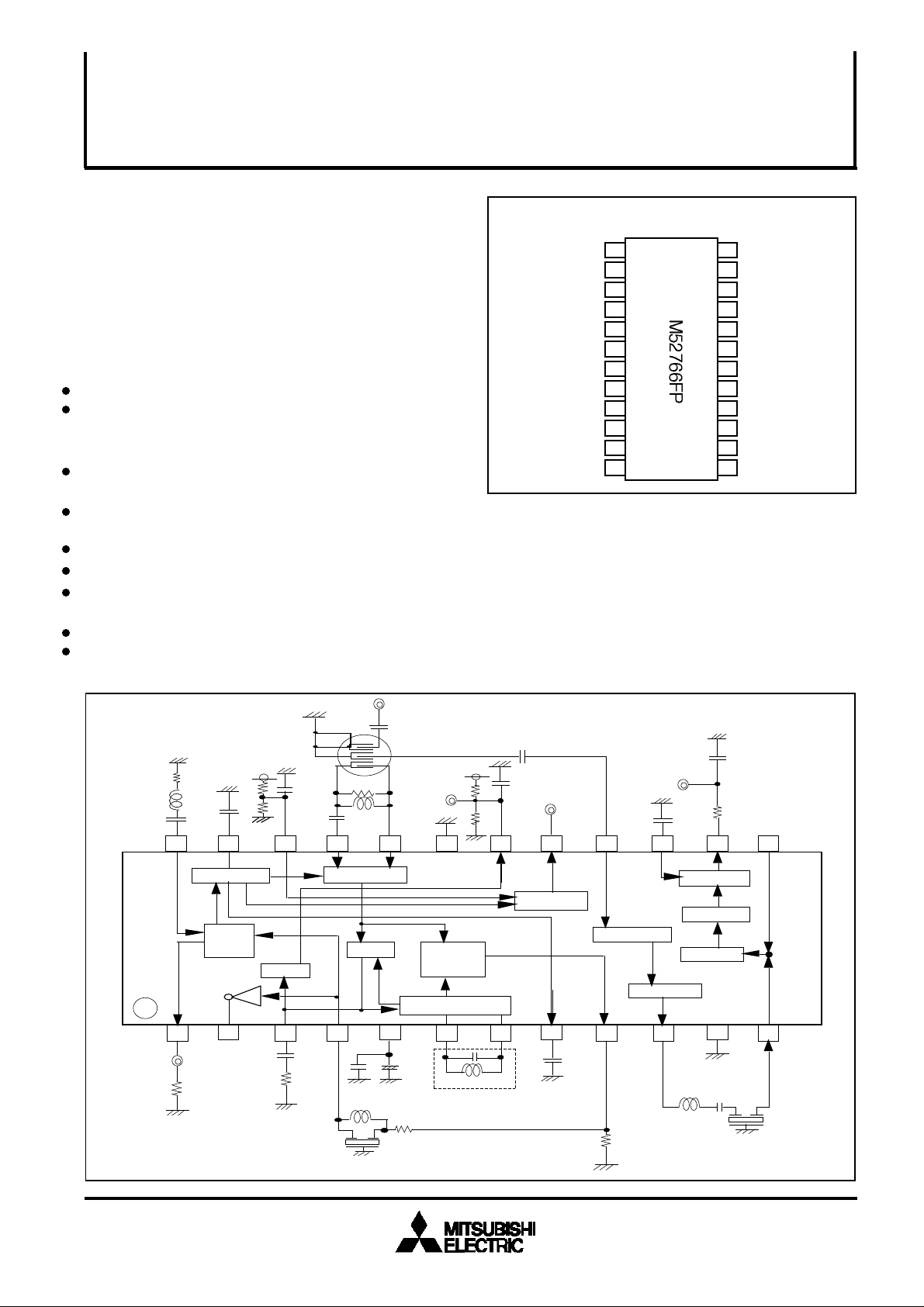
DESCRIPTION
signal,with
PLL system and no abjustment.
The N52766FP correspond to PLL split system and
intercareer system.
AFT coil is necessary.
AFT mute is not used.
The M52766FP optimum for VTR and color TV,with video
output-pin,because this IC has a built in EQ amplifier.
VCC correspond to 5V,be main strem of tuner in future.
Flat package is 24-pin SSOP of mini flat (0.8mm pich ),
suitable for space saving.
The M52766FP is a semiconducttor IC with PLL system of
VIF/ SIF.
The circuit includes video UF amplifier,PLL video
detector,IFAGC,RFAGC,VCO,AFT,LOCK
DET,EQ,REG,QIFamplifier,QIF detector,QIF AGC,LIM,FM
detector function.
The circuit realize no abjustment SIF,nothing coil AFT.
FEATURES
Dynamic AGC realizes high speed AGC with double filtre.
The M52766FP can correspond to 2tipe sound career,from
change on standard board,with sound LIM input have
2pins (12,13pin).
Sound FM detection can correspond to wide SIF
MITSUBISHI ICs (TV)
M52766FP
PLL SPLIT VIF / SIF
PIN CONFIGURATION (TOP VIEW)
EQ OUT
VIDEOINV.OUT
APC FILTER
EQ IN
VCO COIL
VCO COIL
IF AGC FILTER
VIDEO OUT
QIF OUT
LIMITER IN (NTSC)
APPLICATION
VCC
GND
10
11
12
1
2
3
4
5
6
7
8
9
24
23
22
21
20
19
18
17
16
15
14
13
EQF/B
IF AGC FILTER
RF AGC DELAY
VIF IN
VIF IN
GND
AFT OUT
RF AGC OUT
QIF DET IN
NFB
AUDIO OUT
LIMITER IN(PAL)
BLOCK DIAGRAM
IF AGC
EQ
AMP
RF AGC
Delay
Vcc
AFT
IF IN
VIF AMP
APC
AFT
OUT
VIDEO
DET
Vcc
VCO
TV sets, VTR tuners.
RECOMMEND OPERATING CONDITION
Supply voltage range • • • • 5.0 ± 0.25V
Recommended supply voltage • • • 5.0V
RF AGC
OUT
RF AGC
AF OUT
131415161718192021222324
AF AMP
FM DET
QIF AMP
LIM AMP
QIF DET
EQ OUT
1
2
3
4 5 6 7 8 9 10 11 12
+
4.5MHz Trap
Vcc
VIDEO OUT
4.5MHz Filter
( / 15 )
1
Page 2
MITSUBISHI ICs (TV)
*
PLL SPLIT VIF / SIF
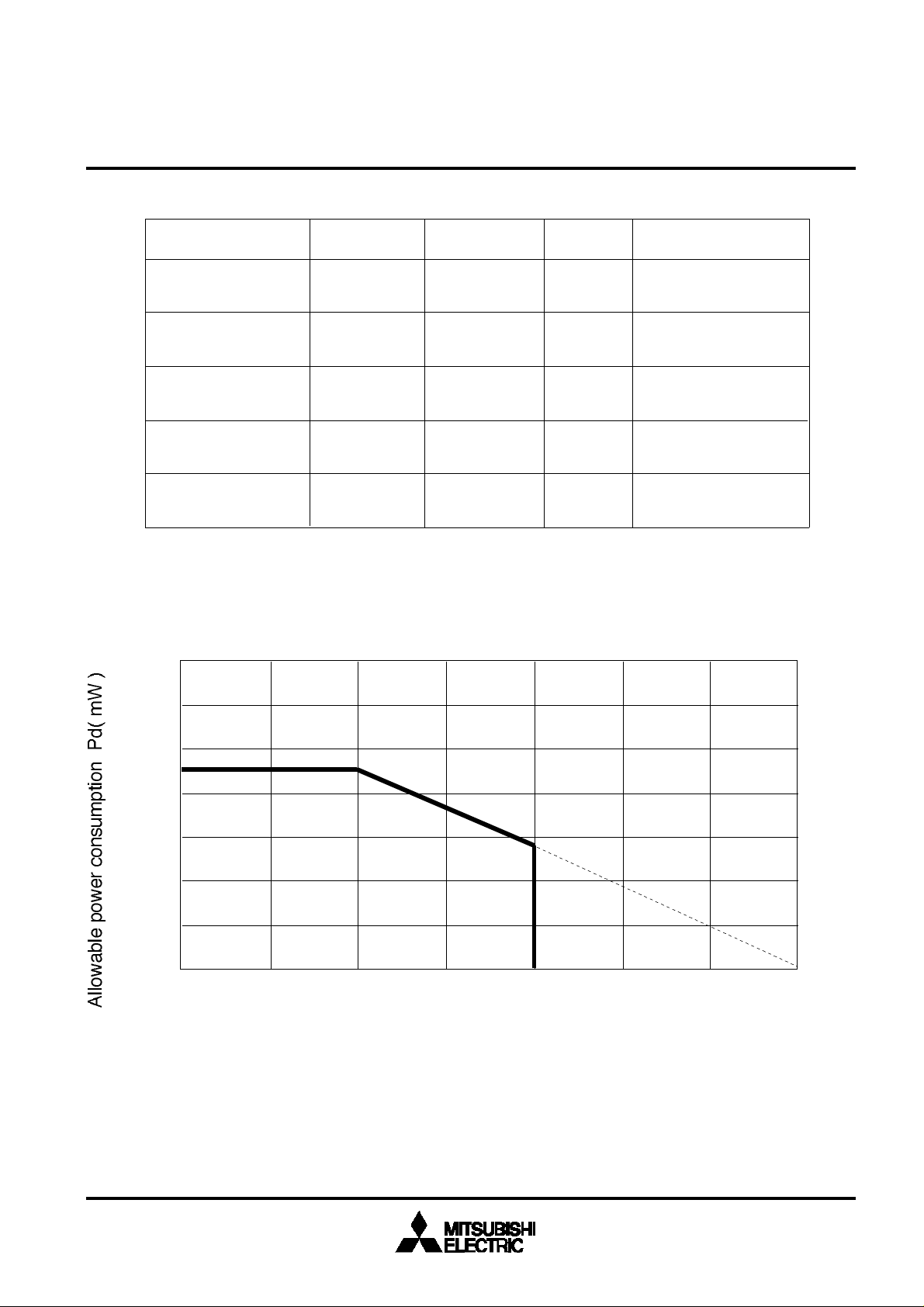
Absolute maximum ratings ( Ta = 25°C, unless otherwise noted )
M52766FP
Parameter
Symbol
Ratings Unit
Supply
Voltage 1
Power
Vcc
Pd
6.0
1524 mW
Consumption
Operating
Temperature
Storage
Temperature
Surge voltage
Topr
Tstg
Surge
-20 to +75
-40 to +150
±200
resistance
There is not all pins problem about surge, but the case of use
pay attention about latch up because the ninth pin is weak a few.
Temperature Characteristics ( maximum ratings )
Mounting in standard circuit board
1750
V
°C
°C
V
Note
surge protection
capacitance 200pF
resistance 0Ω
1500
1250
1190
1000
750
500
250
0
-20
0 25 50 75 100 125
Ambient temperature Ta (°C )
Recommended Operating Condition
( Ta = 25°C, unless otherwise noted )
Supply Voltage Range (Vcc) • • • • • 4.75 to 5.25 V
714
150
Rated Supply Voltage (Vcc) • • • • • • 5.0 V
( / 15 )
2
Page 3
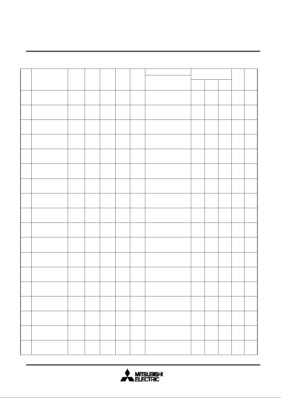
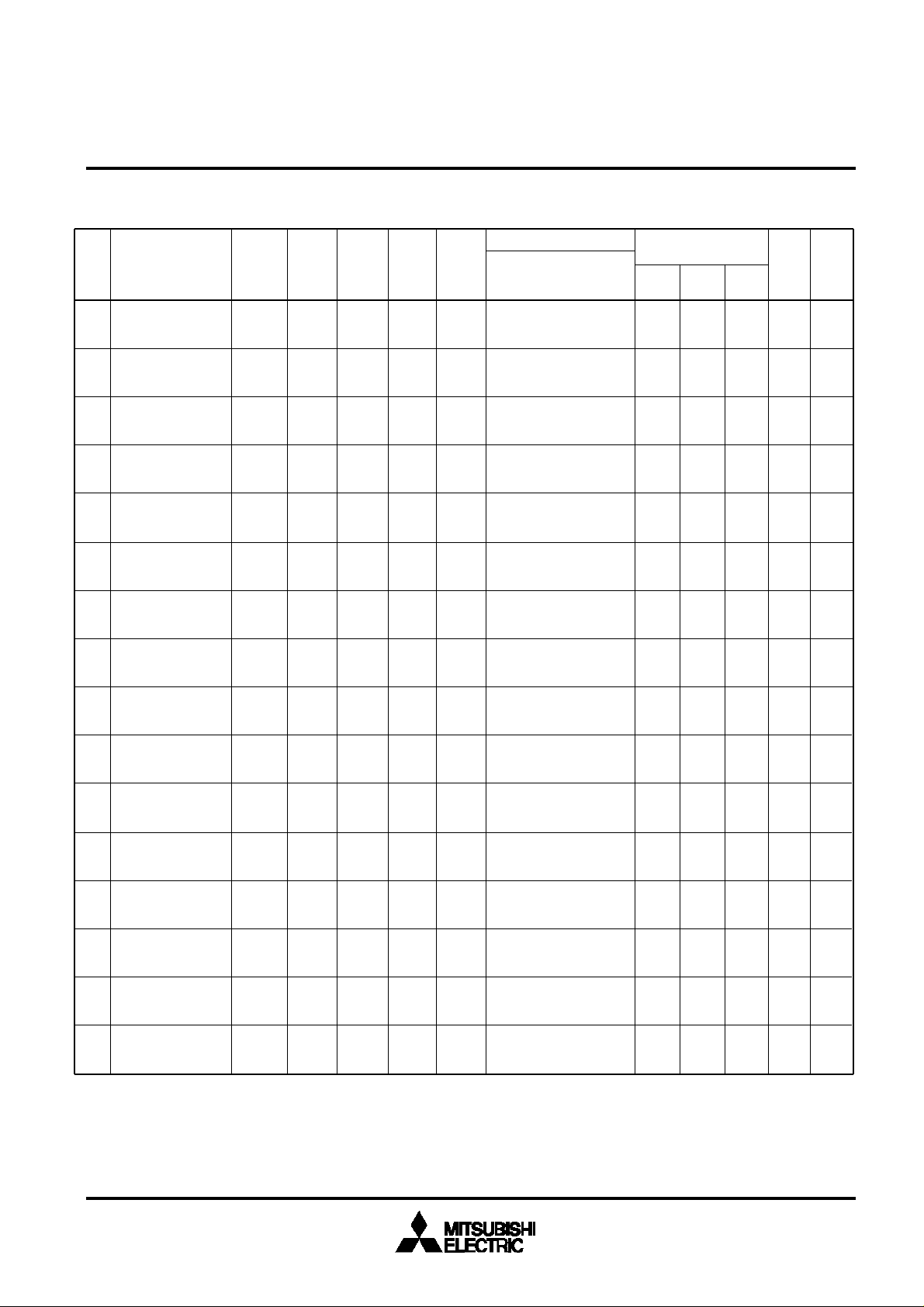
Electrical Characteristics (Vcc=5V,Ta=25°C unless otherwise noted)
VIF Section
Measurement
No. Parameter Symbol
Test
Circuit
Test
Point
Input
Point
Input
SG
switches set to position 1
unless otherwise noted
MIN TYP MAX
MITSUBISHI ICs (TV)
M52766FP
PLL SPLIT VIF / SIF
Limits
Unit Note
Circuit Current 1
1
Vcc=5V
Video Output
2
DC Voltage 1
Video Output
3
Voltage 9
Video Output
4
Voltage 1
5
Video S/N
6
Video Band Width
Input Sensitivity
7
Maximum Allowable
8
Input
AGC Control
9
Range Input
10
IF AGC Voltage 1
Icc1 1
V1 1
Vo det9
Vo det 1
Video
S/N
BW
VIN
MIN
VIN
MAX
GR – – – – dB 5
V23
1
1
1
1
1 TP1A
1
A
TP1A
TP9
TP1A
TP1B
TP1A
TP1A
TP23
– –
– –
VIF
SG1 1.1
IN
VIF
SG1
IN
VIF
SG2
IN
VIF
SG3
IN
VIF
SG4
IN
VIF
SG5
IN
VIF
SG6 V
IN
SW5=2 56
SW23=2
V23=0V
SW1=2
SW23=2
V23=Variable
40 72
3.1
0.85
1.77
51
5.0
–
101
50
2.47 3.03
2.75
3.5
2.1
56
7.0
48
105
57
3.9
1.35
2.43
–
–
52
–
–
mA
V
Vp-p
Vp-p
dB 1
MHz 2
dBµ 3
dBµ 4
Maximum IF AGC
11
Voltage 1
Minimum IF AGC
12
Voltage 1
Maximum RF AGC
13
Voltage
Minimum RF AGC
14
Voltage
RF AGC
15
Delay Point
Capture Range
16
Capture Range
17
Capture Range
18
V23H
V23L
V17H
V17L
V17
U
L
T
CL-U 1 TP1A
CL-L 1 TP1A
CL-T 1 – – – MHz 9
1
TP23
1
TP23
1
TP17
1
TP17
1
TP17
VIF
VIF
VIF
VIF
VIF
VIF
––
SG7 V
IN
SG6
IN
SG7
IN
SG8
IN
SG9
IN
SG9
IN
4.75
4.35
2.25
2.06 2.45
4.75
4.13
–
80 86
0.9
1.3
2.5
0.1
83
1.5
1.8
3.3
V
–
V
–
V
0.5
dBµ 6
MHz 7
–
MHz 8
–
–
( / 15 )
3
Page 4
MITSUBISHI ICs (TV)
M52766FP
PLL SPLIT VIF / SIF
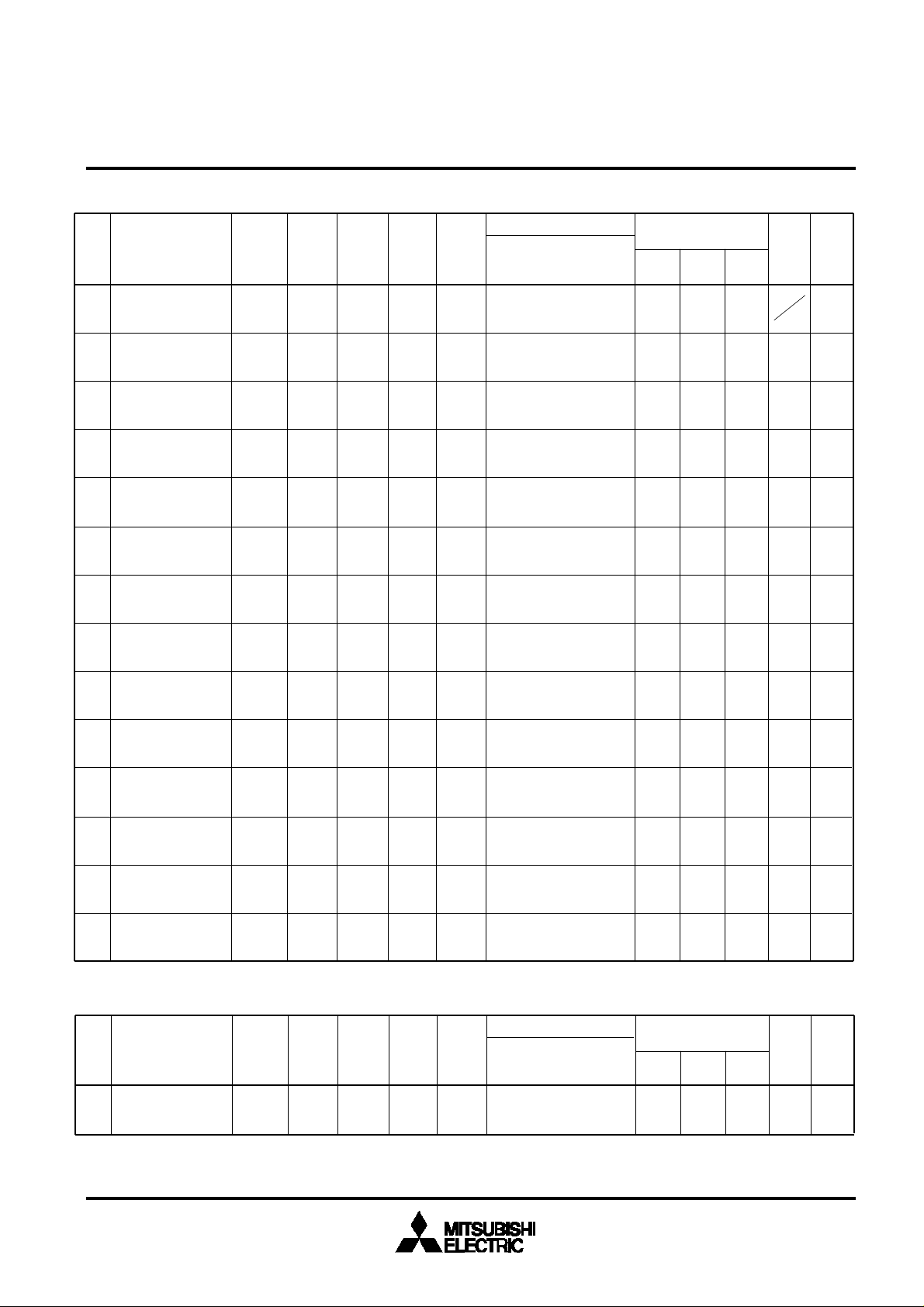
No. Parameter Symbol
19
AFT Sensitivity
AFT Maximum
20
Voltage
AFT Minimum
21
Voltage
AFT defeat
22
Inter Modulation
23
Differential
24
Gain
Differential
25
Phase
Sync. tip level
26
µ 1 TP18
V18H 1 TP18
V18L
AFT
def 1
DG 1
DP 1
V9
SYNC
Test
Circuit
1
1
1
Test
Point
TP18
TP18
TP1AIM 1
TP1A
TP1A
TP1A
Input
Point
VIF
IN
VIF
IN
VIF
IN
VIF
IN
VIF
IN
VIF
IN
VIF
IN
VIF
IN
Measurement
Input
SG
SG10
SG10
SG10 V 10
SG11
SG12
SG12
switches set to position 1
unless otherwise noted
–
SW23=2
V23=Variable
SG2
Limits
MIN TYP MAX
30
20 70
3.85
0.95 1.75
4.15
–
0.7
2.5
2.2 2.8
33
–
–
1.35
40
–
1.2
–
2
2
5
5
Unit Note
mV
kHz
V
V
dB 11
%
deg
V
10
10
VIF Input
27
Resistor
VIF Input
28
capacitance
IF AGC Voltage 2
29
Maximum IF AGC
30
Voltage 2
Minimum IF AGC
31
Voltage 2
Video Inversion
32
Output Voltage
RINV
CINV
V8
V8
V8
Vo det
INV
Control Section
No. Parameter Symbol
33 QIF Control
QIF 1
C
2
2
1
1
1
1
Test
Circuit
TP20 kΩ
TP20 pF
TP8
TP8
TP8
TP2
VIF
IN
VIF
IN
VIF
IN
VIF
IN
SG6
–
SG7
SG1
Measurement
TP16
Input
Point
Input
SG
switches set to position 1
unless otherwise noted
– –
SW16=2
Test
Point
–
1.2
–
––
5
2.75
2.40 3.11
4.25
3.80
2.25
1.95 2.55
0.25 0.75
0.5
–
Limits
MIN TYP MAX
Vp-p
Unit Note
V
V
V
V
15– 0.7 1.0
( / 15 )
4
Page 5
Electrical Characteristics (Vcc=5V,Ta=25°C unless otherwise noted)
SIF Section
Measurement
No. Parameter Symbol
Test
Circuit
Test
Point
Input
Point
Input
SG
switches set to position 1
unless otherwise noted
MIN TYP MAX
MITSUBISHI ICs (TV)
M52766FP
PLL SPLIT VIF / SIF
Limits
Unit Note
QIF Output
34
Voltage 1
QIF Output
35
Voltage 2
SIF Detection
36
Output
AF Output
37
DC Voltage
AF Output
38
(4.5MHz)
AF Output
39
(5.5MHz)
AFOutput Distortion
40
41
42
43
(4.5MHz)
AFOutput Distortion
(5.5MHz)
Limiting Sensitivity
(4.5MHz)
Limiting Sensitivity
(5.5MHz)
QIF1
QIF2
Vos 1 TP10
V1 1
VoAF
1
VoAF
2
THD
AF 1
THD
AF 2
LIM
1
LIM
2
11TP10
TP10
TP14
1
TP14
1
TP14
1
TP14
1 TP14
1 TP14
1
TP14
VIF IN
QIF IN
VIF IN
QIF IN
VIF
IN
SIF
IN
SIF
IN
SIF
IN
SIF
IN
SIF
IN
SIF
IN
SIF
IN
SG2
SG13
SG2
SG14
SG15
SG19
SG16
SG21
SG16
SG21
SG17
SG22
SW16=2
V16=0V
SW13=2
SW2=2
SW12=2
SW13=2
SW2=2
SW12=2
SW13=2
SW2=2
SW12=2
104 116
110
100
94
100
94 106
800
571 1142
730
521 1043
–
–
0.6
–
–
2.1
42
42
106
2.71.5
1.2
1.0
55
55
dBµ
dBµ
dBµ
V
mVrms
mVrms
%0.8
%
dBµ
dBµ
12
12
AM Rejection
44
(4.5MHz)
AM Rejection
45
(5.5MHz)
AF S/N (4.5MHz)
46
47
AF S/N (5.5MHz)
SIF Input
48
Resistor
SIF Input
49
Capacitance
AMR
1
AMR
2
AF
S/N 1
AF
S/N 2
RINS
CINS
1 TP14 SG18
1 TP14 SG23
1 TP14
1 TP14
2
TP16
2 TP16
SIF
IN
SIF
IN
SIF
SG19 dB 14
IN
SIF
SG24
IN
SW13=2
SW2=2
SW12=2
SW13=2
SW2=2
SW12=2
53
54
53
54
–
–
62
64
62
64
0.7
4
–
dB
–
dB
–
–
dB
–
kΩ
–
pF
( / 15 )
5
13
13
14
Page 6

Measuring Circuit Diagram 1
VIF IN
*
*
MITSUBISHI ICs (TV)
M52766FP
PLL SPLIT VIF / SIF
V23
V23
2
0.22u
TP23
1
IF AGC
EQ
AMP
Vcc
33K
27K
AFT
51
1:1
VIF AMP
APC
TP18
Vcc
150K
150K
VIDEO
DET
VCO
V16
TP17
RF AGC
2
1
0.1u
20K
QIF AMP
QIF DET
51
TP14
AF AMP
LIM AMP
FM DET
51
2
1
SW13
131415161718192021222324
SW1
1
TP1A
2
L
P
F
TP1B
1 2 3 4 5 6 7 8 9 10 11 12
+
33u
330
5549
SW5
TP8
470
1
A
2
TP10
TP9
Vcc
1
1K
1 2
TP2
SW2
0.1u
51
15u
4.5M Trap
All capacitor is 0.01µF, unless otherwise noted.
The Measuring Circuit 1 is Mitsubishi standard evaluation fixture.
( / 15 )
SW12
2
51
6
Page 7

MITSUBISHI ICs (TV)
Measuring Circuit Diagram 2
*
M52766FP
PLL SPLIT VIF / SIF
Lo
RX
meter
IF AGC
EQ
AMP
AFT
1 2 3 4 5 6 7 8 9 10 11 12
Hi
VIF AMP
APC
TP20
RF AGC
VIDEO
DET
VCO
RX
meter
Lo
Hi
TP16
131415161718192021222324
AF AMP
FM DET
QIF AMP
LIM AMP
QIF DET
All capacitor is 0.01µF, unless otherwise noted.
Vcc
+
( / 15 )
7
Page 8

INPUT SIGNAL
SG
1
f0 = 58.75 MHz AM 20 KHz 77.8 % 90 dBµ
MITSUBISHI ICs (TV)
M52766FP
PLL SPLIT VIF / SIF
50 Ω Termination
2
3
4
5
6
7
8
9
10
11
12
f0 = 58.75 MHz 90 dBµ Cw
f1 = 58.75 MHz 90 dBµ Cw
Mixed Signal
f2 = Frequency Variable 70 dB Cw
f0 = 58.75 MHz AM 20 KHz 77.8% Level Variable
f0 = 58.75 MHz AM 20 KHz 14.0% Level Variable
f0= 58.75 MHz 80 dBµ Cw
f0 = 58.75 MHz 110 dBµ Cw
f0 = 58.75 MHz Cw Level Variable
f0 = Frequency Variable AM 20 KHz 77.8 % 90 dBµ
f0 = Frequency Variable 90 dBµ Cw
f1 = 58.75 MHz 90 dBµ Cw
f2 = 55.17 MHz 80 dBµ Cw
Mixed Signal
f3 = 54.25 MHz 80 dBµ Cw
f0 = 58.75 MHz 87.5 % TV modulation Ten-step waveform
Sync Tip Level 90 dBµ
13
14
15
16
17
18
19
20
21
22
23
24
25
f1 = 54.25 MHz 95 dBµ Cw
f1 = 54.25 MHz 75 dBµ Cw
f1 = 58.75 MHz 90 dBµ Cw
Mixed Signal
f2 = 54.25 MHz 70 dBµ Cw
f0 = 4.5 MHz 90 dBµ FM 400 Hz ±25 KHzdev
f0 = 4.5 MHz Level Variable FM 400Hz ±25KHzdev
f0 = 4.5 MHz 90 dBµ AM 400 Hz 30 %
f0 = 4.5 MHz 90 dBµ Cw
f0 = 4.5 MHz Level Variable Cw
f0 = 5.5 MHz 90 dBµ FM 400 Hz ±50 KHzdev
f0 = 5.5 MHz Level Variable FM 400Hz ±50KHzdev
f0 = 5.5 MHz 90 dBµ AM 400 Hz 30 %
f0 = 5.5 MHz 90 dBµ Cw
f0 = 5.5 MHz Level Variable Cw
( / 15 )
8
Page 9

MITSUBISHI ICs (TV)
Notes
PLL SPLIT VIF / SIF
1. Video S/N
Input SG2 into VIF IN and measure the video out(Pin 1) noise in r.m.s at TP1B
through a 5MHz (-3dB) L.P.F.
M52766FP
S/N=20 log
2. Video Band Width: BW
1. Measure the 1MHz component level of Video output TP1A with a spectrum
analyzer when SG3(f2=57.75MHz) is input into VIF IN. At that time, measure
the voltage at TP23 with SW23, set to position 2, and then fix V23 at that
voltage.
2. Reduce f2 and measure the value of (f2-f0) when the (f2-f0) component level
reaches -3dB from the 1MHz component level as shown below.
TP1A
-3dB
0.7 x Vo det
NOISE
[dB]
( f2 - f0 )
1 MHz BW
3. Input Sensitivity: VIN MIN
Input SG4 (Vi=90dBµ) into VIF IN , and then gradually reduce Vi and
measure the input level when the 20KHz component of Video output TP1A
reaches -3dB from Vo det level.
4. Maximum Allowable Input: VIN MAX
1. Input SG5 (Vi=90dBµ) into VIF IN , and measure the level of the 20KHz
component of Video output.
2. Gradually increase the Vi of SG and measure the input level when the
output reaches -3dB.
( / 15 )
9
Page 10

5. AGC Control Range: GR
GR = VIN MAX - VIN MIN [dB]
6. RF AGC Operating Voltage: V17
Input SG8 into VIF IN and gradually reduce Vi and then measure the input
level when RF AGC output TP17 reaches 1/2 VCC, as shown below.
TP17
Voltage
V17H
MITSUBISHI ICs (TV)
M52766FP
PLL SPLIT VIF / SIF
1/2VCC
V17L
Vi
Vi(dBµ)
7. Capture range: CL - U
1. Increase the frequency of SG9 until the VCO is out of locked-oscillation.
2. Decrease the frequency of SG9 and measure the frequency fU when the
VCO locks.
CL - U = fU - 58.75 [MHz]
8. Capture range: CL - L
1. Decrease the frequency of SG9 until the VCO is out of locked-oscillation.
2. Increase the frequency of SG9 and measure the frequency fL when the
VCO locks.
CL - L = 58.75 - fL [MHz]
9. Capture range: CL - T
CL - T = CL - U + CL - L [MHz]
( / 15 )
10
Page 11

MITSUBISHI ICs (TV)
M52766FP
PLL SPLIT VIF / SIF
10. AFT sensitivity µ, Maximum AFT voltage V18H , Minimum AFT voltage V18L
1. Input SG10 into VIF IN , and set the frequency of SG10 so that the voltage
of AFT output TP18 is 3[V] . This frequency is named f(3).
2. Set the frequency of SG10 so that the AFT output voltage is 2[V].
This frequency is named f(2)
3. IN the graph, maximum and minimum DC voltage are V18H and V18L,
respectively.
TP2
Voltage
3V
µ =
1000 [mV]
f(2) - f(3) [kHz]
[mV/kHz]
2V
V18H
f(3) f(2)
11. Inter modulation: IM
1. Input SG11 into VIF IN, and measure video output TP9 with an oscilloscope.
2. Adjust AGC filter voltage V23 so that the minimum DC level of the output
waveform is 1.0V.
3. At this time, measure TP9 with a spectrum analyzer .
The inter modulation is defined as a difference between 0.92MHz and
3.58 MHz frequency components.
V18L
f(MHz)
( / 15 )
11
Page 12

MITSUBISHI ICs (TV)
PLL SPLIT VIF / SIF
12. Limiting Sensitivity: LIM
1. Input SG17 (SG22) into SIF input, and measure the 400Hz component level
of AF output TP14.
2. Input SG20 (SG25) into SIF input, and measure the 400Hz component level
of AF output TP14 .
3. The input limiting sensitivity is defined as the input level when a difference
between each 400Hz components of audio output (TP14) is 30dB, as shown
below.
Audio Output
M52766FP
(mVrms)
30dB
Audio output while SG17 (SG22) is input.
Audio output while SG20 (SG25) is input.
(dBµ)
SIF Input
13. AM Rejection: AMR
1. Input SG18 (SG23) into SIF IN ,and measure the output level of Audio output
(TP12). This level is named VAM.
2. AMR is;
AMR = 20log
VoAF (mVr.m.s)
VAM (mVr.m.s)
[dB]
14. AF S/N: AF S/N
1. Input SG19 (SG24) into SIF input ,and measure the output noise level of Audio
output (TP14). This level is named VN.
2. S/N is;
VoAF (mVr.m.s)
S/N = 20log
VN (mVr.m.s)
[dB]
15. QIF Control : CQIF
Lower the voltage of V16 ,and measure the voltage of V16 when DC voltage of
TP10 begins to change.
( / 15 )
12
Page 13

0
1 2
3 4
8
Structure of package (Cross section)
MITSUBISHI ICs (TV)
M52766FP
PLL SPLIT VIF / SIF
Structure
Matrrial
Inner Lead Plating
Die Bond
Lead Flame
Lead Flame
Mold resin : Epoxy resin
Internal lead : Au wire ( 25µm)
External lead plating : Solder plating
Lead frame : Copper alloy
Passivation : Nitride coat
Outer Passivation
Pellet
Plastic Molding
Wire
Back Metalize
Lead Flame
Manufacturing place (Wafer process,assembly,final inspection)
Mitsubishi Electric Corporation Fukuoka Semiconductor Factory
Indications
M 5 2 7 6 6 F P
Lot number constitution
The first place of the year
(1998)
X X X X X X
weekly code
(12th week)
Model Number
Mark lot number
Production
factory code
Running number
( / 15 )
13
Page 14

Package specification
IC package : 24P2Q
MITSUBISHI ICs (TV)
M52766FP
PLL SPLIT VIF / SIF
In case of tube shipping
Tube : 50 pieces / tube
Interior box : 5000 pieces / interior box
(100 tubes / interior box)
Exterior box : 20000 pieces / exterior box
(4 interior boxes / exterior box)
The packing method in case of tube shipping
1. Container tube
1.1 Container tube size
(1) IC tube MP016PC
A cross section
13
In case of emboss tape shipping
(The direction of T1)
Reel : 2000 pieces / reel
Interior box : 1 reel / interior
Exterior box : 10000 pieces / exterior box
(5 interior boxes / exterior box)
(2) Stopper plug
6.4
Width : 5.5
Color : Gray
Total length
Stopper plug
550
Unit : (mm)
14
( / 15 )
Page 15

1.2 Packing method
***
*
(1) The packing direction of the device.
(Facing the Pin No.1 with the marking side as shown below.)
MITSUBISHI ICs (TV)
M52766FP
PLL SPLIT VIF / SIF
Pin No.1
(2) The prevention of the vibration damage.
The stopper plug is pushed into the tube so that devices should
not move and are kept plain condition.
Take care they do not warp.
(3) In case of a fraction
In case IC number does not fill the typical accommodations, the stopper
plug is used to fix devices.
"PARTIAL"label is stuck on the fraction tube as shown below.
PARTIAL
2. Interior box and exterior box
2.1 The arrangement of tubes in the interior box.
The marking side of the tube
A position of the stopper plug.
Nine lines and twelve steps
117
2.2 Damp proof packing
Use the specified PE bag and put a silica gel in it.
Put the sealed interior box in a PE bag.
Put the silica gel on the top step in the box.
One line is in top step.
Unit (mm)
( / 15 )
15
 Loading...