

Page 1
MITSUBISHI ICs (TV)
M52760SP
PLL-SPLIT VIF/SIF IC
DESCRIPTION
The M52760SP is IF signal-processing IC for VCRs and TVs. It
enable the PLL detection system despite size as small as that of
conventional quasi-synchronous VIF/SIF detector, IF/RF AGC, SIF
limiter, FM detector and EQ AMP.
FEATURES
Video detection output is 2V
•
The package is a 20-pin shrink-DIP, suitable for space saving.
•
The video detector uses PLL for full synchronous detection
•
circuit. It produces excellent characteristics of DG, DP, 920kHz
beat, and cross color.
•
Dynamic AGC realizes high speed response with only single
filter.
•
Video IF and sound IF signal processings are separated from
each other. VCO output is used to obtain intercarrier.
This PLL-SPLIT method provide good sound sensitivity and
reduces buzz.
•
As AFT output voltage uses the APC output voltage, VCO coil is
not used.
Audio FM demodulation uses PLL system, so it has wide
•
frequency range with no external parts and no adjustment.
QIF AMP has a fixed gain, and good characteristic for NICAM.
•
. It has built-in EQ AMP.
P-P
APPLICATION
TV sets, VCR tuners
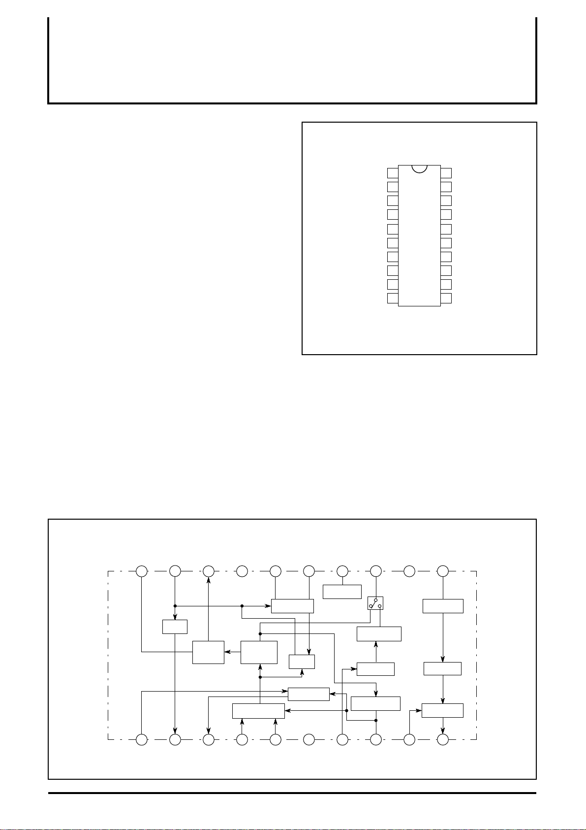
PIN CONFIGURATION (TOP VIEW)
RF AGC DELAY EQ F/B
AFT OUT
RF AGC OUT
QIF DET IN
IF AGC FILTER
AUDIO OUT
VIF IN
VIF IN
GND
NFB
1
2
3
4
Outline 20P4B
20
19
18
M52760SP
17
165
156
147
138
129
1110
APC FILTER
VIDEO OUT
Vreg. OUT
VCO COIL
VCO COIL
Vcc
QIF OUT
AFT SW/NPSW
LIMITER IN
RECOMMENDED OPERATING CONDITION
In case of Vcc and Vreg. out short
Supply voltage range....................................................4.75 to 5.25V
Recommended supply voltage...................................................5.0V
In case of Vreg. out open
Supply voltage range......................................................8.5 to 12.5V
BLOCK DIAGRAM
18
EQ
AMP
Vreg. OUT LIMITER INAPC FILTER
17 16
VCO COIL Vcc
VIDEO
DET
VIF AMP
EQ F/B AFT SW/NPSW
20
VIDEO OUT
19
AFT
VCO COIL
VCO
APC
RF AGC
QIF OUT
15
14 12
Vcc REG
13
SplitInter
QIF DET
QIF AMP
IF AGC
11
LIM AMP
FM DET
AF AMP
1
RF AGC DELAY
1
2
AFT OUT AUDIO OUTIF AGC FILTER
3
RF AGC OUT
45
6 8
QIF DET IN
GNDVIF IN
97
NFBVIF IN
10
Page 2
°
°
±
−
−
−
− dB µ
−
−
−
−
−
−
−
−
−
−
−
µ
MITSUBISHI ICs (TV)
M52760SP
PLL-SPLIT VIF/SIF IC
ABSOLUTE MAXIMUM RATINGS
(Ta=25 ° C, surge protection capacitance 200pF resistance 0 Ω , unless otherwise noted)
Symbol Parameter Ratings Unit
V
CC
Vreg
OUT
d
P
T
opr
T
stg
Surge Surge voltage resistance
AMBIENT OPERATING CONDITION
IN CASE OF V
Vreg. OUT SHORT
IN CASE OF Vreg.
OUT OPEN
ELECTRICAL CHARACTERISTICS
Supply voltage1 13.2 V
.
Supply voltage Vreg. OUT 6 V
Power dissipation 1524 mW
Operating temperature -20 to +75
Storage temperature -40 to +150
200 V
(Ta=25 ° C, unless otherwise noted)
Supply voltage Supply voltage range
AND
CC
4.75 to 5.25V 5.0V
Recommended supply
voltage
8.5 to 12.5V
(V
=5V , Ta=25 ° C, unless otherwise noted)
CC
C
C
Measurement condition
Symbol Parameter
Test
circuit
Test
point
Input
point
Input
SG
External
power supply
V12
switches set to
position 1 unless
otherwise indicatedV7 V8
Limits
Min. Typ. Max.
VIF section
CC1
I
CC2
I
CC2
V
V18 Video output DC voltage 1 TP18A −−−
o det
V
Video S/N
BW Video band width 1 TP18A VIF IN SG3 −
Circuit current1
CC
V
=5V
Circuit current2
V
=12V
CC
1 A VIF IN SG1 −− 5
1 A VIF IN SG1 −− 5
Vreg voltage 1 TP17 −−−−
0
Video output voltage 1 TP18A VIF IN SG1 −−−
Video S/N 1 TP18A VIF IN SG2 −−− SW18=2 51 56
Vari
able
CC
=5V
V
SW17=1, SW14=2
CC
V
=12.5V
SW14=SW17=2
CC
V
=12.5V
5
SW7=2
−
SW8=2 3.2 3.5 3.8 V
33 46 59 mA
33 46 59 mA
4.60 4.95 5.30 V
1.8 2.1 2.4 V
SW8=2
7.0 9.0
VIN MIN Input sensitivity 1 TP18A VIF IN SG4 −−− − 48 52 dB µ
VIN MAX
GR AGC control range input
V8 IF AGC voltage 1 TP8 VIF IN SG6 −−−
V8H
V8L
V3H
V3L
V3
CL-U Capture range U 1 TP18A VIF IN SG9 −−−
CL-L Capture range L 1 TP18A VIF IN SG9 −−−
CL-T Capture range T 1
VCO ∆ f VCO SW ON Drift 1 TP18A −−−
Maximum allowable
input
Maximum IF AGC
voltage
Minimum IF AGC
voltage
Maximum RF AGC
voltage
Minimum RF AGC
voltage
RF AGC Operation
voltage
1 TP18A VIF IN SG5 −−−
−−−−
1 TP8
−−
−−−
−−−
1 TP8 VIF IN SG7 −−−
1 TP3 VIF IN SG6 −−−
1 TP3 VIF IN SG7 −−−
1 TP3 VIF IN SG8 −−−
−
− − −−−
0
− ± 0 +20 +40 kHz
101 105
50 57
2.9 3.2 3.5 V
4.0 4.4
2.2 2.4 2.6 V
4.2 4.7
CC
=9V) 8.0 8.9
CC
(V
=12V) 11.0 11.9
− 0.1 0.5
CC
=9V)
CC
(V
=12V)
89 92 95 dB µ
1.0 1.7
1.8 2.4
3.1 4.1
0.2 0.7
0.2 0.7
AFT sensitivity 1 TP2 VIF IN SG10 −− 3.3 20 30 60 mV/kHz
Unit
P-P
dB
MHz
dB
V
V(V
V(V
MHz
MHz
MHz
2
Page 3
−
−
−
−
−
−
MITSUBISHI ICs (TV)
M52760SP
PLL-SPLIT VIF/SIF IC
−
−
−
− k Ω
−
−
ELECTRICAL CHARACTERISTICS
(cont.)
Measurement condition
Symbol Parameter
Test
circuit
Test
point
Input
point
Input
SG
External
power supply
V12
switches set to
position 1 unless
otherwise indicatedV7 V8
Limits
Min. Typ. Max.
Unit
3.85 4.15
V2H AFT maximum voltage 1 TP2 VIF IN SG10 −− 3.3
=9V) 7.7 8.1
CC
(V
=12V) 10.7 11.1
CC
V(V
0.7 1.2
V2L AFT minimum voltage 1 TP2 VIF IN SG10 −− 3.3
=9V)
CC
CC
(V
=12V)
0.7 1.2
0.7 1.2
V(V
2.2 2.5 2.8
1.65
AFT def1 AFT Defeat 1 1 TP2 VIF IN SG10 −−
CC
=9V) 4.1 4.5 4.9
CC
(V
=12V) 5.5 6.0 6.5
V(V
2.2 2.5 2.8
AFT def2 AFT Defeat 2 1 TP2 VIF IN SG10 −− 4.6
Vari
IM Inter modulation 1 TP18A VIF IN SG11
−
able
CC
=9V) 4.1 4.5 4.9
CC
(V
=12V) 5.5 6.0 6.5
SW8=2
35 40
V(V
dB
DG Differential gain 1 TP18A VIF IN SG12 −−− − 2 5 %
DP Differential phase 1 TP18A VIF IN SG12 −−− − 2 5 deg
V13
SYNC
RINV VIF input resister 2 TP4
CINV VIF input capacitance 2 TP4
Sync. tip level 1 TP18A VIF IN SG2 −−−
0.85 1.15 1.45 V
1.2
5
pF
SIF section
QIF1 QIF output 1 1 TP13
QIF2 QIF output 2 1 TP13
VIF IN
QIF IN
VIF IN
QIF IN
SG2
SG13
SG2
SG14
−−−
−−−
108 114 120 dB µ
94 100 106 dB µ
Vos SIF detection output 1 TP13 VIF IN SG15 0 − 5 SW7=2 94 100 106 dBµ
V1 AF output DC voltage 1 TP10 SIF IN SG19 −−5 1.6 2.2 2.8 V
VoAF1 AF output (4.5MHz) 1 TP10 SIF IN SG16 −−5 320 560 800 mVrms
VoAF2 AF output (5.5MHz) 1 TP10 SIF IN SG20 −−0 255 450 645 mVrms
THD AF1
THD AF2
LIM1
LIM2
AF output distortion
(4.5MHz)
AF output distortion
(5.5MHz)
Limiting sensitivity
(4.5MHz)
Limiting sensitivity
(5.5MHz)
1 TP10 SIF IN SG16 −−5 − 0.2 0.9 %
1 TP10 SIF IN SG20 −−0 − 0.2 0.9 %
1 TP10 SIF IN SG17 −−5 − 42 55 dBµ
1 TP10 SIF IN SG21 −−0 − 42 55 dBµ
AMR1 AM rejection (4.5MHz) 1 TP10 SIF IN SG18 −−5 55 62 − dB
AMR2 AM rejection (5.5MHz) 1 TP10 SIF IN SG22 −−0 55 64 − dB
AF S/N 1 AF S/N (4.5MHz) 1 TP10 SIF IN SG19 −−5 55 62 − dB
AF S/N 2 AF S/N (5.5MHz) 1 TP10 SIF IN SG23 −−0 55 64 − dB
RINS SIF input resistance 2 TP7 − 1.5 − kΩ
CINS SIF input capacitance 2 TP7 − 4 − pF
Control section
QIF QIF control 1 TP7 −−
C
Vari
able
−−
SW7=2
− 0.7 1.0 V
PIN12 VOL TAGE CONTROL
Pin12 voltage (V) AF AFT
0 to 2.3
2.7 to 5.0
3
0 to 0.6
1.0 to 2.3 DEFEAT
2.7 to 4.0
4.4 to 5.0 DEFEAT
PAL
NTSC
NORMAL
NORMAL
Page 4

MITSUBISHI ICs (TV)
M52760SP
PLL-SPLIT VIF/SIF IC
ELECTRICAL CHARACTERISTICS TEST METHOD
Video S/N
Input SG2 into VIF IN and measure the video out (Pin 18) noise in
r.m.s at TP18B through a 5MHz (-3dB) L.P.F.
S/N=20 log
0.7×Vo det
NOISE
BW Video band width
1. Measure the 1MHz component level of EQ output TP18A with a
spectrum analyzer when SG3 (f2=57.75MHz) is input into VIF
IN. At that time, measure the voltage at TP8 with SW8, set to
position 2, and then fix V8 at that voltage.
2. Reduce F2 and measure the value of (f2-f0) when the (f2-f0)
component level reaches -3dB from the 1MHz component level
as shown below.
TP18
-3dB
(dB)
V3 RF AGC operating voltage
Input SG8 into VIF IN, and gradually reduce Vi and then measure
the input level when RF AGC output TP3 reaches 1/2 V
CC, as
shown below.
TP3
Voltage
3H
V
1/2VCC
V
3L
Vi
Vi (dBµ)
CL-U Capture range
1. Increase the frequency of SG9 until the VCO is out of lockedoscillation.
2. Decrease the frequency of SG9 and measure the frequency fU
when the VCO locks.
CL-U=fU-58.75 (MHz)
1MHz
BW
( f2 - f0 )
VIN MIN Input sensitivity
Input SG4 (Vi=90dBµ) into VIF IN, and then gradually reduce Vi and
measure the input level when the 20kHz component of EQ output
TP18A reaches -3dB from Vo det level.
VIN MAX Maximum allowable input
1. Input SG5 (Vi=90dBµ) into VIF IN, and measure the level of the
20kHz component of EQ output.
2. Gradually increase the Vi of SG and measure the input level
when the output reaches -3dB.
GR AGC control range
GR=VIN MAX-VIN MIN (dB)
CL-L Capture range
1. Decrease the frequency of SG9 until the VCO is out of lockedoscillation.
2. Increase the frequency of SG9 and measure the frequency fL
when the VCO locks.
CL-L=58.75-fL (MHz)
CL-T Capture range
CL-T=CL-U+CL-L (MHz)
VCO ∆f VCO SW on drift
1. Input SG2 into VIF IN .
2. Adjust the VCO coil so that AFT voltage can be reached to 1/2
Vcc in 10 seconds after the power switch is turned to on.
3. IF AGC FILTER (Pin8) is connected to GND (0V) after turning off
the VIF input.
4. And then, measure each free running frequencies of 10 and 60
seconds later.
VCO ∆f (kHz) = frequency2 (60 sec. later)
-frequency1 (10 sec. later)
4
Page 5

MITSUBISHI ICs (TV)
AMR=20log
VoAF (mVr.m.s)
VAM (mVr.m.s)
(dB)
M52760SP
PLL-SPLIT VIF/SIF IC
µ AFT sensitivity , V2H Maxim um AFT v olta ge, V2L Minimum AFT
voltage
1. Input SG10 into VIF IN , and set the frequency of SG10 so that
the voltage of AFT output TP2 is 3V. This frequency is f (3).
2. Set the frequency of SG10 so that the AFT output voltage is 2V.
This frequency is f (2)
3. IN the graph, maximum and minimum DC voltage are V
2H and
V2L, respectively.
TP2
Voltage
3V
V2H
2V
V2L
f (3) f (2) f (MHz)
1000 (mV)
µ =
f (2) - f (3) (kHz)
(mV/kHz)
IM Intermodulation
1. Input SG11 into VIF IN, and measure EQ output TP18A with an
oscilloscope.
2. Adjust AGC filter voltage V8 so that the minimum DC level of the
output waveform is 1.0V.
3. At this time, measure, TP18A with a spectrum analyzer.
The intermodulation is defined as a difference between 1.07MHz
and 4.43MHz frequency components.
LIM Limiting sensitivity
1. Input SG17 (SG21) into SIF input, and measure the 400Hz
component level of AF output TP10.
2. Input SG19 (SG23) into SIF input, and measure the 400Hz
component level of AF output TP10.
3. The input limiting sensitivity is defined as the input level when a
difference between each 400Hz components of audio output
(TP10) is 30dB, as shown below.
AMR AM Rejection
1. Input SG18 into SIF input, and measure the output level of AF
output TP10. This level is V AM.
2. AMR is;
AF S/N
1. Input SG19 into SIF input, and measure the output noise level of
AF output TP1. This level is VN.
2. S/N is;
C
QIF QIF control
S/N=20log
VoAF (mVr.m.s)
VN (mVr.m.s)
(dB)
Lower the voltage of V7, and measure the voltage of V7 when the
DC voltage of TP13 begins to change.
THE NOTE IN THE SYSTEM SETUP
M52760SP has 2 power supply pins of Vcc (pin 14) and Vreg.OUT
(pin 17) .
Pin 14 is for AFT output, RF AGC output circuits and 5V regulated
power supply circuit and Pin 17 is for the other circuit blocks.
In case M52760SP is used together with other ICs like VIF
operating at more than 5V, the same supply voltage as that of
connected ICs is applied to VCC and Vreg.Out is opened. The other
circuit blocks, connected to Vreg.OUT are powered by internal 5V
regulated power supply.
In case the connecting ICs are operated at 5V, 5V is supplied to
CC and Vreg.OUT.
both V
LOGIC T ABLE
AF AFT
10k “H”
10k “L”
20k “H”
20k “L” NORMAL
20k “H”
20k “L” NORMAL
NTSC
PAL
DEFEAT
DEFEAT
Audio output
(mVrms)
5
30dB
Audio output while
SG17 (SG21) is input
Audio output while
SG19 (SG23) is input
SIF input
(dBµ)
Page 6

MITSUBISHI ICs (TV)
AMBIENT TEMPERATURE Ta (°C)
0 25 50 75 100 125
0
250
500
750
1000
1750
150-20
1250
1500
914
THERMAL DERATING (MAXIMUM RATING)
POWER DISSIPATION Pd (mW)
1524
PLL-SPLIT VIF/SIF IC
INPUT SIGNAL TYPICAL CHARACTERISTICS
SG No. Signals (50Ω termination)
1f0=58.75MHz AM20kHz 77.8% 90dBµ
2f0=58.75MHz 90dBµ CW
1=58.75MHz 90dBµ CW (Mixed signal)
f
3
f2=Frequency variable 70dBµ CW (Mixed signal)
4f0=58.75MHz AM20kHz 77.8% level variable
5f0=58.75MHz AM20kHz 14.0% level variable
6f
7f0=58.75MHz 110dBµ CW
8f0=58.75MHz CW level variable
9f0=Variable AM20kHz 77.8% 90dBµ
10 f0=Variable 90dBµ CW
11
12
13 f1=54.25MHz 95dBµ CW
14 f1=54.25MHz 75dBµ CW
15
16 f0=4.5MHz 90dBµ FM400Hz±25kHz dev
17 f0=4.5MHz FM400Hz±25kHz dev level variable
18 f0=4.5MHz 90dBµ AM400Hz 30%
19 f0=4.5MHz 90dBµ CW
20 f0=5.5MHz 90dBµ FM400Hz±50kHz dev
21 f0=5.5MHz FM400Hz±50kHz dev level variable
22 f0=5.5MHz 90dBµ AM400Hz 30%
23 f0=5.5MHz 90dBµ CW
0=58.75MHz 80dBµ CW
f1=58.75MHz 90dBµ CW (Mixed signal)
f2=55.17MHz 80dBµ CW (Mixed signal)
f3=54.25MHz 80dBµ CW (Mixed signal)
f0=58.75MHz 87.5%
TV modulation ten-step waveform
sync tip level 90dBµ
1=58.75MHz 90dBµ CW (Mixed signal)
f
f2=54.25MHz 70dBµ CW (Mixed signal)
M52760SP
6
Page 7

APPLICATION EXAMPLE 1
0.47µ
TP18A
SW18
62
TP18B
L
P
F
12
82p
390k
SW17
made by Toko
33µ
1
2
5549
SW14
1
2
TP13
MITSUBISHI ICs (TV)
M52760SP
PLL-SPLIT VIF/SIF IC
A
SIF IN
V12
TP12
0.01µ
V
CC
51
30k
20k
TP2
20
1
TP1
150k
150k
19
AFT
2
39k
18
EQ
AMP
3
V
CC
17 16 14
VIDEO
DET
VIF AMP
45 97
TP3
1:1
51
VIF IN
15
VCO
APC
RF AGC
68
0.01µ
51
Vcc REG
SW7
12
TP7
QIF DET
QIF AMP
IF AGC
0.47µ
V7
V8
SplitInter
TP8
12
SW8
12
10µ
1113
LIM AMP
FM DET
AF AMP
10
7.5k2.4k
TP10
0.01µ
∗ Capacitors without an assignment are 0.01µF.
∗ The Measuring Circuit 1 is Mitsubishi standard evaluation fixture.
Units Resistance : Ω
Capacitance : F
7
Page 8

APPLICATION EXAMPLE 2
MITSUBISHI ICs (TV)
M52760SP
PLL-SPLIT VIF/SIF IC
20
1
∗ All capacitor is 0.01µF, unless otherwise specified.
19
AFT
2
18
EQ
AMP
3
17 16 14
VIDEO
DET
VIF AMP
45 97
TP4
HI
RX
meter
LO
15
Vcc REG
VCO
APC
RF AGC
68
HI
LO
QIF DET
QIF AMP
IF AGC
TP7
RX
meter
SplitInter
12
1113
LIM AMP
FM DET
AF AMP
10
8
 Loading...