

Page 1
MITSUBISHI <LINEAR IC>
PROVISINAL INFORMATION M52759SP
UNIFORMITY FOR CRT DISPLAY MONITOR
DESCRIPTION
M52759SP is Semiconductor Integrated Circuit
for uniformity of CRT Display Monitor.
It generates horizontal and vertical parabola waves and
is able to revise contrast of CRT Display Monitor if it is
used with Video Pre. Amp. M52742SP that has uniformity
circuit .
FEATURES
• It can control phase of horizontal wave.
• It can changes the parabola wave unbalance .
• It contains the horizontal saw wave generator and Auto
Gain Control circuit , so that it is able to keep the amplitude
constant if frequency change.
• It can changes the parabola wave unbalance .
• Frequency Band Width: horizontal 24 to 120kHz
vertical 50 to 185Hz
• Input: horizontal 5Vp-p Pulse
vertical 3.2 Vp-p V Saw
STRUCTURE
Bipolar Silicon Monolisic IC
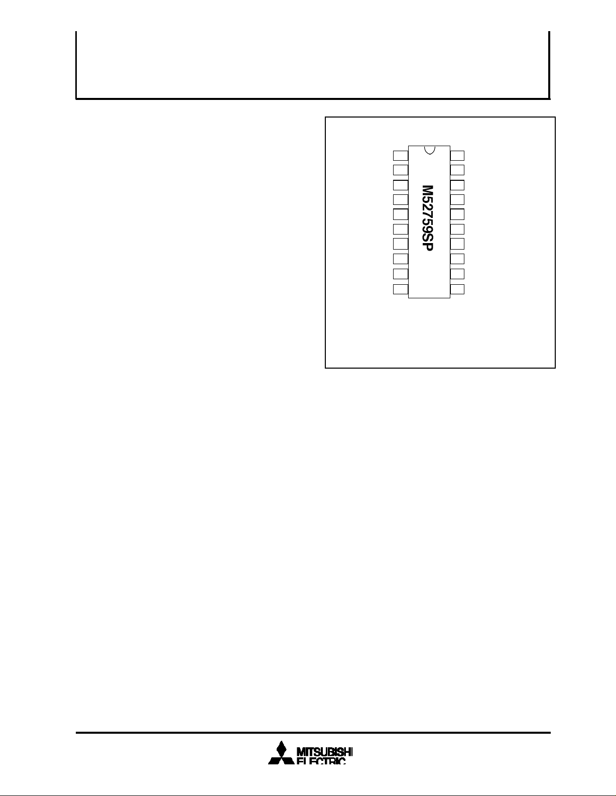
PIN CONFIGURATION (TOP VIEW)
V-GND
V-saw input
Vbias
V-para output
VGV input
VGH input
H-para output
H- Saw retrace
H- Saw trace
H-Vcc
1
2
3
4
5
6
7
8
9
Package:20P4B
V-Vcc
20
19
Hbias
H-GND
18
H-Pulse input
17
H-Delay Capacitor
16
VPH input
15
Reference Voltage
14
Reference Voltage Resistor
13
AGC trace Capacitor
12
AGC retrace Capacitor
1110
APPLICATION
CRT Display Monitor
Supply voltage range
11.5V to 12.5V
Rated supply voltage
12V
( / 25 )
1
Page 2
MITSUBISHI <LINEAR IC>
PROVISINAL INFORMATION M52759SP
UNIFORMITY FOR CRT DISPLAY MONITOR
Application Example
1.8k
100p
Flyback
Pulse in
+
3.9k
1k
1k
Vcc 12V
V-Vcc
V-GND
20
1
Hbias
Para.Amp
2
X
2 3 4 5
Vbias
V-Saw
input
Buffer
Vout
H-Pulse
VGV
(V Gain)
VPH
Vref
2
X
SW
Para.Amp
Buffer
6 7 8 9
Hout
VGH
(H Gain)
H-SAW
111213141516171819
AGC DET
+
10
HVcc
V
M52742SP
Uniformity In
CRT
Monitor
( / 25 )
2
Page 3
MITSUBISHI <LINEAR IC>
FIG1. BLOCK DIAGRAM
PROVISINAL INFORMATION M52759SP
UNIFORMITY FOR CRT DISPLAY MONITOR
+
( / 25 )
3
Page 4
MITSUBISHI <LINEAR IC>
PROVISINAL INFORMATION M52759SP
UNIFORMITY FOR CRT DISPLAY MONITOR
FIG2. TIMING CHART
HORIZONTAL BLOCK
3.0 ≤ VIH ≤ (Vcc-2.0V)
Pin17 H-pulse input
Internal H-pulse
Pulse
delay
Pin8 output
Pin7 output
VTH=2.5V
VIL ≤ 2.0V
Pulse width to 3µsec
Pulse width to 0.8µsec
VERTICAL BLOCK
Pin2 input
Pin4 output
1.6V
1.6V
Pin3 input
voltage=3.5V
( / 25 )
4
Page 5
MITSUBISHI <LINEAR IC>
PROVISINAL INFORMATION M52759SP
UNIFORMITY FOR CRT DISPLAY MONITOR
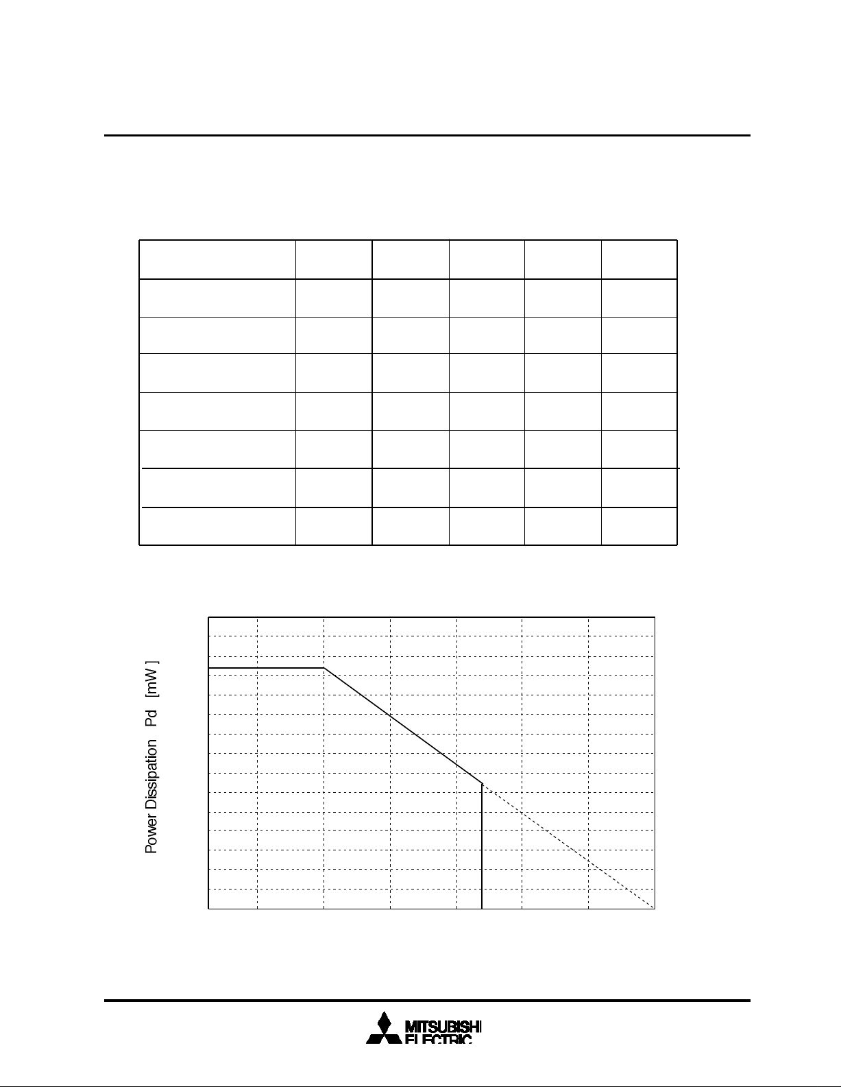
1.ABSOLUTE MAXIMUM RATING
(Ta = 25°C, Surge capacity=200pF)
Parameter
Supply voltage
Power dissipation
Operating temperature
Storage temperature
Recommended
operating voltage
Recommended operating
voltage range
Surge
Symbol
Vcc
Pd
Topr
Tstg
Vopr
Vopr'
Vsurge
Min.
-20
-40
11.5
±200
Fig.3 THERMAL DERATING
1500
Typ
-
-
-
-
-
-
-
12.0
-
-
Max
13.0
1237.6
+85
+150
-
12.5
-
Unit
V
mW
°C
°C
V
V
V
1237.6
1000
500
643.6
0
-20
0
25
50
85
75 100 125
150
Ambient Temperature Ta [ °C ]
( / 25 )
5
Page 6
MITSUBISHI <LINEAR IC>
PROVISINAL INFORMATION M52759SP
UNIFORMITY FOR CRT DISPLAY MONITOR
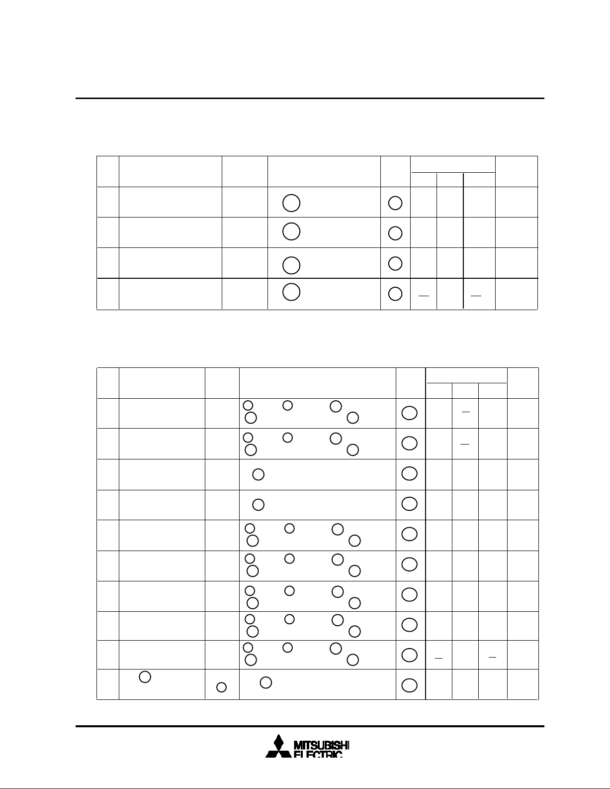
2.ELECTRICAL CHARACTERISTICS
(Ta=25°C, Vcc=12V, unless otherwise noted)
No
Parameter
Circuit current1
1
Circuit current2
2
Reference
3
voltage output
Reference voltage
4
temperature drift
HORIZONTAL BLOCK
5
6
Parameter
H-pulse low
input range
H-pulse high
input range
No
Symbol
ICCH
ICCV
VREF
DREF
Symbol
VIL
VIH
Test conditions
10 Measure
20 Measure
14 Measure
14 Measure
Test conditions
6 2.4V in 7 Measure 15 3.0V in
17 fH=96KHz H-pulse in 19 6.1V in
6 2.4V in 7 Measure 15 3.0V in
17 fH=96KHz H-pulse in 19 6.1V in
Pin
MIN TYP MAX
10
20
14
14
Pin
MIN TYP MAX
0.0 2.0 V
7
7
Limits
21.515.1 27.9
7.45.2 9.6
6.956.75 7.15 V
49
ppm/deg
Limit
s
3.0
VCC
-2.0
Unit
mA
mA
Unit
V
H-pulse low
7
input current
H-pulse high
8
input current
H parabola
9
width
H parabola
10
delay 1
H parabola
11
delay 2
H parabola
12
delay 3
Delay
13
temperature drift
Pin 15 input
14
current
IIL
IIH
TW µsec
TD1
TD2
TD3
DD
I 15
17 0V in,measure
17 5V in,measure
6 2.4V in 7 Measure 15 3.0V in
17 fH=96KHz H-pulse in 19 6.1V in
6 2.4V in 7 Measure 15 0V in
17 fH=96KHz H-pulse in 19 6.1V in
6 2.4V in 7 Measure 15 1.3V in
17 fH=96KHz H-pulse in 19 6.1V in
6 2.4V in 7 Measure 15 4.0V in
17 fH=96KHz H-pulse in 19 6.1V in
6 2.4V in 7 Measure 15 3.0V in
17 fH=96KHz H-pulse in 19 6.1V in
17 2.5V in,measure
17
-5.0
17
7
0.6 1.0
7
0.1 0.5
7
0.4
7
2.9 3.3
7
15
-5.0
-0.6 -0.1
0.0 1.0-1.0
0.8
0.3
0.8
0.6
3.1
0.08
-0.3
-0.1
( / 25 )
6
µA
µA
µsec
µsec
µsec
ns/deg
µA
Page 7
MITSUBISHI <LINEAR IC>
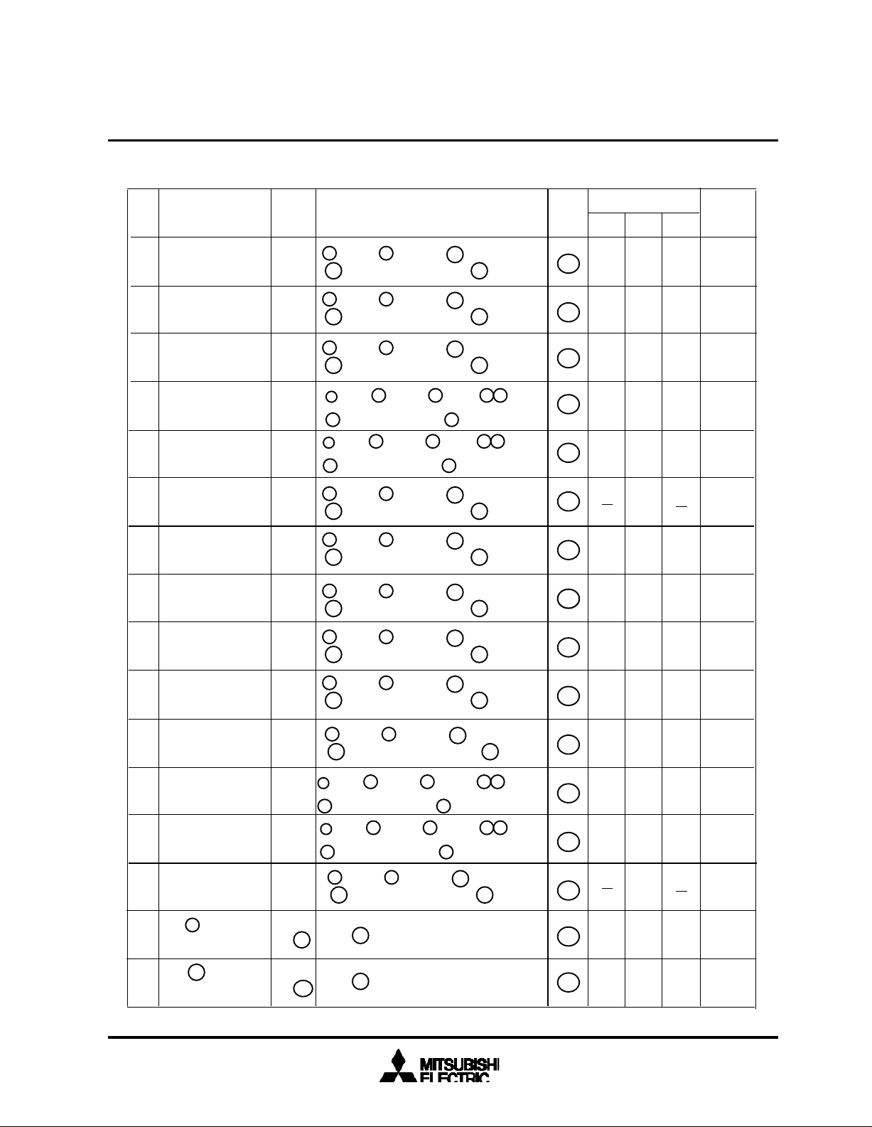
H para. unbalance
control1
H para. unbalance
control2
H para. unbalance
control3
H para. unbalance
Vcc. character1
PROVISINAL INFORMATION M52759SP
UNIFORMITY FOR CRT DISPLAY MONITOR
No
Parameter
15
16
17
18
H para. unbalance
19
Vcc. character2
H para. unbalance
20
temperature drift
H para. gain
21
control1
H para. gain
22
control2
Symbol
UHP1
UHP2
UHP3
VUHP1
VUHP2
DUHP
GHP1
GHP2
Test conditions
6 1.8V in 7 Measure 15 0V in
17 fH=96KHz H-pulse in 19 5.7V in
6 2.4V in 7 Measure 15 0V in
17 fH=96KHz H-pulse in 19 6.1V in
6 1.8V in 7 Measure 15 0V in
17 fH=96KHz H-pulse in 19 6.4V in
6 2.4V in 7 Measure 15 0V in 10 20 11.5V in
17 fH=96KHz H-pulse in 19 6.1V in
6 2.4V in 7 Measure 15 0V in 10 20 12.5V in
17 fH=96KHz H-pulse in 19 6.1V in
6 2.4V in 7 Measure 15 0V in
17 fH=96KHz H-pulse in 19 6.1V in
6 1.0V in 7 Measure 15 3.0V in
17 fH=96KHz H-pulse in 19 6.1V in
6 2.5V in 7 Measure 15 3.0V in
17 fH=96KHz H-pulse in 19 6.1V in
Pin
7
7
7
7
7
7
7
7
7
Limits
MIN TYP
-2.2
-2.6
0.1
0.5
2.1
1.7
-0.2
0.0
-0.2
0.0
-2.2
0.2
0.4
2.9
3.3
MAX
-1.8
0.9
2.5
0.2
0.2
0.6
3.7
Unit
V
V
V
V
V
mV /deg
Vp-p
Vp-p
H para. gain
23
control3
H para. freq.
24
characteristics1
H para. freq.
25
characteristics2
H para. Vcc.
26
characteristics1
H para. Vcc.
27
characteristics2
H para. size
28
temperature drift
Pin 6 input
29
current
Pin 19 input
30
current
GHP3
FHP1
FHP2
VVHP1
VVHP2
DHP
I 6
I 19
6 4.0V in 7 Measure 15 3.0V in
17 fH=96KHz H-pulse in 19 6.1V in
6 4.0V in 7 Measure 15 3.0V in
17 fH=24KHz H-pulse in 19 6.1V in
6 4.0V in 7 Measure 15 3.0V in
17 fH=120KHz H-pulse in 19 6.1V in
6 4.0V in 7 Measure 15 3.0V in 10 20 11.5V in
17 fH=96KHz H-pulse in 19 6.1V in
6 4.0V in 7 Measure 15 3.0V in 10 20 12.5V in
17 fH=96KHz H-pulse in 19 6.1V in
6 4.0V in 7 Measure 15 3.0V in
17 fH=96KHz H-pulse in 19 6.1V in
6 2.4V in,measure
19 6.1V in,measure
7
7
7
7
7
7
6
19
5.3
6.0
-0.2
0.0
0.0-0.2
0.0-0.2
0.0-0.2 0.2VV
-1.3
-0.3-5.0
0.3
0.1
6.7
0.2
0.2
0.2
-0.1
5.0
Vp-p
V
V
mV/deg
µA
µA
( / 25 )
7
Page 8
MITSUBISHI <LINEAR IC>
PROVISINAL INFORMATION M52759SP
UNIFORMITY FOR CRT DISPLAY MONITOR
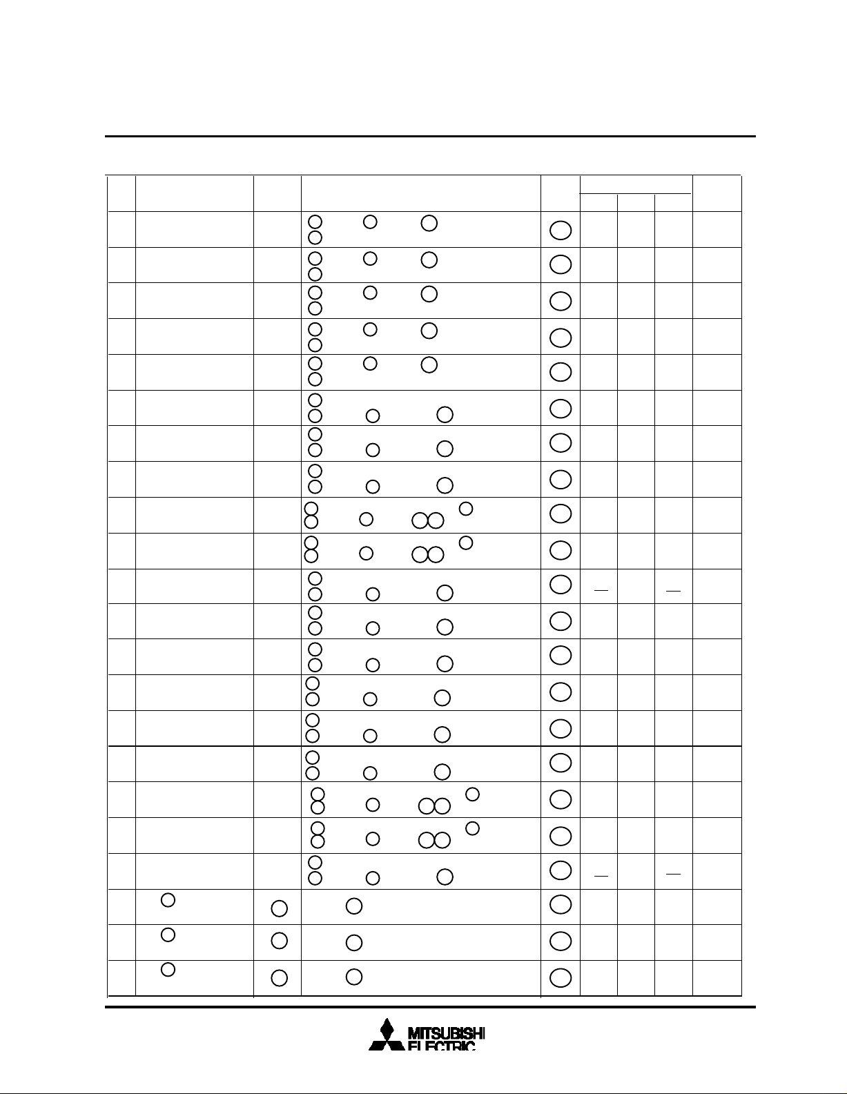
VERTICAL BLOCK
Parameter
No
V parabola
31
accuracy 1
V parabola
32
accuracy 2
V parabola
33
accuracy 3
V parabola
34
accuracy 4
V parabola
35
accuracy 5
V para. unbalance
36
control1
V para. unbalance
37
control2
V para. unbalance
38
control3
V unbalance. Vcc.
39
characteristics 1
V unbalance. Vcc.
40
characteristics 2
V unbalance.
41
temperature drift
V parabola
42
amplitude 1
V parabola
43
amplitude 2
V parabola
44
amplitude 3
V para. freq.
45
characteristics 1
V para. freq.
46
characteristics 2
V para. Vcc.
47
characteristics 1
V para. Vcc.
48
characteristics 2
V para.
49
temperature drift
Pin 2 input
50
current
Pin 3 input
51
current
Pin 5 input
52
current
Symbol
AVP1 V
AVP2
AVP3
AVP4
AVP5
UVP1
UVP2
UVP3
VUVP1
VUVP2
DUVP
GVP1 Vp-p
GVP2
GVP3
FVP1
FVP2
VVP1
VVP2
DVP
2 3.5V in 3 3.5V in 4 Measure
5 2.3V in
2 1.9V in 3 3.5V in 4 Measure
5 2.3V in
2 2.7V in 3 3.5V in 4 Measure
5 2.3V in
2 4.3V in 3 3.5V in 4 Measure
5 2.3V in
2 5.1V in 3 3.5V in 4 Measure
5 2.3V in
2 fv=70Hz, 3.2Vpp saw wave in
3 2.8V in 4 Measure 5 1.6V in
2 fv=70Hz, 3.2Vpp saw wave in
3 3.5V in 4 Measure 5 2.3V in
2 fv=70Hz, 3.2Vpp saw wave in
3 4.2V in 4 Measure 5 1.6V in
2 fv=70Hz, 3.2Vpp saw wave in 3 3.5V in
4 Measure 5 2.3V in 10 20 11.5V in
2 fv=70Hz, 3.2Vpp saw wave in 3 3.5V in
4 Measure 5 2.3V in 10 20 12.5V in
2 fv=70Hz, 3.2Vpp saw wave in
3 3.5V in 4 Measure 5 2.3V in
2 fv=70Hz, 3.2Vpp saw wave in
3 3.5V in 4 Measure 5 1.0V in
2 fv=70Hz, 3.2Vpp saw wave in
3 3.5V in 4 Measure 5 2.0V in
2 fv=70Hz, 3.2Vpp saw wave in
3 3.5V in 4 Measure 5 3.0V in
2 fv=50Hz, 3.2Vpp saw wave in
3 3.5V in 4 Measure 5 3.0V in
2 fv=185Hz, 3.2Vpp saw wave in
3 3.5V in 4 Measure 5 3.0V in
2 fv=70Hz, 3.2Vpp saw wave in 3 3.5V in
4 Measure 5 3.0V in 10 20 11.5V in
2 fv=70Hz, 3.2Vpp saw wave in 3 3.5V in
4 Measure 5 3.0V in 10 20 12.5V in
2 fv=70Hz, 3.2Vpp saw wave in
3 3.5V in 4 Measure 5 3.0V in
I 2
I 3
I 5
Test conditions
2 3.5V in,measure
3 3.5V in,measure
5 2.3V in,measure
Pin
4
4
4
4
4
4
4
4
4
4
4
4
4
4
4
4
4
4
4
2
3
5
Limits
MIN TYP MAX
5.0
4.5 5.5
2.5
3.0
3.5
20
25
30
20
25
30
90
100
110
-2.5
-2.8 -2.2
-0.3
2.2 2.8
0
2.5
0.3
0.1
0.5
0
0
0.3
2.1
2.4
2.7
4.7
4.2 5.2
-0.1
0.0
0.1
0.0-0.1 0.1
-2.2
-0.3-5.0 -0.1
-0.3-5.0 -0.1
-0.3-5.0 -0.1
Unit
%
%
%
mV/deg
Vp-p
Vp-p
mV/deg
µA
µA
µA
V
V
V
V
V0.0-0.1
V0.0-0.1 0.1
V
V
V0.0-0.1 0.1
V0.0-0.1 0.1
( / 25 )
8
Page 9

MITSUBISHI <LINEAR IC>
b
PROVISINAL INFORMATION M52759SP
UNIFORMITY FOR CRT DISPLAY MONITOR
Switch and Voltage Condition
No
1
2
3
4
5
6
7
8
9
10
11
12
13
14
15
16
17
18
19
20
21
22
23
Symbol
ICCH
ICCV
VREF
DREF
VIL
VIH
IIL
IIH
TW
TD1
TD2
TD3
DD
I 15
UHP1
UHP2
UHP3
VUHP1
VUHP2
DUHP
GHP1
GHP2
GHP3
Switch
SW2 SW6 SW10 SW15 SW17 SW19 SW20
SW3 SW5
a a a
a
baa
aba
b
b
a
a
b
a
b
b
a
a
Voltage
V2 V5 V6 V15 V17 V19Vcc
V3
12.0 3.5 2.5 2.4
11.5
12.5
12.0
3.5
1.8
2.4
1.8
2.4
1.0
2.5
4.0
[ V ]
3.0
0
1.3
4.0
3.0
0
3.0
0
-
0
5.0
-
0
-
6.1
5.7
6.1
6.4
6.1
24
FHP1
25
FHP2
26
27
28
29
30
VVHP1
VVHP2
DHP
I 6
I 19
b
a
11.5
12.5
12.0
-
2.4
( / 25 )
0
-
9
Page 10

MITSUBISHI <LINEAR IC>
PROVISINAL INFORMATION M52759SP
UNIFORMITY FOR CRT DISPLAY MONITOR
No
31
32
33
34
35
36
37
38
39
40
41
42
Symbol
AVP1
AVP2
AVP3
AVP4
AVP5
UVP1
UVP2
UVP3
VUVP1
VUVP2
DUVP
GVP1
Switch
SW2 SW6 SW10 SW15 SW17 SW19 SW20
SW3 SW5
a
a a a b a a
b
12.0
11.5
12.5
12.0
V2 V5 V6 V15 V17 V19Vcc
3.5
1.9
2.7
4.3
5.1
-
Voltage
V3
3.5
2.8
3.5
4.2
3.5
[ V ]
2.4 3.0 0 6.1
2.3
1.6
2.3
1.6
2.3
1.0
43
44
45
46
47
48
49
50
51
52
GVP2
GVP3
FVP1
FVP2
VVP1
VVP1
DVP
I 2
I 3
I 5
c
aab
aab
11.5
12.5
12.0
3.5
2.0
3.0
2.3
-
( / 25 )
10
Page 11

MITSUBISHI <LINEAR IC>
PROVISINAL INFORMATION M52759SP
UNIFORMITY FOR CRT DISPLAY MONITOR
Input Signal
PG
VTH=2.5V
(Input Signal to Pin 17 )
Pulse width above1 µsec
frequency 24 to96 to140KHz
5.0V Typ
0V Typ
SG
(Input Signal to Pin 2 )
The way to measure
No1.ICCH
No2.ICCV
No3.VREF
No4.VREF
No5.VIL
Measure the input current to Pin-10.
Measure the input current to Pin-20.
Measure the output voltage at Pin-14
Measure temperature drift of Pin-14 .(-20°C to 85°C )
Input Signal to Pin-17
Output Signal at Pin-7
frequency 50 to70 to185Hz
1.6
V
1.6
V
3.5V
5.0V
2.0V
Input horizontal pulse which low level is 2V in Pin-17 and confirm output horizontal
signal at Pin-7.
No6.VIH
Input Signal to Pin-17
Output Signal at Pin-7
Input horizontal pulse which high level is 3V in Pin-17 and
confirm
output horizontal signal at Pin-7.
( / 25 )
11
3.0V
0V
Page 12

MITSUBISHI <LINEAR IC>
PROVISINAL INFORMATION M52759SP
UNIFORMITY FOR CRT DISPLAY MONITOR
T
No9.TW
Input Signal to Pin-17
W
Measure the time width of retrace period at Pin-7.
No10.TD1 No11.TD2 No12.TD3
Input signal to Pin-17
TD1,TD2,
TD3
Output signal at Pin-7
Measure the delay time from rise time of input signal to start of retrace
period of output signal when the voltage of Pin-15 is 0V,1.3V,and 4V.
NO13.D D Measure the temperature drift of the delay time.(-20°C to 85°C )
NO14.I-15
Measure the input current to Pin-15 when the voltage of Pin-15 is 2.5V.
No15.UHP1 No16.UHP2 No17.UHP3
UHPS
Output signal at
UHP
UHPE
Pin-7
5.0V
0V
UHPS is defined as the voltage of parabola start point . UHPE is defined as
the voltage of parabola end point .UHP1 UHP2 UHP3 is defined as follows
UHP1 UHP2 UHP3 = UHPS - UHPE
Measure the unbalance of parabola waveform at Pin-4 when the voltage of
Pin-19 is 5.7V,6.1V,and 6.4V. Pin-6 is controled so that the amplitude of
parabola is 3Vp-p constant.
( / 25 )
12
Page 13

MITSUBISHI <LINEAR IC>
frequency of input signal is 24kHz ,the amplitude of parabola waveform
is defined as HP24KHZ.
When the supply voltage of Pin-10,20 is 12.5V,the amplitude of
parabola waveform at Pin-7 is defined as HP12.5V.
When the frequency of input signal in Pin-17 is 140kHz ,the amplitude of
parabola waveform at Pin-7 is defined as HP120KHZ.
PROVISINAL INFORMATION M52759SP
UNIFORMITY FOR CRT DISPLAY MONITOR
No18.VUHP1
No19.VUHP2
No20.DUHP
No21.GHP1
No22.GHP2
No23.GHP2
NO24.FHP1
When the supply voltage of Pin-10,20 is 11.5V,the unbalance
of parabola waveform at Pin-7 is defined as UHP11.5V.
VUHP1 = UHP2 - UHP11.5V
When the supply voltage of Pin-10,20 is 12.5V,the unbalance
of parabola waveform at Pin-7 is defined as UHP12.5V.
VUHP2 = UHP2 - UHP12.5V
Measure temperature drift of UHP2 . ( -20°C to 85°C )
Measure the amplitude of parabola waveform at Pin-7 and it is
defined as HP-6,1.0V
The amplitude of parabola waveform at Pin-7 is defined as
HP-6,2.5V.
The amplitude of parabola waveform at Pin-7 is defined
as HP-6,4.0V.
When the frequency of input signal in Pin-17 is 96kHz ,the amplitude of
parabola waveform at Pin-7 is defined as HP96KHZ. When the
NO25.FHP2
NO26.VVHP1
NO27.VVHP2
No28.DHP
No29.I-6
No30.I-19
FHP1 = HP96KHZ - HP24KHZ
FHP2 = HP96KHZ HP140KHZ
When the supply voltage of Pin-10,20 is 12.0V,the amplitude of
parabola waveform at Pin-7 is defined as HP12.0V. When the supply
voltage is 11.5V,the amplitude of parabola waveform is defined as
HP11.5V.
VVHP1 = HP12.0V- HP11.5V
VVHP2 = HP12.0V - HP12.5V
Measure the temperature drift of HP96KHz. (-20°C to 85°C )
Measure the input current to Pin-6 when voltage of Pin-6 is 2.4V.
Measure the input current to Pin-19 when voltage of Pin-19 is 6.1V.
( / 25 )
13
Page 14

MITSUBISHI <LINEAR IC>
PROVISINAL INFORMATION M52759SP
UNIFORMITY FOR CRT DISPLAY MONITOR
No31.AVP1
No32.AVP2
Measure the output voltage at Pin-4and it is defined as VP-2,3.5V.
The output voltage at Pin-4 is defined as VP-2,1.9V.
AVP2 = VP-2,1.9V - VP-2,3.5V
No33.AVP3
The output voltage at Pin-4 is defined as VP-2,2.7V.
VP-2,2.7V - VP-2,3.5V
AVP3 =
VP-2,1.9V - VP-2,3.5V
x 100 (%)
No34.AVP4 The output voltage at Pin-4 is defined as VP-2,4.3V.
AVP4 =
VP-2,4.3V - VP-2,3.5V
VP-2,1.9V - VP-2,3.5V
x 100 (%)
No35.AVP5 The output voltage at Pin-4 is defined as VP-2,5.1V.
VP-2,5.1V - VP-2,3.5V
AVP5 =
VP-2,1.9V - VP-2,3.5V
x 100 (%)
No36.UVP1 No37.UVP2 No38.UVP3
UVPS
Output signal at Pin-7
UVP
E
No39.VVP1
No40.VVP2
No41.DVP
UVPS is defined as the voltage of parabola start point . UVPE is defined as the
voltage of parabola end point .UVP1 UVP2 UVP3 is defined as follows
UVP1 UVP2 UVP3 = UVPS - UVPE
Measure the unbalance of parabola waveform at Pin-4 when the voltage of Pin-3
is 2.8V,3.5V,and 4.2V. Pin-5 is controled so that the amplitude of parabola is
3Vp-p constant
When the supply voltage of Pin-10,20 is 11.5V,the unbalance of
parabola waveform at Pin-4 is defined as UVP11.5V.
VUHP1 = UVP2 - UVP11.5V
When the supply voltage of Pin-10,20 is 12.5V,the unbalance of
parabola waveform at Pin-4 is defined as UVP12.5V.
VUVP2 = UVP2 - UVP12.5V
Measure temperature drift of UVP2 .(-20°C to 85°C )
( / 25 )
14
Page 15

MITSUBISHI <LINEAR IC>
PROVISINAL INFORMATION M52759SP
UNIFORMITY FOR CRT DISPLAY MONITOR
No42.GVP1 No43.GVP2
No44.GVP3
Measure the amplitude of parabola waveform at Pin-4 when the voltage
of Pin-5 is 1V,2V,and 3V.
No45.FVP1
When the frequency of input signal in Pin-2 is 70Hz ,the amplitude of
parabola waveform at Pin-4is defined as VP70Hz. When the frequency of
input signal is 50Hz ,the amplitude of parabola waveform is defined as
No46.FVP2
VP50Hz.
When the frequency of input signal in Pin-2 is185Hz
FVP1 = VP70Hz - VP50Hz
,the amplitude of parabola waveform at Pin-4 is defined as VP185Hz.
FVP2 = VP70Hz - VP185Hz
No47.VVP1
When the voltage of Pin-10,20 is 12.0V,the amplitude of parabola waveform
is defined as VP12.0V. When the voltage is 11.5V,the amplitude of parabola
waveform is defined as VP11.5V.
VVP1 = VP12.0V - VP11.5V
No48.VVP2
When the voltage of Pin-10,20 is 12.5V,the amplitude of parabola waveform
is defined as VP12.5V.
VVP2 = VP12.0V - VP12.5V
No49.DuVP Measure temperature drift of VP70Hz. (-20°C to 85°C)
No50.I-2
No51.I-3
No52.I-5
Measure the input current to Pin-2 when the voltage of Pin-2 is 3.5V.
Measure the input current to Pin-3when the voltage of Pin-3 is 3.5V.
Measure the input current to Pin-5when the voltage of Pin-5 is 2.4V.
( / 25 )
15
Page 16

MITSUBISHI <LINEAR IC>
PROVISINAL INFORMATION M52759SP
UNIFORMITY FOR CRT DISPLAY MONITOR
TEST CIRCUIT
33µF
+
0.01µF
0.01µF
+
1µF
6.8K
100pF
100pF
100pF
0.01µF
33µF
( / 25 )
16
Page 17

MITSUBISHI <LINEAR IC>
PROVISINAL INFORMATION M52759SP
UNIFORMITY FOR CRT DISPLAY MONITOR
3.TYPICAL CHARACTERISTICS
Note:This is not final
characteristics.
Horizontal Block
Delay control voltage vs Delay time
(µs)
3.5
3
2.5
2
1.5
1
0.5
0
0
Usable range
0.5 1.3
1 2 3 5
Usable
range
Usable range
4
Pin-17input
Delay time
Pin-7output
(V)
Pin-15 Delay control voltage
H unbarance control bias voltage vs H parabola unbarance
Pin-6 is controled as the amplitude
of parabola is 3Vp-p constant
(V)
2
Pin-7 output
1
0
-1
-2
5.7 5.9 6.3
Pin-19 H unbarance control bias voltage
6.1
6.5
(V)
( / 25 )
17
Page 18

MITSUBISHI <LINEAR IC>
Vertical Block
PROVISINAL INFORMATION M52759SP
UNIFORMITY FOR CRT DISPLAY MONITOR
H gain control voltage vs H parabola amplitude
(Vp-p)
5
Pin-19 = 6.1V
const.
(%)
0
0 1
2
Pin-6 H gain control voltage
V para DC output voltage ratio
100
75
50
25
3 4
(V)
Pin-3=3.5V const.
Pin-5=2.3V const.
Output ratio
Pin-4out - Pin-4out@Pin-4=3.5V
=
Pin-4out@Pin-2=1.9V - Pin-4out@Pin-2=3.5V
x100 (%)
0
1.9 2.7 3.5 4.3
Pin-2 input voltage
5.1
(V)
( / 25 )
18
Page 19

MITSUBISHI <LINEAR IC>
PROVISINAL INFORMATION M52759SP
UNIFORMITY FOR CRT DISPLAY MONITOR
V unbarance control bias voltage vs V parabola unbarance
Pin-5 is controled as the amplitude of
(V)
parabola is 3Vp-p constant
3
2
1
0
-1
Pin-4 output
-2
-3
2.5
3.0
3.5 4.0
4.5
(V)
Pin-3 V unbarance control bias voltage
V para amp gain control voltage vs output amplitude
(Vp-p)
5
Pin-2 3.2Vpp sawtooth wave
4
3
2
input
1
0
0 1 2 3 4
Pin-5 V para amp gain control voltage
(V)
( / 25 )
19
Page 20

MITSUBISHI <LINEAR IC>
234
9
IC
PROVISINAL INFORMATION M52759SP
UNIFORMITY FOR CRT DISPLAY MONITOR
APPLICATION EXAMPLE
12.0V
Tha total resistance is
above10KΩ.
H Pulse
V-Vcc
20
H bias
H-GND
input
VPH
111213141516171819
V-GND
1
3.2Vpp
Para.A
mp
V-Saw
input
X
2
Vbias
Vout
Buffer
H-Pulse
Delay
VGV
(V Gain)
5
VGH
(H Gain)
6
Vref
2
X
SW
Para.Amp
& Limiter
Buffer
7 8
Hout
H-SAW
Generator
2 Vpp
AGC DET
above10KΩ
1%
1%
above10KΩ
10
H-Vcc
V
H/V
Deflection
DAC
( / 25 )
20
Page 21

MITSUBISHI <LINEAR IC>
2.8 to
4.2V
PROVISINAL INFORMATION M52759SP
UNIFORMITY FOR CRT DISPLAY MONITOR
4.DESCRIPTION OF PIN
Pin NO
1
2 Vsawi
3 Vbias
4 Vout
5
Name
V-GND
VGV
DC
Voltage
3.5V
5V
(Bottom)
1.0 to
3.0V
Equivalent circuit of pin Remarks
GND of vertical block
V-Vcc
V-GND
V-Vcc
V-GND
V-Vcc
V-GND
V-Vcc
V-GND
50uA
1K
2
50uA
1K
3
200
4
1mA
50uA
1K
5
Vertical sawtooth wave
input pin.
Vertical parabola
unbarance control bias
voltage input pin.
Input voltage range is
2.8 to 4.2V
Vertical parabola wave
output pin.
Bottom voltage=5V(fixed)
Amplitude is possible to control
by pin-5
Vertical parabola wave
gain control voltage input
pin.Input voltage range is
1.0 to 3.0V.
Vbias
6 VGH
1.0 to
4.0V
H-Vcc
H-GND
50uA
1K
6
Horizontal parabola wave
gain control voltage input
pin.Input voltage range is
1.0 to 4.0V.
( / 25 )
21
Page 22

MITSUBISHI <LINEAR IC>
PROVISINAL INFORMATION M52759SP
UNIFORMITY FOR CRT DISPLAY MONITOR
Pin NO Name
7 Hout
8
Cret
9 Ctrc
DC
Voltage
2.4 to
9.2V
7.1V
(Top)
4.9V
(Bottom)
7.1V
(Top)
4.9V
(Bottom)
Equivalent circuit of pin Remarks
H-Vcc
H-GND
H-Vcc
H-GND
H-Vcc
H-GND
200
7
1mA
0.25mA
8
1.5K
37uA
9
2K 2K
510
60uA
70uA
horizontal parabola wave
output pin.
Amplitude is possible to
control by pin-6.
Connection pin of horizon
-tal retrace capacitor.
Recommended capacitance is 100pF.
Connection pin of horizon
-tal trace capacitor.
Recommended capacitance is 100pF.
7.1V
4.9V
7.1V
4.9V
10
H-Vcc
12.0V
11 CAGCr 2.5V
H-Vcc
H-GND
Vcc of horizontal
block.
1
1
1.5K
Connection pin of horizon
-tal sawtooth wave AGC
retrace capacitor.
Recommended capacitance is 0.01µF
( / 25 )
22
Page 23

MITSUBISHI <LINEAR IC>
PROVISINAL INFORMATION M52759SP
UNIFORMITY FOR CRT DISPLAY MONITOR
Pin NO Name
12 CAGC 4.0V
13 Vrefr 1.28V
14 Vrefo 7.0V
0 to 0.5V
15 VPH
1.34. to V
DC
Voltage
Equivalent circuit of pin Remarks
H-Vcc
Connection pin of horizon
-tal AGC capacitor.
Recommended capacitance is 1µF.
Connection pin of
reference current source
resister.
Recommended resistance
is 6.8KΩ.
Reference voltage output
for horizontal pulse delay
circuit.
Should be connect more
than 10kΩ external
resister.
Delay adjustment voltage
input pin of horizontal
pulse.Input voltage range
is 1.3 to 4.0V.At 0 to 0.5V,
delay is minimized.
(0.5 to 1.3V is unusable
range.)
H-GND
H-GND
H-Vcc
H-GND
H-Vcc
H-GND
12
H-Vcc
14
15
7.5K
1.5K
4K
13
10p
50uA
0.2mA
50uA
1K
16 Chpd
0V
(Bottom)
H-Vcc
16
H-GND
2K 2K
1K
Connection pin of horizon
50uA
-tal pulse delay timing
capacitor.Recommended
capacitance is 100pF.
H
0.5 to 5.0Vpp
0V
( / 25 )
23
Page 24

MITSUBISHI <LINEAR IC>
PROVISINAL INFORMATION M52759SP
UNIFORMITY FOR CRT DISPLAY MONITOR
Pin NO Name
17 HPin
18 H-GND
19 Hbias
20 V-Vcc
DC
Voltage
5.7 to
6.4V
12.0V
Equivalent circuit of pin Remarks
H-Vcc
Horizontal pulse input pin.
Low input level is less
than 2.0V,and high is 3.0
to 10V(at Vcc=12V).
GND of horizontal block
Horizontal parabolall
unbarance control
bias voltage input pin.Input
Voltage range is 5.7 to
6.4V.
Vcc of vertical block
H-GND
H-Vcc
H-GND
19
17
1K
50uA
1K
50K
1p
50uA
( / 25 )
24
Page 25

MITSUBISHI <LINEAR IC>
5. MARK
X X X X X X
M 5 2 7 5 9 SP
6. Material
Resin Epoxy resin
7. Factory of massproduction
FUKUOKA Fuctory
PROVISINAL INFORMATION M52759SP
UNIFORMITY FOR CRT DISPLAY MONITOR
Lot No.
TYPE No
Frame Copper alloy
Lead plating Solder plating
( / 25 )
25
 Loading...