

Page 1
MITSUBISHI ICs (Monitor)
M52755FP
WIDE BAND ANALOG SWITCH
DESCRIPTION
The M52755FP is a semiconductor integrated circuit for the
RGBHV interface. The device features switching signals input from
two types of image sources and outputting the signals to the CRT
display, etc. Synchronous signals, meeting a frequency band of
10kHz to 200kHz, are output at TTL. The frequency band of video
signals is 250MHz, acquiring high-resolution images, and are
optimum as an interface IC with high-resolution CRT display and
various new media.
FEATURES
•
Frequency band:RGB......................................................250MHz
HV.............................................10Hz to 200kHz
Input level:RGB.........................................................0.7V
HV TTL input.............................3.5V
•
Only the G channel is provided with sync-on video output.
•
The TTL format is adopted for HV output.
O-P
(both channel)
P-P
(typ.)
APPLICATION
Display monitor
RECOMMENDED OPERATING CONDITION
Supply voltage range........................................................4.5 to 5.5V
Rated supply voltage..................................................................5.0V
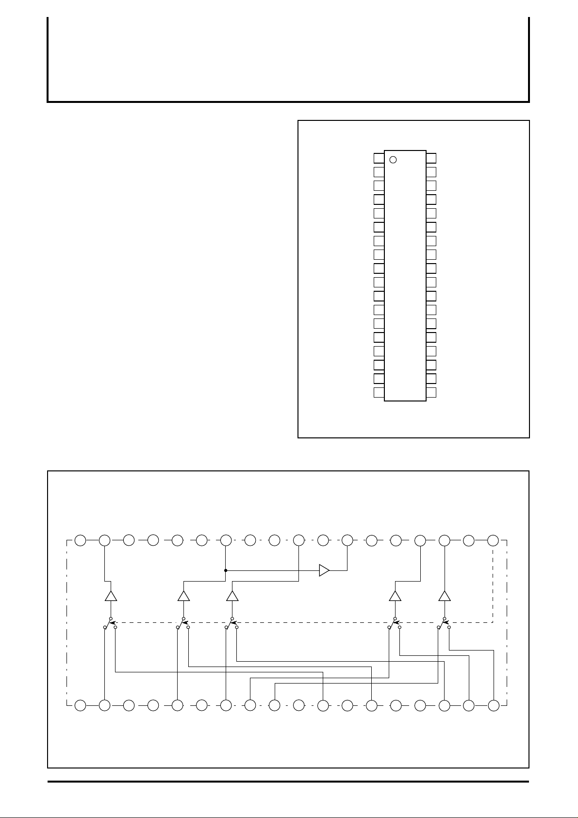
PIN CONFIGURATION (TOP VIEW)
V
INPUT1 (R)
V
INPUT1 (G)
V
INPUT1 (B)
INPUT1 (H)
INPUT1 (V)
INPUT2 (R)
INPUT2 (G)
INPUT2 (B)
INPUT2 (H)
INPUT2 (V)
1
CC1 (R) Vcc2 (R)
2
3
CC1 (G)
NC
4
CC1 (B)
7
8
GND
GND
13
NC
14
15 22
GND
16 21
17 20
18 19
36
35
34
33
325
316
30
M52755FP
29
289
2710
2611
2512
24
23
OUTPUT (R)
GND
NC
NC
Vcc
OUTPUT (G)
GND
Vcc
OUTPUT (B)
GND
OUTPUT (for sync on G)
CC
V
NC
OUTPUT (H)
OUTPUT (V)
GND
SWITCH
Outline 36P2R-A
2 (G)
2 (B)
NC : NO CONNECTION
BLOCK DIAGRAM
OUTPUT (R)
Vcc
2 (R) GND
36
1
V
CC1 (R)
GND
34
35
2
3
CC1 (G)
V
OUTPUT
OUTPUT (B) SWITCH
2 (B)
27
28
10
INPUT1 (V)
GNDV
30
INPUT1 (H)
GND
29
NC
32
Vcc2 (G)
OUTPUT (G) Vcc
31
6 8
CC1 (B)INPUT1 (R)
INPUT1 (B)INPUT1 (G)
NC
33
45 97
NC NC
(for sync on G)
26
INPUT2 (R)
25
GND
INPUT2 (G)
NC
V
CC GND
23
24
OUTPUT (V)
OUTPUT (H)
22
GND
21
INPUT2 (H)
19
20
181614131211
1715
INPUT2 (V)INPUT2 (B)
1
Page 2
°
°
±
− b − b − b − b − b − b − b − b − b −
− b − b − b − b − b − b − b − b − b −
− b − b − b − b − b − b − b − b − b −
− b − b − b − b − b − b − b − b − b −
b − b − b − b − b − b − b −
− b − b −
−
MITSUBISHI ICs (Monitor)
M52755FP
WIDE BAND ANALOG SWITCH
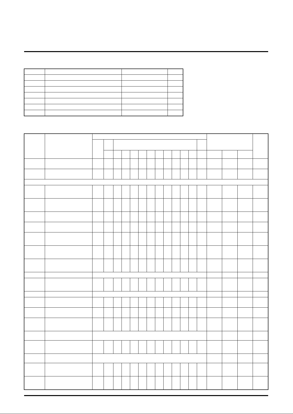
ABSOLUTE MAXIMUM RATINGS
(Ta=25 ° C)
Symbol Parameter Ratings Unit
V
CC
P
d
T
opr
T
stg
V
opr
V
opr’
Surge Electrostatic discharge
ELECTRICAL CHARACTERISTICS
Supply voltage 7.0 V
Power dissipation 1603 mW
Ambient temperature -20 to +85
Storage temperature -40 to +150
Recommended supply voltage 5.0 V
Recommended supply voltage range 4.5 to 5.5 V
200 V
(V
CC
=5V , Ta=25 ° C, unless otherwise noted)
C
C
Test conditions
Symbol Parameter
I
CC1
CC2
I
Circuit current1
(no signal)
Circuit current2
(no signal)
V
Test
(V)
point
(s)
V
A5
A5
CC
CC
SW2
Rin1
b
−
b
−
SW4
Gin1
b
−
b
−
SW6
Bin1
b
−
b
−
Input SW
SW10
SW12
SW7
Hin1
b
−
b
−
SW8
Vin1
b
−
b
−
Rin2
Gin2
b
−
b
−
SW14
b
−
b
−
Bin2
b
−
b
−
SW15
Hin2
b
−
b
−
SW16
Vin2
b
−
b
−
SW17
Switch
b
GND
a
OPEN
Limits
Min. Typ. Max.
46 66 86 mA
46 66 86 mA
(RGB SW)
T.P.31
DC1
V
DC2
V
V
DC3
DC4
V
Vi
max1
Vi
max2
Output DC voltage1
Output DC voltage2
Output DC voltage3
Output DC voltage4
Maximum allowable
input1
Maximum allowable
input2
GV1 Voltage gain1
V1 Relative voltage gain1 Relative to measured values above -0.4 0 0.4 dB
∆G
V2 Voltage gain2
G
V2 Relative voltage gain2 Relative to measured values above -0.4 0 0.4 dB
∆G
V3 Voltage gain3
G
V4 Voltage gain4
G
FC1
C1
∆F
C2
F
∆FC2
FC3
C4
F
Freq. characteristic1
(100MHz)
Relative Freq.
characteristic1 (100MHz)
Freq. characteristic2
(100MHz)
Relative Freq.
characteristic2 (100MHz)
Freq. characteristic3
(250MHz)
Freq. characteristic4
(250MHz)
T.P.28
T.P.25
T.P.31
T.P.28
T.P.25
T.P.23
T.P.23
T.P.2
T.P.4
T.P.6
T.P.10
T.P.12
T.P.14
T.P.31
T.P.28
T.P.25
T.P.31
T.P.28
T.P.25
T.P.23
T.P.23
T.P.31
T.P.28
T.P.25
T.P.31
T.P.28
T.P.25
T.P.31
T.P.28
T.P.25
T.P.31
T.P.28
T.P.25
b
5
b
5
b
5
b
5
abb
bab
5
SG1
5
abb
5
SG2
5
5
5
abb
5
SG4
bba
SG1
SG1
b
bab
bba
SG2
SG2
b−b−b−b−b
b
−
b−b−b−b−b−b−b−b−b
a
SG2
b−b−b−b−b−b
bab
bba
SG4
SG4
b−b
abb
bab
SG1
SG1
−
bba
SG1
b−b−a
b−b−b−b−b−b−b−b
bab
abb
SG2
SG2
−
a
SG2
−
b−b
bba
SG2
b−b−b−a
b−b−b−b−b−b−b−b
b
1.85 2.05 2.25 V
GND
a
1.85 2.05 2.25 V
OPEN
b
0.75 1.15 1.55 V
GND
a
0.75 1.15 1.55 V
OPEN
b
2.0 2.4
GND
2.0 2.4 − VP-P
OPEN
0.3 0.9 1.5 dB
GND
a
0.3 0.9 1.5 dB
OPEN
−
-0.4 0.2 0.8 dB
GND
-0.4 0.2 0.8 dB
OPEN
-1.0 0 1.0 dB
GND
Relative to measured values above -1.0 0 1.0 dB
b−b−b−b−b
5
bab
abb
SG4
SG4
−
bba
SG4
b−b−a
OPEN
-1.0 0 1.0 dB
Relative to measured values above -1.0 0 1.0 dB
abb
5
5
bab
SG5
SG5
b−b−b−b−b
b−b−b−b−b−b−b−b
bba
SG5
bab
SG5
bba
SG5
abb
SG5
−
GND
b−b−a
OPEN
-3.0 -1.5 1.0 dB
-3.0 -1.5 1.0 dB
Unit
P-P
V
2
Page 3
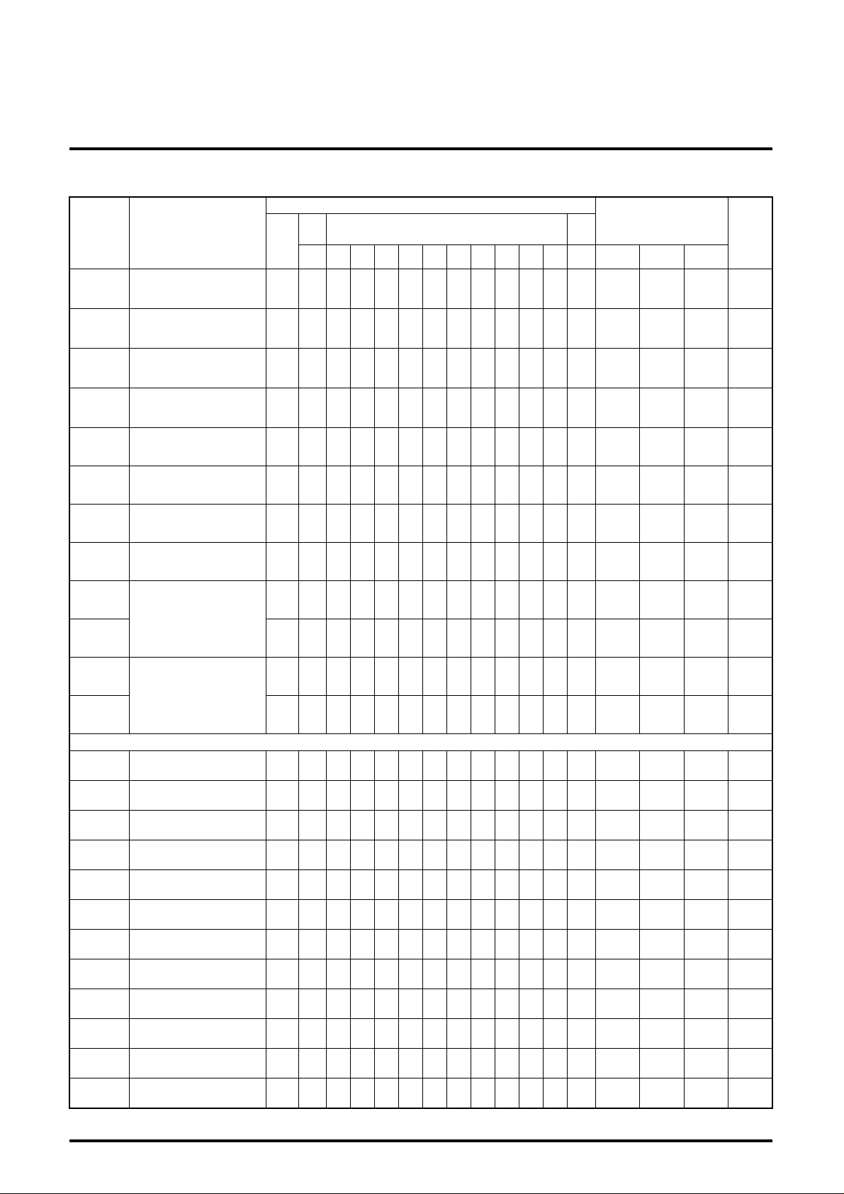
ELECTRICAL CHARACTERISTICS (cont.)
V
CC
Symbol Parameter
C.T.I.1
C.T.I.2
C.T.I.3
C.T.I.4
C.T.C.1
C.T.C.2
C.T.C.3
C.T.C.4
Crosstalk between two
inputs1 (10MHz)
Crosstalk between two
inputs2 (10MHz)
Crosstalk between two
inputs3 (100MHz)
Crosstalk between two
inputs4 (100MHz)
Crosstalk between
channels1 (10MHz)
Crosstalk between
channels2 (10MHz)
Crosstalk between
channels3 (100MHz)
Crosstalk between
channels4 (100MHz)
Tr1
Pulse characteristic1
Tf1
Tr2
Pulse characteristic2
Tf2
(HV SW)
VoH1
VoH2
VoL1
VoL2
Vith1
Vith2
High level
output voltage1
High level
output voltage2
Low level
output voltage1
Low level
output voltage2
Input selectional
voltage1
Input selectional
voltage2
Trd1 Rising delay time1
Trd2 Rising delay time2
Tfd1 Falling delay time1
Tfd2 Falling delay time2
Vsth1
Vsth2
Switching selectional
voltage1
Switching selectional
voltage2
Test
point
(s)
T.P.31
T.P.28
T.P.25
T.P.31
T.P.28
T.P.25
T.P.31
T.P.28
T.P.25
T.P.31
T.P.28
T.P.25
T.P.31
T.P.28
T.P.25
T.P.31
T.P.28
T.P.25
T.P.31
T.P.28
T.P.25
T.P.31
T.P.28
T.P.25
T.P.31
T.P.28
T.P.25
T.P.31
T.P.28
T.P.25
T.P.31
T.P.28
T.P.25
T.P.31
T.P.28
T.P.25
T.P.19
T.P.20
T.P.19
T.P.20
T.P.19
T.P.20
T.P.19
T.P.20
T.P.7
T.P.8
T.P.15
T.P.16
T.P.19
T.P.20
T.P.19
T.P.20
T.P.19
T.P.20
T.P.19
T.P.20
T.P.17
T.P.17
V
(V)
CC
5
5
5
5
5
5
5
5
5
5
5
5
5
5
5
5
5
5
5
5
5
5
5
5
WIDE BAND ANALOG SWITCH
Test conditions
Input SW
SW10
SW12
SW14
SW15
−
−
−
−
SW16
Hin2
Vin2
−
b−b
−
−
b−b
−
b−b
−
b−b
−
b−b
−
b−b
−
c
5.0Vc5.0V
c
VariablecVariable
a
SG7aSG7
a
SG7aSG7
−
SW2
SW4
SW6
SW7
SW8
Rin2
Gin2
bab
SG3
bab
SG4
bab
SG3
bab
SG4
Bin2
bba
SG3
bba
SG4
bba
SG3
bba
SG4
Rin1
Gin1
Bin1
Hin1
abb
SG3
bab
SG3
b−b−b−b−b−b−b
bba
SG3
b−b−b−b−b
abb
SG4
bab
SG4
b−b−b−b−b−b−b
bba
SG4
b−b−b−b−b
abb
SG3
bab
SG3
b−b−b−b−b−b−b−b
bba
SG3
b−b−b−b−b
abb
SG4
bab
SG4
b−b−b−b−b−b−b−b
bba
SG4
b−b−b−b−b
a
SG6aSG6aSG6
a
SG6aSG6aSG6
b−b−b−b−b−b−b−b
b−b−b−b−b−b−b−b
b−b−b−b−b
b−b−b−b−b
b−b−b
−
c
5.0Vc5.0V
Vin1
abb
SG3
−
abb
SG4
−
abb
SG3
−
abb
SG4
−
a
SG6aSG6aSG6
−
a
SG6aSG6aSG6
−
b−b−b−b−b−b
b−b−b−b−b−b−b−b
b−b−b−c0Vc0Vb−b−b−b−b−b
b−b−b−b−b−b−b−b−c0Vc0Va
b−b−b
−
c
VariablecVariable
b−b−b−b−b−b
b−b−b−b−b−b−b−b
b−b−b
−
a
SG7aSG7
b−b−b−b−b−b
b−b−b−b−b−b−b−b
b−b−b
−
a
SG7aSG7
b−b−b−b−b−b
b−b−b−b−b−b−b−b
a
SG1aSG1aSG1aSG7aSG7
b−b−b−b−b
b−b−b−b−b
a
SG1aSG1aSG1aSG7aSG7
−
MITSUBISHI ICs (Monitor)
M52755FP
Limits
SW17
Min. Typ. Max.
Switch
GND
OPEN
GND
OPEN
GND
OPEN
GND
OPEN
GND
OPEN
GND
OPEN
GND
GND
OPEN
OPEN
GND
OPEN
GND
OPEN
GND
OPEN
GND
OPEN
GND
OPEN
− -60 -50 dB
↓
− -60 -50 dB
↓
− -40 -35 dB
↓
− -40 -35 dB
↓
− -50 -40 dB
a
− -50 -40 dB
− -30 -25 dB
a
− -30 -25 dB
− 1.6 2.5 nsec
− 1.6 2.5 nsec
a
− 1.6 2.5 nsec
a
− 1.6 2.5 nsec
4.5 5.0 − V
a
4.5 5.0 − V
− 0.2 0.5 V
− 0.2 0.5 V
2.0 2.5 3.0 V
a
2.0 2.5 3.0 V
− 100 150 nsec
a
− 100 150 nsec
− 50 100 nsec
a
− 50 100 nsec
c 0.5 1.5 2.0 V
c 0.5 1.5 2.0 V
Unit
3
Page 4

MITSUBISHI ICs (Monitor)
M52755FP
WIDE BAND ANALOG SWITCH
ELECTRICAL CHARACTERISTICS TEST METHOD
It omits the SW.No accorded with signal input pin because it is
already written in Table.
SW A, SW1, SW3, SW5 is in side a if there is not defined specially.
CC1, ICC2 Circuit current (no signal)
I
The condition is shown as Table 1. Set SW19 to GND (or OPEN)
and SW A to side b, measure the current by current meter A. The
current is as I
DC1, VDC2 Output DC voltage
V
Set SW19 to GND (or OPEN), measure the DC voltage of T.P.31
(T.P.28, T.P.25) when there is no signal input. The DC voltage is as
V
DC1 (or VDC2).
VDC3, VDC4 Output DC voltage
Measure the DC voltage of T.P.23 same as note2, the DC voltage is
as VDC3 (or VDC4).
Vimax1, Vimax2 Maximum allowable input
Set SW19 to GND, SG1 as the input signal of Pin 2. Rising up the
amplitude of SG1 slowly, read the amplitude of input signal when
the output waveform is distorted. The amplitude is as Vimax1. And
measure Vimax1 when SG2 as the input signal of Pin 5, Pin 7 in
same way. Next, set SW to OPEN, measure Vimax2 when SG2 as
the input signal of Pin11, 13, 16.
GV1, ∆GV1, GV2, ∆GV2
1. The condition is shown as Table.
2. Set SW19 to GND, SG2 as the input signal of Pin 2. At this time,
read the amplitude output from T.P 31. The amplitude is as VOR1.
3. Voltage gain GV1 is
4. The method as same as 2 and 3, measure the voltage gain G
when SG2 as the input signal of Pin 5, 7.
5. The difference of each channel relative voltage gain is as ∆GV1.
6. Set SW19 to OPEN, measure GV2, ∆GV12 in the same way.
GV3, GV4, V oltage gain
1. The condition is shown as table. This test is by active probe.
2. Measure the amplitude output from T.P.23.
3. Measure the GV3, GV4 by the same way as GV1, ∆GV1, GV2,
∆GV2.
FC1, ∆FC1, FC2, ∆FC2
1. The condition is shown as table. This test is by active probe.
2. Set SW19 to GND, SG2 as the input signal of Pin 2. Measure the
amplitude output from T.P.31. The amplitude is as VOR1. By the
same way, measure the output when SG4 is as input signal of
Pin 2, the output is as VOR2.
CC1 (ICC2).
V1= 20 LOG
G
OR1 [VP-P]
V
0.7 [V
P-P]
[dB]
V1
3. The frequency characteristic FC1 is
OR2 [VP-P]
F
C1= 20 LOG
V
OR1 [VP-P]
V
4. The method as same as 2 and 3, measure the frequency F
[dB]
C1
when input signal to Pin 5, 7.
5. The difference between of each channel frequency characteristic
is as ∆FC1.
6. Set SW19 to OPEN, measure FC2, ∆FC2.
C3, FC4 Freq. characteristic
F
By the same way as Note7 measure the F
C3, FC4 when SG5 of
input signal.
C.T.I.1, C.T.I.2 Crosstalk between two input
1. The condition is shown as Table. This test is by active prove.
2. Set SW19 to GND, SG3 as the input signal of Pin 2. Measure the
amplitude output from T.P.31. The amplitude is as VOR3.
3. Set SW19 to OPEN, measure the amplitude output from T.P.31.
The amplitude is as VOR3'.
4. The crosstalk between two inputs C.T.I.1 is
C.T.I.1= 20 LOG
OR3' [VP-P]
VOR3 [VP-P]
[dB]
V
5. By the same way, measure the crosstalk between two inputs
when SG3 as the input signal of Pin 5, Pin 7.
6. Next, set SW19 to OPEN, SG3 as the input signal of Pin 11,
measure the amplitude output from T.P.31. Theamplitude is as
V
OR4.
7. Set SW19 to GND, measure the amplitude output from T.P.31.
The amplitude is as VOR4'.
8. The crosstalk between two inputs C.T.I.2 is
C.T.I.2= 20 LOG
V
OR4 [VP-P]
V
[dB]
OR4' [VP-P]
9. By the same way, measure the crosstalk between channels
when SG3 as the input signal of Pin 13,16.
C.T.I.3, C.T.I.4 Crosstalk between two input
Set SG4 as the input signal, and then the same method as table,
measure C.T.I.3, C.T.I.4.
C.T.C.1, C.T.C.2 Crosstalk between channel
1. The condition is as Table. This test is by active prove.
2. Set SW19 to GND, SG3 as the input signal of Pin 2. Measure the
amplitude output from T.P.31. The amplitude is as V
OR5.
3. Next, measure T.P.28, T.P.25 in the same state, and the
amplitude is as VOG5, V OB5.
4. The crosstalk between channels C.T.C.1 is
OG5 or VOB5
C.T.C.1= 20 LOG
V
OR5
V
[dB]
4
Page 5

MITSUBISHI ICs (Monitor)
M52755FP
WIDE BAND ANALOG SWITCH
5. Measure the crosstalk between channels when SG3 is as the
input signal of Pin 5, Pin 7.
6. Next, set SW19 to OPEN, SG3 as the input signal of Pin11,
measure the amplitude output from T.P.31. The amplitude is as
VOR6.
7. Next, measure the amplitude output from T.P.28, T.P.25 in the
same state. The amplitude is as VOG6, VOB6.
8. The crosstalk between channels C.T.C.2 is
C.T.C.2= 20 LOG
OG6 or VOB6
OR6
V
[dB]
V
9. By the same way, measure the crosstalk between channels
when input signal to Pin13, 16.
C.T.C.3, C.T.C.4 Crosstalk between channel
Set SG4 as the input signal, and the same method as table,
measure C.T.C.3, C.T.C.4.
Tr1, Tf1, T r2, Tf2 Pulse characteristic
1. The condition is as Table. Set SW19 to GND (or OPEN).
2. The rising of 10% to 90% for input pulse is Tri, the falling of
10% to 90% for input pulse is Tfi.
3. Next, the rising of 10% to 90% for output pulse is Tro, the falling
of 10% to 90% for output pulse is Tfo.
4. The pulse characteristic Tr1, Tf1 ( Tr2, Tf2 ) is
VoL1, VoL2 Low level output voltage
The condition is as Table. Set SW19 to GND (OPEN), input 0V at
input terminal. Measure the output voltage, the voltage is as VoL1
(VoL2).
Vith1, Vith2 Input selectional voltage
The condition is as table. Set SW19 to GND (OPEN), increasing
gradually the voltage of input terminal from 0V, measure the voltage
of input terminal when output terminal is 4.5V. The input voltage is
as Vith1 (Vith 2).
Trd1, Trd2 Rising delay time
Tfd1, Tfd2 Falling delay time
The condition is as table. Set SW19 to GND (OPEN), SG7 is as the
input signal of input terminal, measure the waveform of output. Rising delay time is as Trd1 (Trd2). Falling delay time is as Tfd1 (Tfd2).
Reference to the Fig. as shown below.
50%
SG7
Output waveform
TfdTrd
50%
0%
100%
Tr
Tf
90%
10%
Tr1 (Tr2)=√(Tro)2 - (Tri)2 (nsec)
2
Tf1 (Tf2)=√(Tfo)
- (Tfi)2 (nsec)
VoH1, VoH2 High level output voltage
The condition is as Table. Set SW19 to GND (OPEN), input 5V at
input terminal. Measure the output voltage, the voltage is as V
OH1
(VOH2).
Vsth1, Vsth2 Switching selectional voltage
1. The condition is as table. SG1 is as the input signal of Pin 2,
Pin5, Pin7, and SG7 is as the input signal of Pin8, Pin9. There is
no input at another pins.
2. Input 0V at Pin19, confirm that there are signals output from
T .P.19, T .P.20, T.P.23, T .P.25, T.P .28, T.P.31.
3. Increase gradually the voltage of terminal Pin19. Read the
voltage when there is no signal output from the terminals listed
as above. The voltage is as Vsth1.
4. SG1 as the input signal of Pin11, Pin13, Pin16, and SG7 as the
input signal of Pin17, Pin18. There is no input at another pins.
5. Inputs 5V at Pin19, confirm that there is no signal output from
T .P.19, T.P.20, T .P.23, T.P .25, T.P.28, T .P.31.
6. Decreasing gradually the voltage of terminal Pin 19. Read the
voltage when there are signals output from the terminals listed
as above. The voltage is as Vsth2.
5
Page 6

INPUT SIGNAL
SG No. Signals
Sine wave (f=60kHz, 0.7VP-P, amplitude variable)
MITSUBISHI ICs (Monitor)
M52755FP
WIDE BAND ANALOG SWITCH
SG1
SG2 Sine wave (f=1MHz, amplitude 0.7V
P-P)
SG3 Sine wave (f=10MHz, amplitude 0.7VP-P)
SG4 Sine wave (f=100MHz, amplitude 0.7VP-P)
SG5 Sine wave (f=250MHz, amplitude 0.7VP-P)
Pulse with amplitude 0.7VP-P (f=60kHz, duty80%)
SG6
Square wave (Amplitude 5.0V
0.7VP-P
O-P TTL, f=60kHz, duty50%)
SG7
NOTE HOW TO USE THIS IC
1. R, G, B input signal is 0.7VP-P of standard video signal.
2. H, V input is 5.0V TTL type.
3. Input signal with sufficient low inpedance to input terminal.
4. The terminal of H, V output pin are shown as Fig.1. It is possible
to reduce rise time by insert the resister between Vcc line and H, V
output Pin, but set the value of resister in order that the current is
under 7.5mA. Setting the value of R is more than 2kΩ as shown in
Fig.1.
5V 5V
0.7VP-P(amplitude variable)
5V
0V
6. Switch (Pin 17) can be changed when this terminal is GND or
OPEN
When GND : Signal output from input 1
When OPEN: Signal output from input 2
When the switch is being used as Fig.3
0 to 0.5V : Signal output from input 1
2 to 5V : Signal output from input 2
It is not allowable to set voltage higher than V
17
CC.
Fig.3
1kΩ
1<7.5mA
R
Fig.1
5. The terminal of R,G,B output pin (Pin 25, 28, 31). It is possible to
add a pull-up resister according as drive ability. but set the value of
resister in order that the current is under 10mA. Setting the value of
R is more than 500Ω as shown in Fig.2.
5V
1<10mA
50Ω
430Ω
R
Fig.2
NOTICE OF MAKING PRINTED CIRCUIT BOARD.
Please notice following as shown below. It will maybe cause
something oscillation because of the P.C.B. layout of the wide band
analog switch.
⋅ The distance between resister and output pin is as short as
possible when insert a output pull-down resister.
⋅ The capitance of output terminal as small as possible.
⋅ Set the capitance between Vcc and GND near the pins if possible.
⋅ Using stable power-source (if possible the separated power-
source will be better).
⋅ It will reduce the oscillation when add a resister that is tens of
ohms between output pin and next stage.
⋅ Assign an area as large as possible for grounding.
6
Page 7

TEST CIRCUIT
MITSUBISHI ICs (Monitor)
M52755FP
WIDE BAND ANALOG SWITCH
a
VCC5V
A
SWA
0.01µ
0.01µ
b
0.01µ
0.01µ
SW2
47µ
TP35
R
35 34
213
TP2
0.01µ
47µ
100µ
a
b
0.01µ
3136 30 29 28 27 26 25 24
3233
45
TP5
47µ 47µ
0.01µ
a
0.01µ
100µ
b
67
TP7 TP9
0.01µ
SW7SW5
a
TP30
G
b
TP25
GOUT TP22HTP21
(for sync on G)
0.01µ
47µ
23 22
V
21 20
0.01µ
TP27
B
M52755FP
89
TP8
100µ
SW8 SW9 SW18SW17
a
a
c
bb
10 11
0.01µ
c
TP11
a
100µ
b
12 13
TP13
0.01µ
a
100µ
b
14 15
TP16
0.01µ
SW16SW13SW11
a
TP17
100µ
a
b
1716
TP18
c
b
SW19
19
18
a
b
OPEN
a
b
c
c
SG1
SG2
SG3
SG4
SG5
SG6
SG7
Units Resistance : Ω
Capacitance : F
7
Page 8

TYPICAL CHARACTERISTICS
3 to 5V
0V
THERMAL DERATING (MAXIMUM RATING)
1250
1068
1000
750
500
250
POWER DISSIPATION Pd (mW)
MITSUBISHI ICs (Monitor)
M52755FP
WIDE BAND ANALOG SWITCH
0 25 50 75 100 125
AMBIENT TEMPERATURE Ta (°C)
85
150-20
DESCRIPTION OF PIN
Pin No. Name DC voltage (V ) Peripheral circuit of pins Remarks
1
3
6
2
5
7
8
9
VCC1 (R)
VCC1 (G)
VCC1 (B)
Input1 (R)
Input1 (G)
Input1 (B)
Input1 (H)
Input1 (V)
5.0 −
800
1.5
2.59mA
−
620
Input signal with low
impedance.
2.2V
Input pulse between 3V
and 5V.
10, 12, 15, 20,
26, 29, 34
0.2mA
GND GND −
8
Page 9

MITSUBISHI ICs (Monitor)
3 to 5V
0V
M52755FP
WIDE BAND ANALOG SWITCH
DESCRIPTION OF PIN (cont.)
Pin No. Name DC voltage (V ) Peripheral circuit of pins Remarks
800
11
13
16
17
18
Input2 (R)
Input2 (G)
Input2 (B)
Input2 (H)
Input2 (V)
1.5
19 Switch 2.6
Input signal with low
impedance.
2.2V
620
2.59mA
Input pulse between 3V
and 5V.
−
0.2mA
10k
12k
13k
7.3k
2.3V
Switch by OPEN and
GND.
4, 14, 23,
9
21
22
24
32, 33
25
27
30
35
28
31
36
Output (V)
Output (H)
CC
V
(H, V , Switch)
−
5 −
1k
Output impedance is
built-in.
NC −−
Output
(Sync onG)
Output (B)
Output (G)
Output (R)
1.15
2.05
50
430
25, 28, 31
50
500
Output impedance is
built-in.
23
VCC2 (B)
VCC2 (G)
5 −
VCC2 (R)
 Loading...