

Page 1
DISCRIPTION
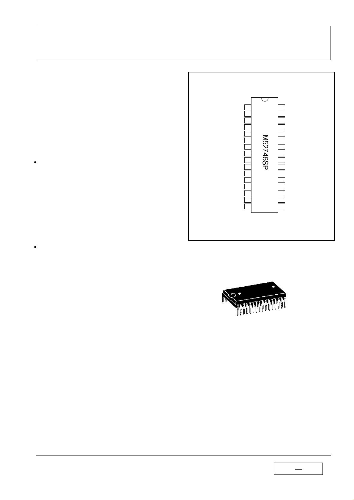
PIN CONFIGURATION
NC
M52746SP is Semiconductor Integrated Circuit
for CRT Display Monitor.
It includes OSD Blanking,OSD Mixing,Retrace
Blanking,Wide Band Amplifre,Brightness Control.
Main/Sub Contrast and OSD AdjustFunction can be
controlled by I2C Bus.
FEATURES
Frequency Band Width: RGB 200 MHz (at -3dB)
OSD 80 MHz
Input : RGB 0.7 Vp-p (Typ)
OSD light 4 Vp-p minimum (positive)
OSD harf 2.5Vp-p minimum (positive)
3.0Vp-p maximum (positive)
BLK(for OSD) 3 Vp-p minimum (positive)
Retrace BLK 3 Vp-p minimum (positive)
Output : RGB 5.5 Vp-p (maximum)
OSD 5 Vp-p (maximum)
MITSUBISHI< LINEAR IC >
M52746SP
BUS CONTROLLED 3CH VIDEO PRE-AMP FOR CRT DISPLAY MONITOR
Brightness
OSD IN (R)
OSD IN (B)
OSD IN (G)
OSD BLK IN
INPUT (R)
VCC 12V
INPUT (B)
GND
INPUT (G)
VCC 12V
INPUT(SOG)
SOG Sep OUT
Clamp Pulse IN
1 32
2 31
3 30
4 29
5
6
7
8
9 24
10 23
11
12
13 20
14 19
15
16
Outside Package: 32P4B
VCC 12V (R)
OUTPUT(R)
GND(R)
VCC 12V (B)
28
OUTPUT(B)
27
GND(B)
26
GND
25
VCC 12V (G)
OUTPUT(G)
GND(G)
22
Retrace BLK IN
21
SDA
SCL
GND
18
ABL IN
17
VCC 5V
Main Contrast and Sub Contrast can be controlled by I2C
Bus.
STRUCTURE
Bipola Silicon Monolisic IC
APPLICATION
CRT Display Monitor
RECOMMENDED OPERATING CONDITIONS
Supply Voltage Range 11.5V~12.5V(V7,V12,V25,V29,V32)
4.5V~4.4V(V17)
Rated Supply Voltage 12.0V(V7,V12,V25,V29,V32)
5.0V(V17)
MAJOR SPECIFICATION
Bus Controlled 3ch Video Pre-Amp with OSD Mixing Function
32 pin plastic SDIP
MITSUBISHI
1
25
Page 2
MITSUBISHI< LINEAR IC >
BUS CONTROLLED 3CH VIDEO PRE-AMP FOR CRT DISPLAY MONITOR
Absolute Maximum Rating (Ambient temperature: 25 C)
Parameter Symbol Rating Unit
M52746SP
Supply voltage 12
Supply voltage 5
Power dissipation
Ambient temperature
Storage temperature
Recommended supply 12
Recommended supply 5
voltage range 12
voltage range 5
Case temperature
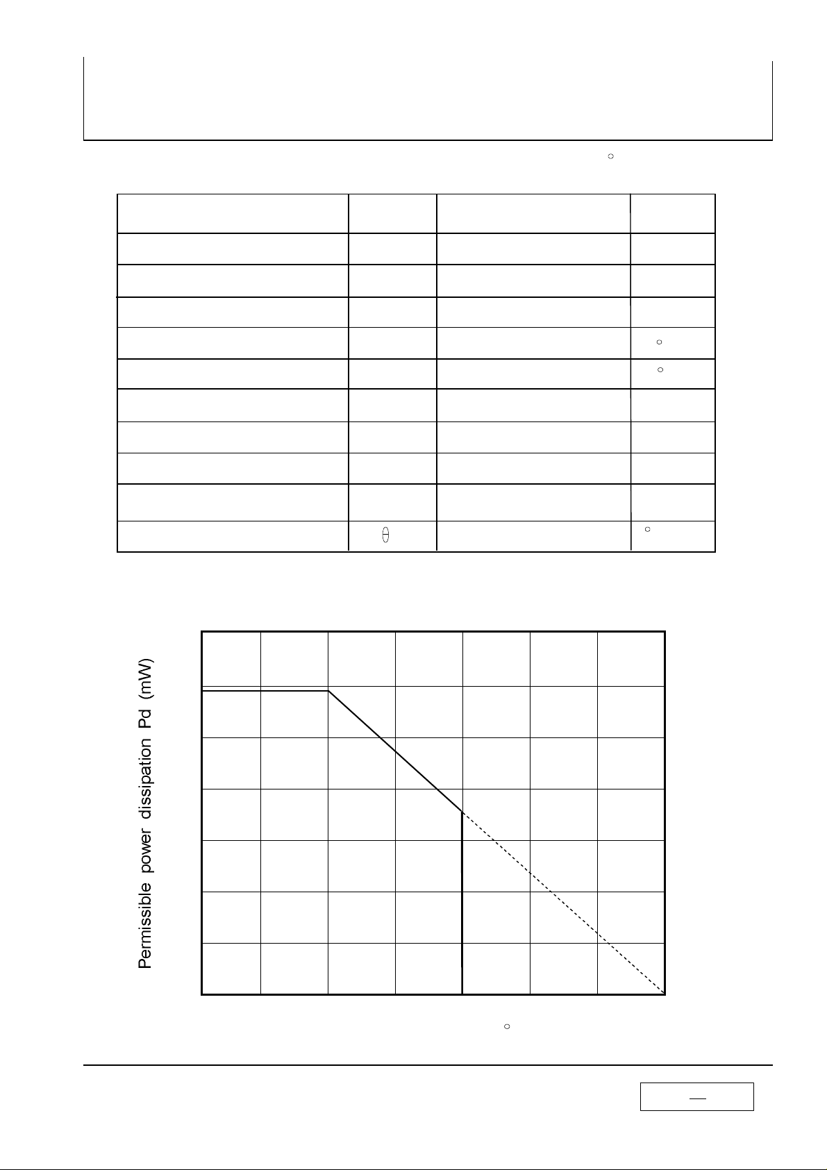
Thermal Derating Curve
2800
Vcc12
Vcc 5
Pd
Topr
Tstg
Vopr 12
Vopr 5
Vopr' 12
Vopr' 5
jc
13.0
6.0 V
2358
-20~ +75
-40~ +150
12.0
5.0
10.5~12.5 ( Typ 12.0V )
4.5~5.5 ( Typ 5.0V )
28
V
mW
C
C
V
V
V
V
C/W
2400
2358
2000
1600
1200
800
400
-20
1415
attached
board
0
25 50
75
100 125 150
Ambient temperature Ta( C)
MITSUBISHI
2
25
Page 3
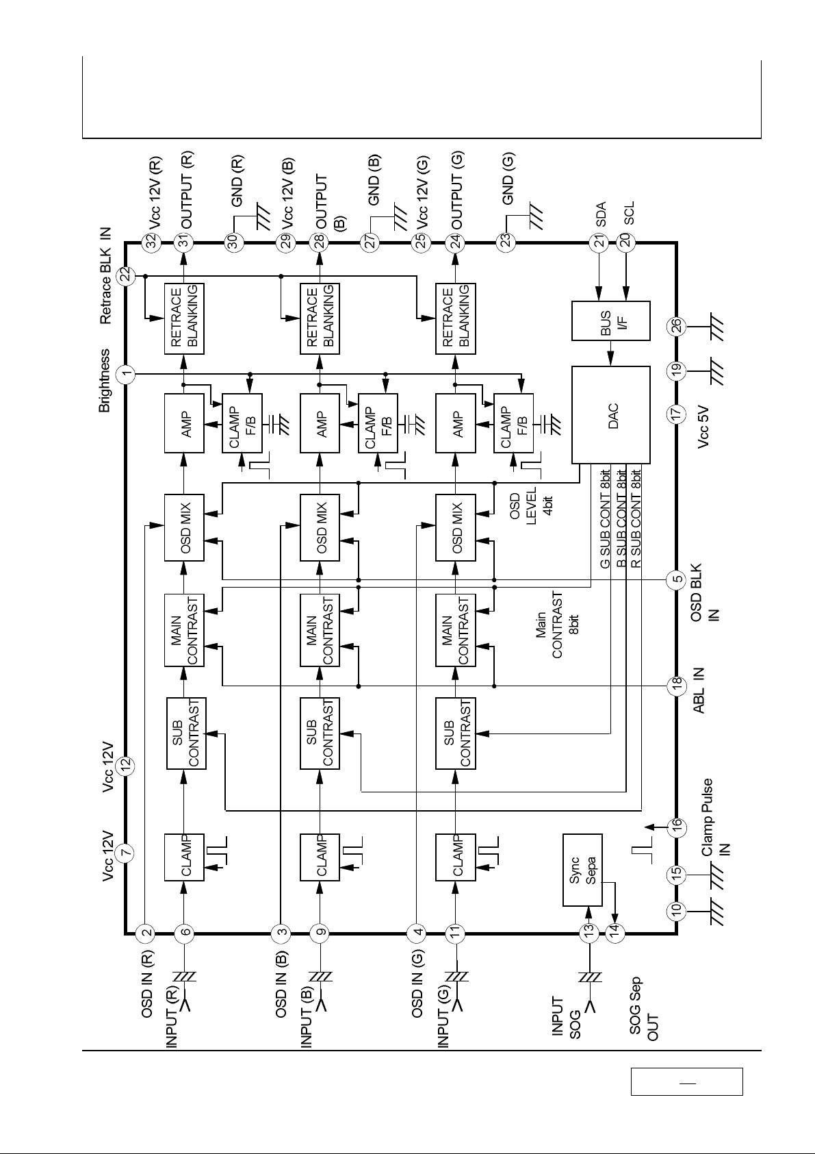
Fig. 1
Block Diagram
MITSUBISHI< LINEAR IC >
M52746SP
BUS CONTROLLED 3CH VIDEO PRE-AMP FOR CRT DISPLAY MONITOR
MITSUBISHI
3
25
Page 4
BUS CONTROL TABLE
(1) Slave address:
D7 D6 D5 D4 D3 D2 D1 R/W
0
1
0
(2) Each function's sub address:
0 1 0
MITSUBISHI< LINEAR IC >
M52746SP
BUS CONTROLLED 3CH VIDEO PRE-AMP FOR CRT DISPLAY MONITOR
0 0
=88H
NO.
1
2
3
4
5
function bit sub
add. D7 D6 D5 D4 D3 D2 D1 D0
Main contrast 8
Sub contrast R 8
Sub contrast G 8
Sub contrast B 8
OSD level 4 - - - - A43 A42 A41 A40
00H
01H
02H
03H
04H
Data Byte(up:bit information down:preset)
A07 A06 A05 A04 A03 A02 A01 A00
0 1 0 0 0 0 0 0
A17 A16 A15 A14 A13 A12 A11 A10
1 0 0 0 0 0 0 0
A27 A26 A25 A24 A23 A22 A21 A20
1 0 0 0 0 0 0 0
A37 A36 A35 A34 A33 A32 A31 A30
1 0 0 0 0 0 0 0
0 0 0 0 1 0 0 0
MITSUBISHI
4
25
Page 5
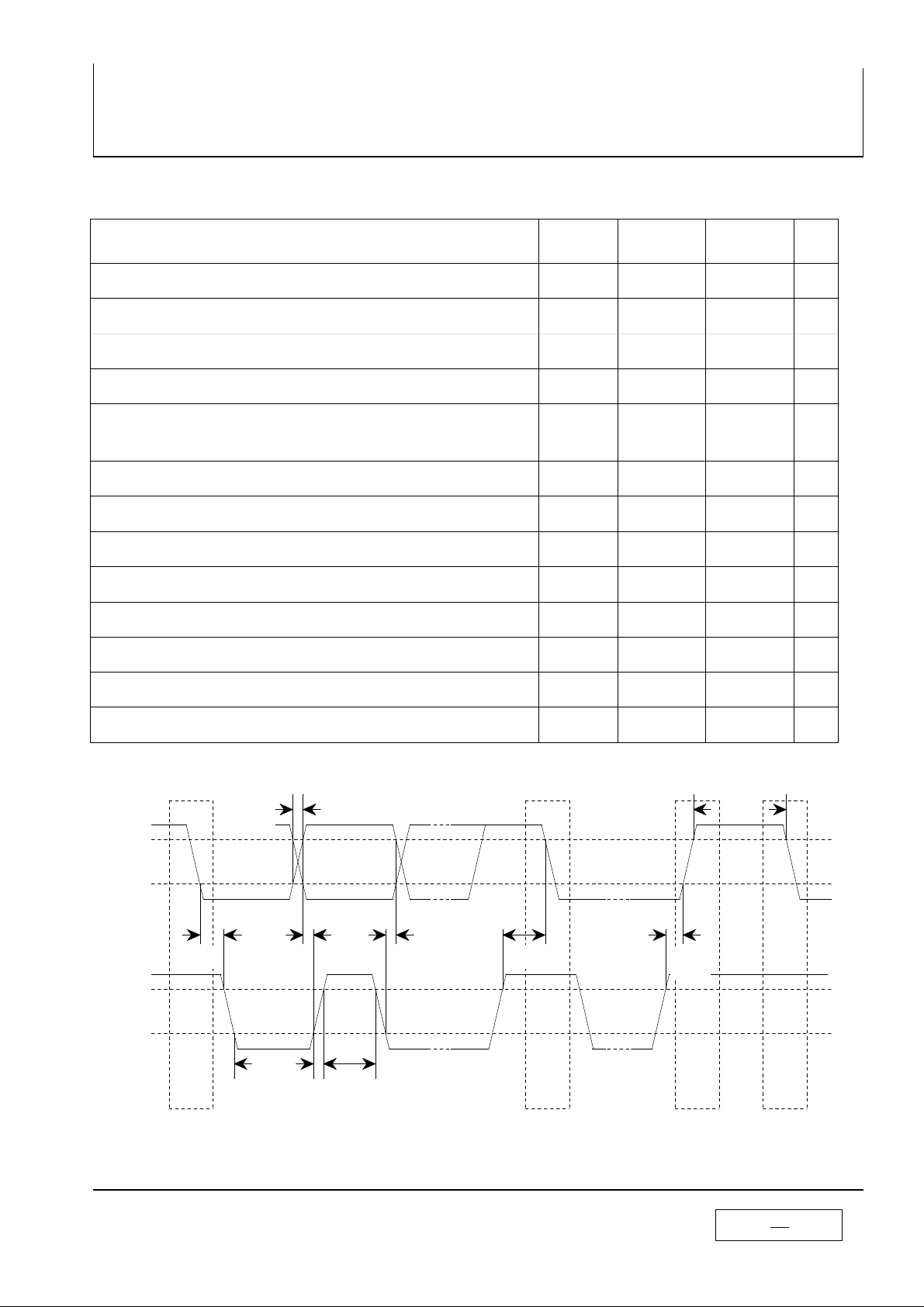
I C BUS CONTROL SECTION
2
SDA,SCL CHARACTERISTICS
MITSUBISHI< LINEAR IC >
M52746SP
BUS CONTROLLED 3CH VIDEO PRE-AMP FOR CRT DISPLAY MONITOR
parameter
min. input LOW voltage.
max. input HIGH voltage.
SCL clock frequency.
Time the bus must be free before a new transmission can start.
Hold time start condition.After this period the first clock pulse
is generated.
The LOW period of the clock.
The HIGH period of the clock.
Srt up time for start condition. (Only relevant for a repeated
start condition.)
Hold time DATA.
Set-up time DATA.
Rise time of both SDA and SCL lines.
symbol
VIL
VIH
fSCL
tBUF
tHD:STA
tLOW
tHIGH
tSU:STA
tHD:DAT
tSU:DAT
tR
MIN MAX
-0.5 1.5
3.0
0 100 KHz
4.7
4.0
4.7
4.0
4.7
0
250
-
5.5 V
-
-
-
-
-
-
-
1000
unit
V
us
us
us
us
us
us
ns
ns
Fall time of both SDA and SCL lines.
Set-up time for stop condition.
tR, tF
VIL
SDA
VIH
tHD:STA
tSU:DAT
VIL
SCL
VIH
tLOW
S S P S
tHIGH
tHD:DAT
tSU:STA
tF
tSU:STO
4.0
-
tSU:ST
O
300
tBUF
ns
-
us
MITSUBISHI
5
25
Page 6
MAX
22
00H
cont
01H
02H
03H
04H
R
G
B
Adj
Re-
Circuit current1
Variable
255
255
255
255
0
100
255
200
100
20
255
100
100
100
200
200
200
17.1
17.7
16.5
10.5
16.5
12.0
255
Circuit current2
range
Maximum input
Maximum gain
maximum gain
characteristics 1
characteristics 1
characteristics 1
characteristics 1
characteristics 2
characteristics 2
characteristics 3
characteristics3
characteristics 2
characteristics 2
Note1
Note2
Note3
Note4
Note5
Note6
Note7
Note8
Note9
Note10
Note11
Note13
Note15
Note12
Note14
Note16
mark
Unit
Standard
MIN TYP
OSD
BUS CTL ( H )
Sub
cont
Sub
cont
Sub
cont
Main
18
ABL
1
CTL voltage
Bright
mA
00H
FFH
FFH
FFH
FFH
5.0
4.0
135
110
-
mA
35
18
-
5.0
4.0
Vp-p
-
6.0 8.0
5.0
Variable
64H
Vp-p
-
-
1.6
5.0
2.0
dB
FFH
19.4
5.0
2.0
-
0.8 1.0 1.2
-
-
-
dB
C8H
19.0
15.0
5.0
2.0
-
0.8 1.0 1.2
-
-
-
64H
dB
13.0
9.0
5.0
2.0
-
0.8 1.0 1.2
-
-
-
14H
Vp-p
0.1 0.5 0.8
5.0
2.0
-
-
-
-
0.8 1.0 1.2
C8H
C8H
C8H
FFH
dB
19.0
15.5
5.0
2.0
-
0.8 1.0 1.2
-
-
-
-
-
-
64H
64H
64H
FFH
dB
13.0
9.0
2.0 5.0
-
0.8 1.0 1.2
-
-
-
-
-
-
In
13
SOG
a a
16
ReT
CP In
BLK
b
SG5
a a
b
Input
2 3 4
OSD In
a a
a
IA
Icc1
a a
a
IB
Icc2
5
OSD
7 9 11
Test
Point(s)
Symbol
BLK
RGB In
parameter
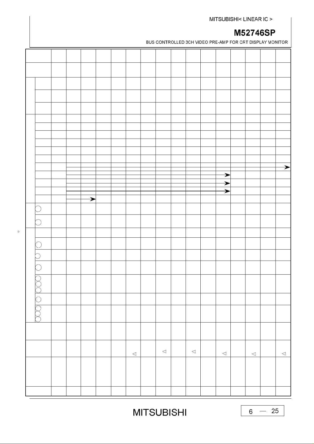
Supplementary Table1 Electrical Characteristics (Vcc= 12V,5V; Ta= 25 C unless otherwise specified)
No
1
2
a a
a a
a a
SG5bSG5bSG5bSG5
a
a
a a
a a
b
b
SG2
OUT
Vomax
Output dynamic
3
SG2
IN
OUT
Vimax
4
B
SG1
OUT
Gv
5
-
-
-
-
-
-
-
Gv
Relative
6
aa
b
SG5
aa
b
AG1
OUT
VC1
control
Main contrast
Main contrast
7
-
-
a a
-
b
SG5
-
-
a a
-
b
SG1
OUT
VC1
VC2
control
Main contrast
control relative
8
9
-
-
-
b
-
-
-
b
-
VC2
Main contrast
Main contrast
control relative
10
SG5
a a a a
SG1
OUT
VC3
control
11
-
-
-
b
-
-
-
b
-
VC3
Sub contrast
Main contrast
control relative
12
SG5
a a a a
SG1
OUT
VSC1
control
13
-
-
-
-
-
-
-
VSC1
Sub contrast
Sub contrast
control relative
14
b
a a a a
b
OUT
VSC2
control
15
SG5
SG1
Sub contrast
-
-
-
-
-
-
-
VSC2
control relative
16
Page 7
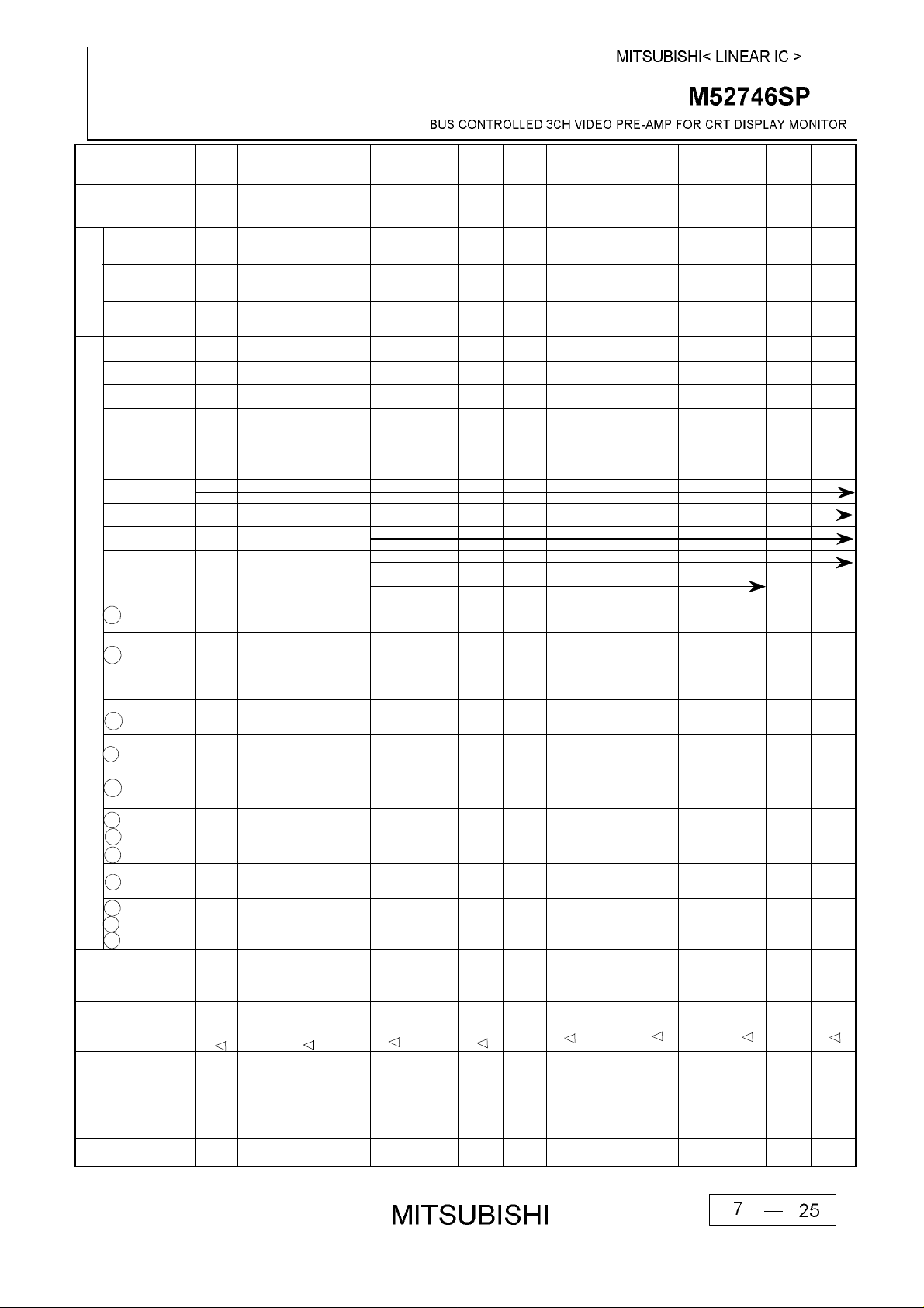
MAX
22
00H
cont
01H
02H
03H
04H
R
G
B
Adj
Re-
characteristics 1
ABL1
ABL1
255
20
20
20
0
200
200
200
200
255
255
255
255
Note17
Note18
Note19
Note20
Note21
Note22
Note23
Note24
Note25
Note26
Note27
Note29
Note31
Note28
Note30
Note32
characteristics 3
characteristics 3
characteristics
characteristics 1
characteristics2
characteristics 2
characteristics 1
characteristics 1
characteristics 2
characteristics 2
characteristics 3
characteristics 3
(f=50MHz)
(f=50MHz)
able
mark
Unit
Standard
MIN TYP
OSD
BUS CTL ( H )
Sub
cont
Sub
cont
Sub
cont
Main
18
ABL
1
CTL voltage
Bright
00H
14H
14H
14H
FFH
0.1 0.5 0.8 Vp-p
2.0 5.0
-
0.8 1.0 1.2
-
-
-
-
-
C8H
C8H
C8H
C8H
Vp-p
4.63.6 4.8
2.0 5.0OUT
-
-
-
-
-
-
-
0.8 1.0 1.2
FFH
FFH
FFH
FFH
Vp-p
4.7 5.5 6.3
2.0 4.0OUT
-
0.8 1.0 1.2
-
-
Vp-p
1.7 2.2 2.7
2.0
2.0
-
0.8 1.0 1.2
-
-
V
3.3 3.8 4.2
4.0 5.0OUT
-
-0.3 0 0.3
-
-
V
1.5 1.8 2.1
2.0 5.0OUT
-
-0.3 0 0.3
-
-
V
0.5 0.9 1.1
1.0 5.0OUT
-
-0.3 0 0.3
-
-
Vari
dB
2.5
0
-2.0
5.0OUT
-1.0 0 1.0 dB
-
-
-
13
16
Input
7 9 11
Test
In
SOG
ReT
BLK
CP In
2 3 4
OSD In
5
OSD
BLK
RGB In
Point(s)
Symbol
Sub contrast
parameter
No
a
a
b
a a
b
OUT
VSC3
control
17
SG5
SG1
Sub contrast
-
-
a a
- -
b
SG5
- -
a a
b
SG1
- -
VSC3
VMSC
Main/sub
control relative
contrast control
18
19
a a
b
SG5
- -- - - --
a a
b
SG1
VMSC
ABL control
control relative
characteristics
Main/sub contrast
20
21
- -- - - --
relative
ABL control
22
a a
b
SG5
a a
b
SG1
OUT
ABL2
ABL control
ABL control
23
- -- - - --
ABL2
relative
24
a
a
b
SG5
a a
a
VB1
control
Brightness
25
- -- - - --
VB1
Brightness
Brightness
control relative
26
a a
b
a a
a
VB2
control
27
SG5
Brightness
a a
b
SG5
a a
- -- - - --
a
VB2
VB3
control
Brightness
control relative
28
29
- -- - - --
VB3
Brightness
control relative
30
a
a
a
5V
a a
b
SG3
FC1
Frequency
characteristics 1
Frequency relative
31
- -- - - --
FC1
characteristics 1
32
Page 8
MAX
22
00H
cont
01H
02H
03H
04H
R
G
B
Adj
Re-
0
255
255
255
OUT(32)
11a
11a
11b SG3
11a
OUT(35)
11a
OUT(35)
11b SG3
Variable
255
255
Variable
OUT(32)
OUT(35)
OUT(35)
1 (f=200MHz)
2 (f=200MHz)
voltage
characteristics 1
characteristics 2
Note33
Note34
Note35
Note36
Note37
Note38
Note39
Note40
Note41
Note42
Note43
Note44
Note45
Note46
Note47
Note48
Variable
ble
ble
ble
mark
Unit
Standard
MIN TYP
OSD
BUS CTL ( H )
Sub
cont
Sub
cont
Sub
cont
Main
00H
FFH
FFH
FFH
-3.0 0 3.0 dB
-1.0 0 1.0 dB
-3.0 3.0 5.0 dB
-1.0 0 1.0 dB
FFH
-25 -20 dB
-
-20 -15 dB
-
-25 -20 dB
-
-20 -15 dB
-
-25 -20 dB
-
-20 -15 dB
-
nS
2.8
2.2
-
nS
2.8
2.2
-
FFH
V
V
-
1.0 1.5 2.0 V
0.2 - uS
-3.0 0 0.3
-3.0 0 0.3
18
1
13
Bright
SOG
CTL voltage
ReT
16
Input
2 3 4
5
OSD
7 9 11
Test
Point(s)
Symbol
ABL
a
In
a
BLK
a
CP In
OSD In
a a
BLK
b
RGB In
5.0
5V
SG3
OUT
FC1'
--
-
- - --
FC1'
5.0OUT
Variable
a a
a
a a
b
FC2
5V
SG3
- - -- - --
FC2
5.0
Variablea a
a a
a
5V
2 b SG3
6 a
OUT(29)
CT1
5.0
Variable
a
5V
a a a a
2 b SG3
6 a
OUT(29)
CT1'
5.0
Variablea a a a
a
2 a
6 b SG3
OUT(29)
CT2
5V
5.0
Variablea a a a
a
2 a
6 b SG3
OUT(29)
CT2'
5V
5.0
Variablea a a a
a
2 a
6 a
OUT(32)
CT3
5V
5.0
Variablea a a a
a
5V
2 a
6 a
OUT(32)
CT3'
5.0OUT
5.0OUT
2.0 5.0OUT
2.0 5.0OUT
2.0 5.0OUT
Variablea a a a
Variablea a a a
a
a
a
a
SG5
b
b
a
5V
b
a
5V
SG5
a
a a
a
b
b
b
SG1
VthCP
b
SG1bSG1
WCP
Tr
SG1
SG1
Tf
2.0 5.0OUT
a
a
a
a
SG5bSG5
a
a a
a
b
PDCL
PDCH
SG1
Frequency
parameter
No
Frequency relative
33
characteristics 1
34
characteristics
(f=200MHz)
Frequency
characteristics
characteristics 2
Frequency relative
35
(f200MHz)
Crosstalk 1
36
(f=50MHz)
Crosstalk 1
37
Crosstalk 2
(f=200MHz)
38
39
(f=50MHz)
Crosstalk 2
(f=200MHz)
40
(f=50MHz)
Crosstalk 3
Crosstalk 3
41
Pulse
(f=200MHz)
characteristics 1
42
43
Pulse
(4Vp-p)
characteristics 2
44
(4Vp-p)
Clamp pulse
threshold
45
Clamp pulse
temperature
Pedestal voltage
minimum width
46
Pedestal voltage
47
temperature
48
Page 9

MAX
22
00H
cont
01H
02H
03H
04H
R
G
B
Adj
Re-
VthOSD1
8
255
255
255
255
Sync OUT
15
8
0
8
0
Variable
Variable
Variable
8
characteristics 1
characteristics 2
characteristics 2
voltage 1
Variable
voltage
voltage
Note49
Note50
Note51
Note52
Note53
Note54
Note55
Note56
Note57
Note58
Note59
Note60
Note61
Note62
Note63
Note64
Variable
VthOSD2
8
Variable
voltage 2
15
3V
0
3V
8
characteristics 2
mark
Unit
Standard
MIN TYP
OSD
BUS CTL ( H )
Sub
cont
Sub
cont
Sub
cont
Main
18
ABL
1
CTL voltage
Bright
08H
FFH
FFH
FFH
FFH
ns
3.0 6.0
-
2.0 5.0
08H
3.0 6.0 ns
-
2.0 5.0OUT
0FH
7.2 Vp-p
6.4
5.6
2.0 5.0
-
0.8 1.0 1.2
-
- -
08H
3.4 4.0 4.6 Vp-p
2.0 5.0OUT a a
-
0.8 1.0 1.2
-
- -
00H
Vp-p
1.2
0.7
0
2.0 5.0
-
0.8 1.0 1.2
-
08H
3.1 3.5 3.9 V
2.0 5.0OUT
08H
1.5 2.0 2.5 Vaa
2.0 5.0OUT
2.2 2.7 3.2 Va
00H
2.0 5.0
0FH
3.7 4.3 4.9 Vp-p
2.0 5.0
08H
00H
1.0 1.5 2.0 V
2.0 5.0
Vp-p
0.03
-
-
2.0 5.0
Vp-p-
-
0.2
2.0 5.0
13
16
Input
7 9 11
Test
In
SOG
ReT
BLK
CP In
2 3 4
OSD In
5
OSD
BLK
RGB In
Point(s)
Symbol
parameter
OSD pulse
No
a a
a a
b
SG5bSG5bSG5
b
SG6bSG6bSG6
a
a
a
a
OUT
OTf
OTr
OSD pulse
OSD adjust
49
50
a
- -
a
-
b
control
- -
SG6
-
a
-
OUT
Oaj1
Oaj1
OSD adjust
control relative
characteristics 1
51
52
b
SG5
b
SG6
b
SG6
a
Oaj2
control
OSD adjust
OSD adjust
characteristics 1
characteristics 2
53
a
a
- -
b
-
b
b
- -
a
-
-
OUT
Oaj2
Oaj3
control
OSD adjust
control relative
54
55
SG5
SG6
SG6
b
- -- - - -- - -
Oaj3
OSD input
OSD adjust
control relative
characteristics 3
characteristics 3
56
aa
b
SG5
SG6
b
SG6
a
threshold
57
b
SG5
b
SG6
b
SG6
a
threshold
OSD input
58
a
b
b
SG5
a
b
SG6
b
b
SG6
SG1
b
OUT
control
threshold
OSD BLK input
OSD half adjust
59
a
a
b
SG5
SG5
b
SG6
b
SG6
SG6
a 1.9 2.5 3.0 Vp-p
a
OUT
Ohaj2 2.0 5.0OUT a a
Ohaj1
control
OSD half adjust
characteristics 1
60
61
a
b
b
SG7
b
SG5
a
a
a
OUT
VthRET
voltag
SOG input
Retrace BLK i
nput threshold
62
b
SG4
SG4
a
a
a
a
a
a a
a
a
a
S on G IN
S on G IN
Sync OUT
SS - SV
maximum noize
63
input voltage
SOG minimum
64
Page 10

MAX
22
00H
cont
01H
02H
03H
04H
R
G
B
Adj
Re-
VSL
Ips
255
255
255
255
0
10.0
10.4
1
5
mode)
Note65
Note66
Note67
Note68
Note69
Note70
5
255
255
255
255
0
Unit
mark
mA
VDC
Standard
MIN TYP
OSD
BUS CTL ( H )
Sub
cont
Sub
cont
Sub
cont
Main
18
ABL
1
13
Bright
SOG
CTL voltage
ReT
16
In
BLK
CP In
0 0.3 0.6 V
2.0 5.0
a
a
SG4
0 60 90 ns
2.0 5.0
b
SG4bSG4
a
a
4.5 4.9 5.0 V
2.0 5.0
b
b
SG4
a
a
0 60 90 ns
2.0 5.0
a
a
b
00H
FFH
FFH
FFH
FFH
SG
- 22 30
4.0 5.0
a
a
9.4
00H
FFH
FFH
FFH
FFH
2.0 5.0
a
a
b
SG
Input
7 9 11
Test
2 3 4
OSD In
5
OSD
BLK
RGB In
Point(s)
Symbol
parameter
Sync Output Hi
No
a
a
a
Sync
VSH
Level
65
OUT
a
a
a
Sync
Level
66
OUT
Sync
Sync Output
a
a
a
a
a
a
OUT
Sync
TDS-F
TDS-R
Delay Time1
Sync Output
67
68
a
a
a
OUT
Iccps
Icc
(power save
Delay Time2
69
a
a
b
SG
Vcc
(12V)
skv
spot killer
70
Page 11

MITSUBISHI< LINEAR IC >
M52746SP
BUS CONTROLLED 3CH VIDEO PRE-AMP FOR CRT DISPLAY MONITOR
Note1) Measuring conditions are as listed in supplementary Table. Measured with a current
meter at test point IA.
Note2) Measuring conditions are as listed in supplementary Table. Measured with a current
meter at test point IB.
Note3) Decrease V1 gradually, and measure the voltage when the bottom of waveform output is
distorted. The voltage is called VCL.
Next, increase V1 gradually, and measure the voltage when the top of waveform output is
distorted. The voltage is called VOH.
Voltagr Vomax is calculated by the equation below:
Vomax = VOH - VOL
(V)
VOH
5.0
Waveform output
VOL
0.0
Note4) Increase the input signal(SG2) amplitude gradually, starting from 700mVp-p. Measure the
amplitude of the input signal when the output signal starts becoming distorted.
Note5) Input SG1, and read the amplitude output at OUT(24,28,31). The amplitude is called
VOUT(24,28,31).Maximum gain GV is calculated by the equation below:
VOUT
GV=20 LOG (dB)
Note6) Relative maximum gain GV is calculated by the equation below:
GV=VOUT(24)/VOUT(18), VOUT(28)/VOUT(31), VOUT(31)/VOUT(24)
Note7) Measuring the amplitude output at OUT(24,28,31). The measured value is called
VOUT(24,28,31).
Main contrast conrol characteristics VC1 is calculated by the equation below:
VC1=20 LOG
0.7
VOUT
(dB)
0.7
Note8) Relative characteristics VC1 is calculated by the equation below:
VC1=VOUT(24)/VOUT(28) , VOUT(28)/VOUT(31) , VOUT(31)/VOUT(24)
Note9) Measuring condition and procedure are the same as described in Note7.
Note10) Measuring condition and procedure are the same as described in Note8.
Note11) Measuring condition and procedure are the same as described in Note7.
Note12) Measuring condition and procedure are the same as described in Note8.
11
MITSUBISHI
25
Page 12

MITSUBISHI< LINEAR IC >
M52746SP
BUS CONTROLLED 3CH VIDEO PRE-AMP FOR CRT DISPLAY MONITOR
Note13) Measure the amplitude output at OUT(24,28,31). The measured value is called
VOUT(24,28,31).
Sub contrast conrol characteristics VSC1 is calculated by the equation below:
VSC1=20 LOG (dB)
Note14) Relative characteristics VSC1 is calculated by the equation below:
VSC1=VOUT(24)/VOUT(28) , VOUT(28)/VOUT(31) , VOUT(31)/VOUT(24)
Note15) Measuring condition and procedure are the same as described in Note13.
Note16) Measuring condition and procedure are the same as described in Note14.
Note17) Measuring condition and procedure are the same as described in Note13.
Note18) Measuring condition and procedure are the same as described in Note14.
Note19) Measure the amplitude output at OUT(24,28,31). The measured value is called
VOUT(24,28,31).
Main/Sub contrast conrol characteristics VMSC1 is calculated by the equation below:
VMSC1=20 LOG (dB)
VOUT
0.7
VOUT
0.7
Note20) Relative characteristics VMSC1 is calculated by the equation below:
VMSC=VOUT(24)/VOUT(28) , VOUT(28)/VOUT(31) , VOUT(31)/VOUT(24)
Note21) Measure the amplitude output at OUT(24,28,31). The measured value is called
VOUT(24,28,31), and is ttreated as ABL1.
Note22) Relative characteristics ABL1 is calculated by the equation below:
ABL1=VOUT(24)/VOUT(28) , VOUT(28)/VOUT(31) , VOUT(31)/VOUT(24)
Note23) Measuring condition and procedure are the same as described in Note21.
Note24) Measuring condition and procedure are the same as described in Note22.
Note25) Measure the DC voltage at OUT(24,28,31) with a voltmeter. The measured value is called
VOUT(24,28,31), and is ttreated as VB1.
Note26) Relative characteristics VB1 is calculated by the difference in the output between the
channels.
VB1=VOUT(24)-VOUT(28) , VOUT(28)-VOUT(31) , VOUT(31)-VOUT(24)
Note27) Measuring condition and procedure are the same as described in Note25.
Note28) Measuring condition and procedure are the same as described in Note26.
Note29) Measuring condition and procedure are the same as described in Note25.
Note30) Measuring condition and procedure are the same as described in Note26.
MITSUBISHI
12
25
Page 13

MITSUBISHI< LINEAR IC >
Note31) First, SG3 to 1MHz is as input signal. Input a resister that is about 2K to offer the voltage at input
M52746SP
BUS CONTROLLED 3CH VIDEO PRE-AMP FOR CRT DISPLAY MONITOR
pins(6,9,11) in order that the bottom of input signal is 2.5V.
Control the main contrast in order that the amplitude of sine wave output is 4.0Vp-p.
Control the brightness in order that the bottom of sine wave output is 2.0Vp-p.
By the same way, measure the output amplitude when SG3 to 50MHz is as input signal.
The measured value is called VOUT(24,28,31).
Frequency characteristics FC1(24,28,31) is calculated by the equation below:
FC1=20 LOG
output amplitude when inputed SG3(1MHz) : 4.0Vp-p
VOUT Vp-p
Note32) Relative characteristics FC1 is calculated by the difference in the output between the channels.
Note33) Measuring condition and procedure are the same as described in Note31,expect SG3 to 200MHz.
Note34) Relative characteristics FC1' is calculated by the difference in the output between the channels.
Note35) SG3 to 1MHz is as input signal. Control the main contrast in order that the amplitude of sine wave
output is 1.0Vp-p.
By the same way, measure the output amplitude when SG3 to200MHz is as input signal.
The measured value is called VOUT(24,28,31).
Frequency characteristics FC2(24,28,31) is calculated by the equation below:
FC2=20 LOG
output amplitude when inputed SG3(1MHz) : 4.0Vp-p
VOUT Vp-p
(dB)
(dB)
Note36) Relative characteristics FC2 is calculated by the difference in the output between the channels.
Note37) Input SG3 (50MHz) to pin2 only, and then measure the waveform amplitude output at
OUT(24,28,31).The measured value is called VOUT(24,28,31).
Crosstalk CT1 is calculated by the equation below:
CT1=20 LOG
VOUT(24,28)
VOUT(31)
(dB)
Note38) Measuring condition and procedure are the same as described in Note37,expect SG3 to 200MHz.
Note39) Input SG3 (50MHz) to pin6 only, and then measure the waveform amplitude output at
OUT(24,28,31).The measured value is called VOUT(24,28,31).
Crosstalk CT2 is calculated by the equation below:
CT2=20 LOG
VOUT(24,31)
VOUT(28)
(dB)
Note40) Measuring condition and procedure are the same as described in Note39,expect SG3 to 200MHz.
Note41) Input SG3 (50MHz) to pin11 only, and then measure the waveform amplitude output at
OUT(24,28,31).The measured value is called VOUT(24,28,31).
Crosstalk CT2 is calculated by the equation below:
CT3=20 LOG
VOUT(28,31)
VOUT(24)
(dB)
Note42) Measuring condition and procedure are the same as described in Note41,expect SG3 to 200MHz.
13
25
MITSUBISHI
Page 14

MITSUBISHI< LINEAR IC >
pulse to rise from 10 % to 90 % (Tr2) with an active prove.
M52746SP
BUS CONTROLLED 3CH VIDEO PRE-AMP FOR CRT DISPLAY MONITOR
Note43) Control the main contrast (00H) in order that the amplitude of output signal is 4.0Vp-p.
Control the brightness (V1) in order that the Black level of output signal is 2.0V.
Measure the time needed for the input pulse to rise from 10 % to 90 % (Tr1) and for the
output
Pulse characteristics Tr is calculated by the equations below :
Tr = (Tr2) - (Tr1) (nsec)
2 2
Note44) Measure the time needed for the input pulseto fall from 90 % to 10 % (Tf1) and for the
output
pulse to fall from 90 % to 10 % (Tf2) with an active prove.
Pulse characteristics Tf is calculated by the equations below :
Tf = (Tf2) - (Tf1) (nsec)
100%
0%
2 2
Tr1
or
Tr2
90%
10%
Tf1
or
Tf2
Note45) Turn down the SG5 input level gradually from 5.0Vp-p, monitoring the waveform output.
Measure the top level of input pulse when the output pedestal voltage turn decrease with
unstable.
Note46) Decrease the SG5 pulse width gradually from 0.5us, monitoring the output. Measure the
SG5 pulse width (a point of 1.5V) when the output pedestal voltage turn decrease with
unstable.
Note47) Measure the pedestal voltage at 25 C. The measured value is called PDC1.
Measure the pedestal voltage at temperature of -20 C. The measured value is called
PDC2.
Pedestal voltage temperature characteristics 1 is calculated by the equation below:
PDCH=PDC1-PDC2
Note48) Measure the pedestal voltage at 25 C. The measured value is called PDC1.
Measure the pedestal voltage at temperature of 75 C. The measured value is called PDC3.
Pedestal voltage temperature characteristics 2 is calculated by the equation below:
PDCL=PDC1-PDC3
14
25
MITSUBISHI
Page 15

MITSUBISHI< LINEAR IC >
Measure the SG6 level when the output reaches 0V. The measured value is called VthOSD2.
M52746SP
BUS CONTROLLED 3CH VIDEO PRE-AMP FOR CRT DISPLAY MONITOR
Note49) Measure the time needed for the output pulse to rise from 10% to 90%(OTR) with an active prove.
Note50) Measure the time needed for the output pulse to fall from 90% to 10% (OTF) with an active prove.
Note51) Measure the amplitude output at OUT(24,28,31). The measured value is called VOUT(24,28,31),
and is treated as Oaj1.
Note52) Relative characteristics Oaj1 is calculated by the equation below:
Oaj1=VOUT(24)/VOUT(28), VOUT(28)/VOUT(31), VOUT(31)/VOUT(24)
Note53) Measuring condition and procedure are the same as described in Note51.
Note54) Measuring condition and procedure are the same as described in Note52.
Note55) Measuring condition and procedure are the same as described in Note51.
Note56) Measuring condition and procedure are the same as described in Note52.
Note57) Reduce the SG6 input level gradually, monitoring output.
Measure the SG6 level when the output reaches 65~75% of first voltage. The measured value is
called VthOSD1.
Note58) Reduce the SG6 input level gradually, monitoring output.
Note59) Confirm that output signal is being blanked by the SG6 at the time.
Monitoring to output signal, decreasing the level of SG6. Measure the top level of SG6 when the
blanking period is disappeared. The measured value is called VthBLK.
Note60) Measure the amplitude output at OUT(24,28,31). The measured value is called VOUT(24,28,31),
and is treated as Ohaj1.
Note61) Measure the amplitude output at OUT(24,28,31). The measured value is called VOUT(24,28,31),
and is treated as Ohaj2.
Note62) Confirm that output signal is being blanked by the SG7 at the time.
Monitoring to output signal, decreasing the level of SG7. Measure the top level of SG7 when the
blanking period is disappeared. The measured value is called VthRET.
15
25
MITSUBISHI
Page 16

MITSUBISHI< LINEAR IC >
Note63) The sync's amplitude of SG4 be changed all white into all black, increase from 0Vp-p to 0.03Vp-p.
Measure the time needed for the rear edge of SG4 sink to fall from 50 % and for SyncOUT to rise
M52746SP
BUS CONTROLLED 3CH VIDEO PRE-AMP FOR CRT DISPLAY MONITOR
No pulse output permitted.
Note64) The sync's amplitude of SG4 be changed all white or all black, decrease from 0.3Vp-p to 0.2Vp-p.
Confirm no malfunction produced by noise.
Note65) Measure the high voltage at SyncOUT. The measured value is treated as VSH.
Note66) Measure the low voltage at SyncOUT. The measured value is treated as VSL.
Note67) SyncOUT becomes High with sink part of SG4.
from 50 % with an active prove. The measured value is treated as TDS-F ,less than 90nsec.
Note68) Measure the time needed for the rear edge of SG4 sink to rise from 50 % and for SyncOUT to fall
from 50 % with an active prove. The measured value is treated as TDS-R ,less than 90nsec.
SG4
sync (50%)
SyncOUT
Note69) No input at the Vcc of 12V when same condition by Note2 . Measure the AC current at Vcc(5V).
The measured value is treated as Iccps.
Note70) The Vcc of 12V be changed all white into all black, increase from 12V to 0V.
Measure the DC voltage at the Vcc When no output signal at R, G and Bout.
The measured value is treated as skv.
TDS-F
(50%)
TDS-R
Pedestal voltage
16
25
MITSUBISHI
Page 17

MITSUBISHI< LINEAR IC >
SG No.
INPUT SIGNAL
SG1
(all white)
SG2
(step wave)
SG3
SG4
SG5
pulse
SG6
OSD pulse
SG7
BLK pulse
M52746SP
BUS CONTROLLED 3CH VIDEO PRE-AMP FOR CRT DISPLAY MONITOR
Video signal
Video signal
Sine wave
(for freq. char.)
8us
33us
Pulse with amplirude of
0.7Vp-p (f=30KHz).
Video width of 25us. (75 % )
0.7VPP
0.7VP-P
(Amplitude is partially variable.)
Sine wave amplitude of 0.7Vp-p.
f=1MHz,50MHz,200MHz(variable)
Video width of 25us. (75 % )
0.7VP-P
all white or all black
variable.
Videosignal
(all white,all black)
Clamp
5us
3us
0.5us
5us
5VTTL
0.3VPP
Amplitude is partially
variable.
Amplitude is partially variable.
Sync's amplitude
is variable.
Pulse width and
amplitude are variable.
5VTTL
5VTTL
MITSUBISHI
*)f=30KHz
17
25
Page 18

TEST CIRCUIT
+
MITSUBISHI< LINEAR IC >
M52746SP
BUS CONTROLLED 3CH VIDEO PRE-AMP FOR CRT DISPLAY MONITOR
+
+
MITSUBISHI
18
25
Page 19

OSD IN (R)
OSD IN (B)
OSD IN (G)
Terminal Description
2.5
2.5V
INPUT (R)
INPUT (B)
INPUT (G)
Input at low impedance.
Input pulses
Main Brightness
1
OSD BLK IN
RGB
Input pulses
12
VCC
No.
1
Name
DC
Voltage
(V)
MITSUBISHI< LINEAR IC >
M52746SP
BUS CONTROLLED 3CH VIDEO PRE-AMP FOR CRT DISPLAY MONITOR
peripheral Circuit
35K
It is recommended that the
IC be used between pedestal
voltage 2V and 3V.
Remark
2
1K
3
2.0V
2K
3.5V
2.7V
2K
4
5
0.5mA
5
0.4mA
Connected to GND if
not used.
Connected to GND if
not used.
Clamped to about 2.5 V
due to clamp pulses
from pin 19.
4.0~5V(light)
2.5~3V(half)
1.5V~GND
3.7~5V
1.7V~GND
6
9
11
7
12
CP
0.3mA
MITSUBISHI
Vcc
19
25
Page 20

MITSUBISHI< LINEAR IC >
NC
18
INPUT (S on G)
7
GND
GND
16
Clamp Pulse IN
Input pulses
Input at low impedance.
17
VCC (5V)
M52746SP
BUS CONTROLLED 3CH VIDEO PRE-AMP FOR CRT DISPLAY MONITOR
No.
8
10
15
19
26
13
Name
DC
Voltage
(V)
When
open
~
2.5V
~
peripheral Circuit
1K
3.2V
500
Remark
SYNC ON VIDEO input pin.
Sync is negative.
input signal at Pin7, compare
with the reference voltage
of internal circuit in order to
separate sync signal from
Sync on Green signal.
Sync signal output pin,
Being of open collector output
type.
14
S on G Sep OUT
41K
2.5~5V
0.5V
19
2.2V
0.15mA
maximum
MITSUBISHI
20
25
Page 21

20
20
SCL
21
21
SDA
2
2
No.
ABL IN
15
18
22
2.25V
R
G
B
Input pulses
0.5V
Name
DC
Voltage
(V)
When
open
2.5V
0.5mA
MITSUBISHI< LINEAR IC >
M52746SP
BUS CONTROLLED 3CH VIDEO PRE-AMP FOR CRT DISPLAY MONITOR
peripheral Circuit
20K
1.2K1.2K 30K
50K
2.5V
ABL(Automatic Beam Limitter)
input pin.
Recommended voltage range
is 0 to 5V.
When ABL function is not used,
set to 5V.
SCL of I C BUS
(Serial clock line)
VTH=2.3V
Remark
Retrace BLK IN
2K
3V
SDA of I C BUS
50K
2K
3V
50K
22
(Serial data line)
VTH=2.3V
2.5~5V
maximum
Connected to GND if not
used.
MITSUBISHI
21
25
Page 22

No.
2550VCC 2
12
ssed
28
OUTPUT (G)
31
OUTPUT (R)
24
OUTPUT (B)
27
GND (G)
30
GND (R)
23
GND (B)
0
29
32
Name
DC
Voltage
(V)
MITSUBISHI< LINEAR IC >
M52746SP
BUS CONTROLLED 3CH VIDEO PRE-AMP FOR CRT DISPLAY MONITOR
peripheral Circuit
GND of Rch, Gch and Bch
Remark
Variable
Impre
-
50
A resistor is needed on the GND
side.
Set discretionally to maximum
15 mA, depending on the required
driving capacity.
Used to supply power to
output emitter follower only.
MITSUBISHI
22
25
Page 23

MITSUBISHI< LINEAR IC >
Electrical Chracteristics
M52746SP
BUS CONTROLLED 3CH VIDEO PRE-AMP FOR CRT DISPLAY MONITOR
Main Contrast Control Characteristics
6
4
2
Sub Contrast : MAX
0
00H
Main Contrast Control Data
OSD Adjust Control Characteristics
6
FFH
Sub Contrast Control Characteristics
6
4
2
Main Contrast : MAX
0
00H
Sub Contrast Control Data
ABL Characteristics
FFH
4
2
0
0H
OSD Adjust Control Data
Brightness Control Characteristics
6
4
2
FH
1u
7
100K
12
Main Contrast : MAX
Sub Contrast : MAX
0
ABL Control Voltage(VDC)
Sync separate input min sync width
5
(Video Duty=75 % )
8
Sync separate
normal operating range
4
0
0
Brightness Control Voltage(VDC)
5
IN
0
MITSUBISHI
input amplitude(Vp-p)
23
0.5
25
Page 24

CLAMP PULSE INPUT
Application Method for M52746SP
Clamp pulse width is recommended
above 15 KHz, 1.0 usec
above 30 KHz, 0.5 usec
above 64 KHz, 0.3 usec .
MITSUBISHI< LINEAR IC >
M52746SP
BUS CONTROLLED 3CH VIDEO PRE-AMP FOR CRT DISPLAY MONITOR
19
The clamp pulse circuit in ordinary set is a long round
about way, and beside high voltage, sometimes
connected to external terminal, it is very easy affected
by large surge.
Therefore, the Fig. shown right is recommended.
Notice of application
Make the nearest distance between output pin and pull down resister.
Recommended pedestal voltage of IC output signal is 2V.
~
MITSUBISHI
24
25
Page 25

APPLICATION
EXAMPLE
110V
12345678910111213141516171832313029282726252423222120
19
M52746SP
3.3u
1K
0.01u
0.01u
3.3u
75
100K
0.01u
47u
0.01u
47u
0.01uu
3.3u
0.01u
75
47u
5V
5V
5V
5V
0~5V
Cut Off Adjj
1K1K1K
1u
75NC4.7u
0.01u
4.7u
0.01u
4.7u
0.01u
2.5V
2.5V
2.5V
MITSUBISHI< LINEAR IC >
M52746SP
BUS CONTROLLED 3CH VIDEO PRE-AMP FOR CRT DISPLAY MONITOR
CRT
DAC IC
TTL
BLK IN
(for retrace)
5VTTL
SDA
0 ~ 5V
SCL
ABL IN
Sync Sep
OUT
ClampPulse
TTL
TTL
TTL
TTL
TTL
TTL
IN
BLK IN
(for OSD)
OSD IN (G)
OSD IN (B)
OSD IN (R)
12V
5V
INPUT
(R)
INPUT
(B)
INPUT
(G)
MITSUBISHI
SONG
INPUT
25
25
 Loading...