

Page 1
MITSUBISHI ICs (Monitor)
M52733SP
3-CHANNEL VIDEO AMPLIFICATION WITH OSD BLANKING
DESCRIPTION
The M52733SP is a semiconductor integrated circuit amplifies
video signals, having a 3-channel amplifier with a band width of
130MHz. The circuit also features the OSD blanking function.
The circuit is most useful with high resolution displays that have
OSD, and its function are a vailable for each channel, including OSD
blanking, wide-band amplification, contrast control (main and sub),
and brightness control.
FEATURES
•
Frequency band width: RGB................................130MHz (3V
Input :RGB.............................................................0.7V
BLK ...............................................3.0V
P-P
min. (positive)
Output :RGB...........................................................4.0V
To adjust contrast, two types of controls are provided, main and
•
sub. With the main control, the contrast of the 3-channels can be
changed simultaneously. Sub controls are used to adjust the
contrast of a given channel individually. The control terminals can
be controlled by applying a voltage of 0 to 5V.
•
The DC power remains stable at the IC output terminal because
a feedback circuit is built in.
P-P
P-P
P-P
(typ.)
(max.)
APPLICATION
Display monitor
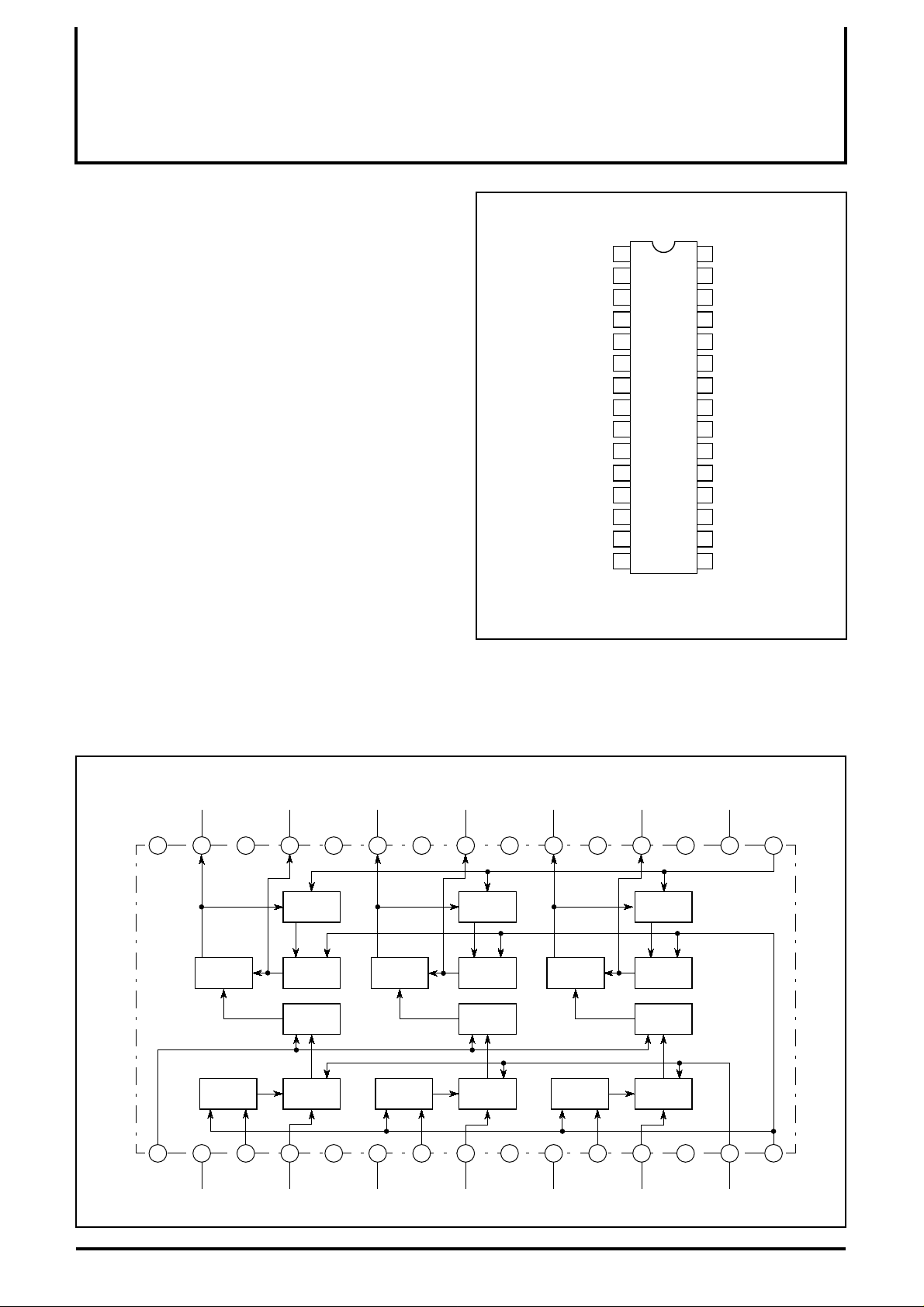
PIN CONFIGURATION (TOP VIEW)
CC1 (B)
CC1 (G)
CC1 (R)
CP IN
1
2
3
4
7
8
12
13
14 17
15 16
OSD BLK IN GND
V
INPUT (B)
SUB CONTRAST (B)
GND1 (B)
V
INPUT (G)
)
SUB CONTRAST (G)
GND1 (G)
V
INPUT (R)
SUB CONTRAST (R)
GND1 (R)
MAIN CONTRAST
Outline 30P4B
30
29
28
27
265
256
M52733SP
24
23
229
2110
2011
19
18
OUTPUT (B)
V
CC2 (B)
HOLD (B)
GND2 (B)
OUTPUT (G)
CC2 (G)
V
HOLD (G)
GND2 (G)
OUTPUT (R)
V
CC2 (R)
HOLD (R)
NC
GND2 (R)
BRIGHTNESS
NC : NO CONNECTION
RECOMMENDED OPERATING CONDITION
Supply voltage range....................................................11.5 to 12.5V
Rated supply voltage................................................................12.0V
BLOCK DIAGRAM
OUTPUT (B)
GND
HOLD (B) OUTPUT (R)
CC2 (B)
V
2930
28 2627 25 24 2021 19 171823 22
Brightness
B
AMP
Blanking
B
Clamp
Contrast
GND2 (B)
B
B
Hold
B
B
OUTPUT (G)
AMP
Clamp
VCC2 (G)
G
G
HOLD (G)
Brightness
Hold
Blanking
Contrast
GND2 (G)
G
G
G
G
V
R
AMP
R
Clamp
CC2 (R)
HOLD (R)
Brightness
Hold
Blanking
Contrast
GND2 (R)
NC
R
R
R
R
BRIGHTNESS
16
13245 98101211 13 1467
OSD BLK IN
INPUT (B) INPUT (R)GND1 (G)
VCC1 (B)
SUB CONTRAST
INPUT (G)GND1 (B)
SUB CONTRAST
V
CC1 (R)VCC1 (G)
SUB CONTRAST
(R) (G) (B)
MAIN CONTRAST
15
CP INGND1 (R)
1
Page 2

°
°
±
− a − a −
a −
∆
−
∆
−
∆
−
−
−
∆
−
−
∆
−
∆
− a − a −
∆
MITSUBISHI ICs (Monitor)
M52733SP
3-CHANNEL VIDEO AMPLIFICATION WITH OSD BLANKING
ABSOLUTE MAXIMUM RATINGS
(Ta=25 ° C)
Symbol Parameter Ratings Unit
V
CC
P
d
T
opr
T
stg
V
opr
V
opr’
Surge Electrostatic discharge
ELECTRICAL CHARACTERISTICS
Symbol Parameter
CC
I
Vomax Output dynamic range
Vimax Maximum input
Gv Maximum gain
Supply voltage 13.0 V
Power dissipation 1736 mW
Ambient temperature -20 to +85
Storage temperature -40 to +150
C
C
Recommended supply voltage 12.0 V
Recommended supply voltage range 11.5 to 12.5 V
200 V
CC
(V
=12V , Ta=25 ° C, unless otherwise noted)
Test conditions
Test
point
Circuit current A
T.P.29
T.P.25
T.P.21
T.P.29
T.P.25
T.P.21
T.P.29
T.P.25
T.P.21
SW11
(s)
R-ch
a
b
SG6bSG6bSG6
b
SG6bSG6bSG6
b
SG6bSG6bSG6
Input
SW7
G-ch
External power supply (V)
SW3
V4 V14 V16 SW1 SW15 Min. Typ. Max.
B-ch
555
55
Variable
5 2.5 1
552
Pulse input
a
b
−
SG5
b
SG5
a
b
SG5
a
b
−
SG5
Limits
60 83 123 mA
5.8 6.8 9.0 V
1 1.8
15 17 20 dB
Gv Rrlative maximum gain Relative to measured values above 0.8 1 1.2
V
V
V
CR1
CR1
V
CR2
V
CR2
SCR1
Contrast control
characteristics (typical)
Contrast control relative
characteristics (typical)
Contrast control
characteristics
(minimum)
Contrast control relative
characteristics (minimum)
Sub contrast control
characteristics (typical)
T.P.29
T.P.25
SG6bSG6bSG6
T.P.21
T.P.29
T.P.25
SG6bSG6bSG6
T.P.21
T.P.29
T.P.25
SG6bSG6bSG6
T.P.21
b
542
a
−
b
14 15.5 17 dB
SG5
Relative to measured values above 0.8 1 1.2
b
512
a
−
b
0.3 0.6 0.9 V
SG5
Relative to measured values above 0.8 1 1.2
b
452
a
−
b
14 15.5 17 dB
SG5
Sub contrast control
V
SCR1
relative characteristics
Relative to measured values above 0.8 1 1.2
(typical)
V
V
V
SCR2
V
SCR2
SCR3
V
SCR3
B1
B1
V
Sub contrast control
characteristics
(minimum)
Sub contrast control relative
characteristics (minimum)
Contrast/sub contrast
control characteristics
(typical)
Contrast/sub contrast
control relative
characteristics (typical)
Brightness control
characteristics
(maximum)
Brightness control relative
characteristics (maximum)
T.P.29
T.P.25
SG6bSG6bSG6
T.P.21
T.P.29
T.P.25
SG6bSG6bSG6
T.P.21
T.P.29
T.P.25
T.P.21
b
152
a
−
b
0.5 0.9 1.3 V
SG5
Relative to measured values above 0.8 1 1.2
b
332
a
−
b
0.8 1.5 2.2 V
SG5
Relative to measured values above 0.8 1 1.2
a
554
a
−
b
3.0 3.6 4.2 V
SG5
Relative to measured values above -0.3 0 0.3 V
Unit
P-P
P-P
V
P-P
P-P
P-P
2
Page 3

a − a −
∆
− a − a −
−
− a − a −
∆
∆
a − a −
MITSUBISHI ICs (Monitor)
M52733SP
3-CHANNEL VIDEO AMPLIFICATION WITH OSD BLANKING
∆
a − a −
∆
− a −
− a −
ELECTRICAL CHARACTERISTICS
Symbol Parameter
B2
V
B2
V
Brightness control
characteristics (typical)
Brightness control relative
characteristics (typical)
Brightness control
B3
V
characteristics
(minimum)
B3
V
Brightness control relative
characteristics (minimum)
Frequency
F
C1
characteristics 1
(f=50MHz)
F
C1
Frequency relative
characteristics 1 (f=50MHz)
Frequency
F
C1’
characteristics 1
(f=130MHz;maximum)
C1’
F
Frequency relative
characteristics 1
(f=130MHz;maximum)
Frequency
F
C2
characteristics 2
(f=130MHz; maximum)
Frequency relative
F
C2’
characteristics 2
(f=130MHz; maximum)
C.T.1 Crosstalk 1 (f=50MHz)
C.T.1’ Crosstalk 1 (f=130MHz)
C.T.2 Crosstalk 2 (f=50MHz)
C.T.2’ Crosstalk 2 (f=130MHz)
C.T.3 Crosstalk 3 (f=50MHz)
C.T.3’ Crosstalk 3 (f=130MHz)
Tr Pulse characteristics 1
Tf Pulse characteristics 2
V14th
W14
Clamp pulse threshold
voltage
Clamp pulse minimum
width
Pedestal voltage
DCH
P
temperatere
characteristics1
Test
point
(s)
T.P.29
T.P.25
T.P.21
T.P.29
T.P.25
T.P.21
T.P.29
T.P.25
T.P.21
T.P.29
T.P.25
T.P.21
T.P.29
T.P.25
T.P.21
T.P.29
T.P.25
T.P.21
T.P.29
T.P.25
T.P.21
T.P.29
T.P.25
T.P.21
T.P.29
T.P.25
T.P.21
T.P.29
T.P.25
T.P.21
T.P.29
T.P.25
T.P.21
T.P.29
T.P.25
T.P.21
T.P.29
T.P.25
T.P.21
T.P.29
T.P.25
T.P.21
T.P.29
T.P.25
T.P.21
T.P.29
T.P.25
T.P.21
(cont.)
Input
SW11
SW7
R-ch
G-ch
a
Relative to measured values above -0.3 0 0.3 V
a
Relative to measured values above -0.3 0 0.3 V
b
SG2bSG2bSG2
Relative to measured values above -1 0 1 dB
b
SG3bSG3bSG3
Relative to measured values above -1 0 1 dB
b
SG3bSG3bSG3
Relative to measured values above -1 0 1 dB
b
a
SG2
b
a
SG3
a
−bSG2a−
a
−bSG3a−
a
a
−
−bSG2
a
a
−
−bSG3
b
SG4bSG4bSG4
b
SG4bSG4bSG4
a
a
−
−
a
a
−
−
b
SG6bSG6bSG6
Test conditions
External power supply (V
SW3
V4 V14 V16 SW1 SW15 Min. Typ. Max.
B-ch
5 5 2.5
551
5 2.5 V
5 2.5 V
5 1.5 V
55V
55V
55V
55V
55V
55V
5 3.3 2
5 3.3 2
a
552
−
a
552
−
552
)
T
T
T
T
T
T
T
T
T
Pulse input
a
b
SG5
a
b
−
SG5
a
a
−
−
a
a
−
−
a
a
−
−
a
a
−
−
a
a
−
−
a
a
−
−
a
−bSG5
a
−bSG5
a
b
−
SG5
a
b
−
SG5
a
b
−
SG5
1.7 2.3 2.9 V
0.5 0.9 1.3 V
-2.5 -1 3 dB
-3 -2 3 dB
-3 0 3 dB
−
− -20 -15 dB
− -30 -20 dB
− -20 -15 dB
− -30 -20 dB
− -20 -15 dB
− 3 7 nsec
− 4 8 nsec
1.0 1.5 2.0 V
− 0.1 0.5 µsec
-0.3 0 0.3 V
Limits
Unit
-30 -20 dB
DC
DC
3
Page 4
3-CHANNEL VIDEO AMPLIFICATION WITH OSD BLANKING
ELECTRICAL CHARACTERISTICS (cont.)
Symbol Parameter
Pedestal voltage
DCL
P
V1th
temperatere
characteristics2
BLK input threshold
voltage
Test
point
(s)
T.P.29
T.P.25
T.P.21
T.P.29
T.P.25
T.P.21
Input
SW11
SW7
G-ch
SW3
B-ch
R-ch
b
SG6bSG6bSG6
b
SG6bSG6bSG6
ELECTRICAL CHARACTERISTICS TEST METHOD
1. Because a description of signal input pin and pulse input pin
switch numbers is already given in Supplementary Table, only
external power supply switch numbers are included in the notes
below.
Sub contrast voltages V4, V8 and V12 are always set to the
same voltage, therefore only V4 is referred to in Supplementary
Table.
CC Circuit current
I
Measuring conditions are as listed in Supplementary Table.
Measured with an ammeter At test point A when SW A is set to b.
MITSUBISHI ICs (Monitor)
M52733SP
Test conditions
External power supply (V)
Pulse input
V4 V14 V16 SW1 SW15 Min. Typ. Max.
a
552
552
3. After setting V
TR (VTG or VTB), increase the SG6 amplitude
SG7bSG5
−
b
b
SG5
gradually , starting from 700mV. Measure the amplitude when the
top and bottom of the wavef orm output at T.P21 (25 or 29) starts
becoming distorted synchronously.
Vimax Maximum input
Measuring conditions are the same as those used above, except
that the setting of V14 is changed to 2.5V as specified in
Supplementary Table. Increase the input signal amplitude gradually,
starting from 700mV
P-P. Measure the amplitude when the output
signal starts becoming distorted.
Limits
-0.3 0 0.3 V
1.7 2.5 3.5 V
Unit
DC
DC
Vomax Output dynamic range
Voltage V16 is varied as described below:
1. Increase V16 gradually while inputting SG6 to pin 11 (7 or 3).
Measure the voltage when the top of the waveform output at
T.P21 (25 or 29) is distorted. The voltage is called V
TR1 (VTG1 or
VTB1). Next, decrease V16 gradually, and measure the voltage
when the bottom of the waveform output at T.P29 (25 or 21) is
distorted. The voltage is called V
(V)
5.0
0.0
2. Voltage V
Waveform Output at T.P21
(Identical to output at T.P25 and T.P29.)
T (VTR, VTG and VTB) is calculated by the equation
TR2 (VTG2 or VTB2).
below:
V
TR (VTG, VTB)=
VTR1 (VTG1, VTB1) + VTR2 (VTG1, VTB1)
2
Gv Maximum gain
∆Gv Relative maximum gain
1. Input SG6 to pin 11 (7 or 3), and read the amplitude at output
T.P21 (25 or 29). The amplitude is called V
OR1 (VOG1 or VOB1) .
2. Maximum gain GV is calculated by the equation below:
V=20LOG
G
OR1 (VOG1, VOB1)
V
0.7
[VP-P]
[V
P-P]
3. Relative maximum gain ∆G is calculated by the equation below:
∆G
V=VOR1/VOG1, V OG1/VOB1, V OB1/VOR1
VCR1 Contrast control characteristics (typical)
∆V
CR1 Contrast control relative characteristics (typical)
1. Measuring conditions are as given in Supplementary Table.
The setting of V14 is changed to 4V.
2. Measure the amplitude output at T.P21 (25 or 29). The measured
value is called VOR2 (VOG2 or VOB2).
3. Contrast control characteristics VCR1 and relative characteristics
∆VCR1 are calculated, respectively, by the equations below:
V
∆V
V
CR1=20LOG
CR1=VOR2/VOG2, V OG2/VOB2, V OB2/VOR2
OR2 (VOG2, VOB2)
0.7
[VP-P]
[V
P-P]
Use relevant voltages, depending on the pin at which the
waveform is output; specifically, use V
TR1 when it is output at
T .P21; VTG1, at T.P25, and VTB, at T.P29.
4
Page 5

MITSUBISHI ICs (Monitor)
M52733SP
3-CHANNEL VIDEO AMPLIFICATION WITH OSD BLANKING
VCR2 Contrast control characteristics (minimum)
∆V
CR2 Contrast control relative characteristics (minimum)
1. Measuring conditions are as given in Supplementary Table.
The setting of V14 is changed to 1.0V.
2. Measure the amplitude output at T.P21 (25 or 29). The measured
value is called VOR3 (VOG3 or VOB3), and is treated as VCR2.
3. Contrast control relative characteristics ∆VCR2 are calculated by
the equation below:
∆V
CR2=VOR3/VOG3, V OG3/VOB3, V OB3/VOR3
VSCR1 Sub contrast control characteristics (typical)
∆V
SCR1 Sub contrast control relative characteristics (typical)
1. Set V4, V8 and V12 to 4.0V. Other conditions are as given in
Supplementary T able.
2. Measure the amplitude output at T .P21 (25 or 29). The measured
value is called VOR4 (VOG4 or VOB4).
3. Sub contrast control characteristics VSCR1 and relative
characteristics ∆VSCR1 are calculated, respectively, by the
equations below:
V
∆V
OR4 (VOG4, VOB4)
SCR1=20LOG
SCR1=VOR4/VOG4, V OG4/VOB4, V OB4/VOR4
V
0.7
[VP-P]
[V
P-P]
VSCR2 Sub contrast control characteristics (minimum)
∆V
SCR2 Sub contrast control relative characteristics (minimum)
1. Set V4, V8 and V12 to 1.0V. Other conditions are as given in
Supplementary T able.
2. Measure the amplitude output at T .P21 (25 or 29). The measured
value is called VOR5 (VOG5 or VOB5).
3. Relative characteristics ∆V
SCR2 are calculated by the equation
below:
∆VSCR2=VOR5/VOG5, VOG5/VOB5, V OB5/V OR5
VSCR3 Contrast/sub contrast control characteristics (typical)
∆V
SCR3 Contrast/sub contrast control relative
characteristics (typical)
1. Set V4, V8, V12 and V14 to 3.0V. Other conditions are as given
in Supplementary Table.
2. Measure the amplitude at T.P21 (25 or 29). The measured value
is called VOR6 (VOG6 or VOB6).
V
CR3=20LOG
VOR6 (VOG6, V OB6)
0.7
[VP-P]
P-P]
[V
VB1 Brightness control characteristics (maximum)
∆V
B1 Brightness control relative characteristics (maximum)
1. Measuring conditions are as given in Supplementary Table.
2. Measure the output at T.P21 (25 or 29) with a voltmeter.
The measured value is called VOR7 (V OG7 or V OB7), and is treated
as VB1.
3. T o obtain brightness control relative characteristics, calculate the
difference in the output between the channels, using VOR7, V OG7
OB7.
and V
∆VB1=VOR7-VOG7 [mV]
=VOG7-VOB7
=VOB7-VOR7
VB2 Brightness control characteristics (typical)
∆V
B2 Brightness control relative characteristics (typical)
1. Measuring conditions are as given in Supplementary Table.
2. Measure the output at T.P21 (25 or 29) with a voltmeter.
The measured value is called VOR7' (VOG7' or VOB7'), and is
treated as VB2.
3. To obtain brightness control relative characteristics (∆VB2),
calculate the difference in the output between the channels,
using VOR7', V OG7', and VOB7'.
∆VB2 =VOR7'-VOG7' [mV]
=VOG7'-VOB7'
=VOB7'-VOR7'
VB3 Brightness control characteristics (minimum)
∆V
B3 Brightness control relative characteristics (minimum)
1. Measuring conditions are as given in Supplementary Table.
2. Measure the output at T.P21 (25 or 29) with a voltmeter.
The measured value is called VOR7" (VOG7" or VOB7"), and is
treated as VB2.
3. To obtain brightness control relative characteristics (∆VB3),
calculate the difference in the output between the channels,
using VOR7", V OG7" and VOB7".
∆VB3 =VOR7''-VOG7'' [mV]
=VOG7''-VOB7''
=VOB7''-VOR7''
∆V
5
CR3=VOR6/VOG6, V OG6/VOB6, V OB6/VOR6
FC1 Frequency characteristics1 (f=50MHz)
∆FC1 Frequency relative characteristics1 (f=50MHz)
FC1' Frequency characteristics1 (f=130MHz; maximum)
∆FC1' Frequency relative characteristics1
(f=130MHz; maximum)
1. Measuring conditions are as given in Supplementary Table.
2. SG2 and SG3 are input. The amplitude of the waveform output at
T.P21 (25 or 29) is measured by the same procedure as in G
V,
∆GV.
Page 6

MITSUBISHI ICs (Monitor)
M52733SP
3-CHANNEL VIDEO AMPLIFICATION WITH OSD BLANKING
3. Supposing that the measured value is treated as amplitude VOR1
(VOG1 or V OB1) when SG1 is input, as V OR8 (V OG8 or V OB8) when
SG2 is input, or as VOR9 (VOG9 or VOB9) when SG3 is input,
frequency characteristics FC1 and FC1' are calculated as follows:
OR8 (VOG8, VOB8) [VP-P]
FC1=20LOG
FC1'=20LOG
4. Frequency relative band widths ∆F
difference in F
C2 Frequency characteristics2 (f=130MHz; maximum)
F
V
V
OR1 (VOG1, VOB1) [VP-P]
VOR9 (VOG9, VOB9) [VP-P]
V
OR1 (VOG1, VOB1) [VP-P]
C1 and ∆FC1' are equal to the
C1 and FC1', respectively, between the channels.
∆FC2' Frequency relative characteristics2
(f=130MHz; maximum)
Measuring conditions and procedure are the same as described in
F
C1, ∆FC1, FC1', ∆FC1', except that CONTRAST (V14) is turned
down to 1.5V.
C.T.1 Crosstalk1 (f=50MHz)
C.T.1' Crosstalk1 (f=130MHz)
1. Measuring conditions are as given in Supplementary Table.
2. Input SG2 (or SG3) to pin 11 (R-ch) only, and then measure the
waveform amplitude output at T.P21 (25 or 29). The measured
value is called VOR, VOG and or VOB respectively.
3. Crosstalk C.T. 1 is calculated by the equation below:
C.T.1 =20LOG
(C.T.1')
OG or VOB [VP-P]
OR [VP-P]
V
[dB]
V
C.T.2 Crosstalk2 (f=50MHz)
C.T.2' Crosstalk2 (f=130MHz)
1. Change the input pin from pin 11 (R-ch) to pin 7 (G-ch), and
measure the output in the same way as in C.T.1, C.T.1'.
2. Crosstalk C.T. 2 is calculated by the equation below:
C.T.2 =20LOG
(C.T.2')
VOR or VOB [VP-P]
OG [VP-P]
V
[dB]
C.T.3 Crosstalk3 (f=50MHz)
C.T.3' Crosstalk3 (f=130MHz)
1. Change the input pin from pin 11 (R-ch) to pin 3 (B-ch), and
measure the output in the same way as in C.T.1, C.T.1'.
2. Crosstalk C.T. 3 is calculated by the equation below:
C.T.3 =20LOG
(C.T.3')
VOR or VOG [VP-P]
OB [VP-P]
V
[dB]
Tr Pulse characteristics1
Tf Pulse characteristics2
1. Measuring conditions are as given in Supplementary Table.
2. Measure the time needed for the input pulse to rise from 10% to
90% (Tr1) and to fall from 90% to 10% (Tf1) with an active prove.
3. Measure the time needed for the output pulse to rise from 10%
to 90% (Tr2) and to fall from 90% to 10% (Tf2) with an active
prove.
4. Pulse characteristics Tr and Tf are calculated by the equation
below:
Tr (nsec)= (Tr2)2-(Tr1)
Tf (nsec)= (Tf2)2-(Tf1)
2
2
100%
90%
10%
0%
Tr
Tf
V14th Clamp pulse threshold voltage
1. Measuring conditions are as given in Supplementary Table.
2. Turn down the SG5 input level gradually, monitoring the output
(about 2.0 VDC). Measure the SG5 input level when the output
reaches 0V.
W14 Clamp pulse minimum width
Under the same conditions as given in V14th, reduce the SG5 pulse
width gradually, monitoring the output. Measure the SG5 pulse
width when the output reaches 0V.
P
DCH Pedestal voltage temperatere characteristics1
PDCL Pedestal voltage temperatere characteristics2
1. Measuring conditions are as given in Supplementary Table.
2. Measure the pedestal voltage at room temperature.
The measured value is called P
DC1.
3. Measure the pedestal voltage at temperatures of -20°C and
85°C. The measured value is called, respectively, PDC2 and
PDC3.
4. PDCH=PDC1 - PDC2
PDCL=PDC1 - PDC3
V1th BLK input threshold voltage
1. Measuring conditions are as given in Supplementary Table.
2. Make sure that signals are not being output synchronously with
SG7 (blanking period).
3. Reduce the SG7 input level gradually, monitoring output.
Measure the SG7 level when the blanking period disappears.
The measured value is called V1th.
6
Page 7

3-CHANNEL VIDEO AMPLIFICATION WITH OSD BLANKING
INPUT SIGNAL
SG No. Signals
Sine wave of amplitude 0.7VP-P (f=1MHz)
MITSUBISHI ICs (Monitor)
M52733SP
SG1
SG2 Sine wave with amplitude of 0.7V
SG3 Sine wave with amplitude of 0.7VP-P (f=130MHz)
Pulse with amplitude of 0.7V
Pulses which are synchronous with SG4 pedestal portion
SG4
Pulses which are synchronous with standard video step waveform pedestal portion:
amplitude, 2.0VP-P; and pulse width, 3.0µs (pulse width and amplitude sometimes variable)
SG5
0V
SG6
Standard
video step
waveform
P-P (f=50MHz)
P-P (f=30kHz, duty=50%)
3.0µs
0.7VP-P
0.7VP-P
2.0VP-P
3.0µs
SG7
OSD BLK
signals
Video signal with amplitude of 0.7V
Pulses which are synchronous with standard video step waveform’s video portions: amplitude, 4.0VP-P; and pulse width, 25µs
P-P (f=30kHz, amplitude sometimes variable)
4V
0V
7
Page 8

TEST CIRCUIT
MITSUBISHI ICs (Monitor)
M52733SP
3-CHANNEL VIDEO AMPLIFICATION WITH OSD BLANKING
680
29
30
2.2µ
28
2627
GND
680
25
2.2µ
23
24 2021 19 1718 16
VCCVCC
22
GND
680
2.2µ
NC
V16
GNDVCC
M52733SP
VCC GND VCC GND VCC GND
13
2
SW1
b
a
SW3
100µ
SG1
SG2
SG3
SG4
SG6
b
SG7
0.01µ
A
b
a
SWA
12V
4
0.01µ
a
6
598101211 13 14
SW7
b
7
0.01µ
0.01µ
SW11
a
b
V12V8V4
a
Units Resistance : Ω
15
V14
SW15
b
a
SG4
Capacitance : F
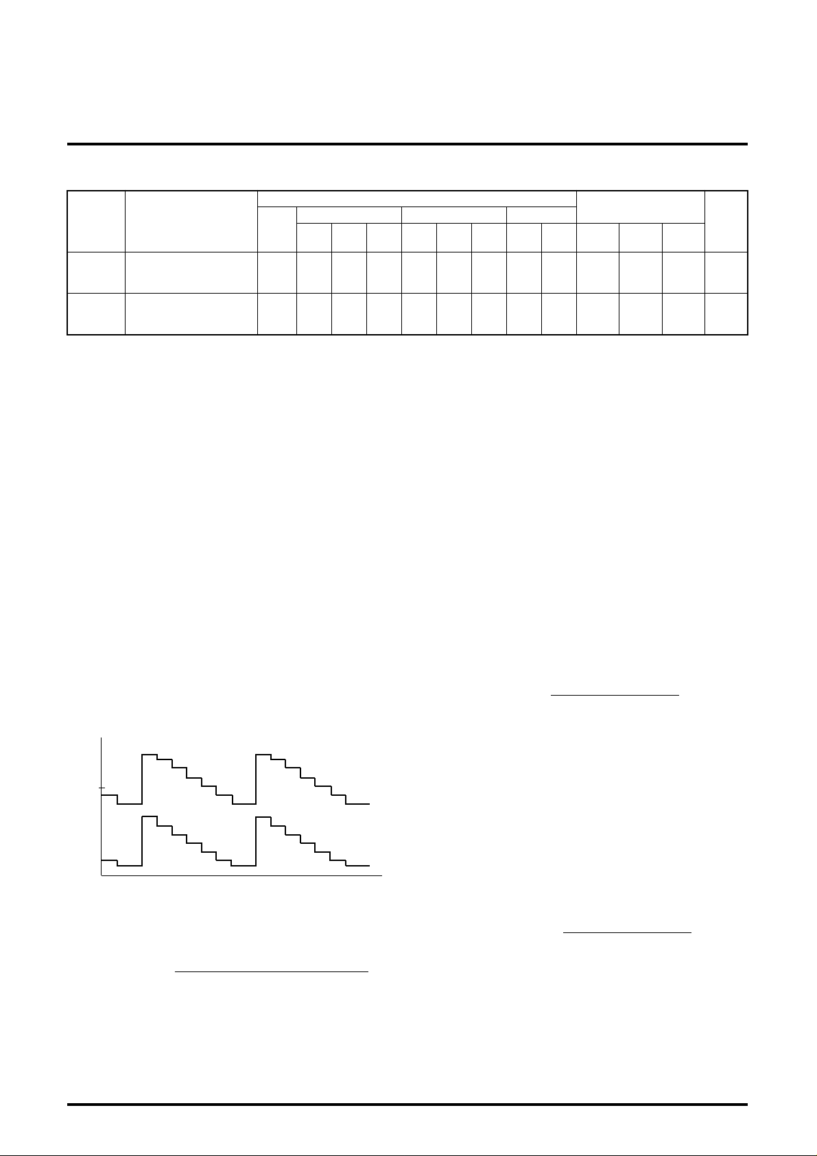
TYPICAL CHARACTERISTICS
THERMAL DERATING (MAXIMUM RATING)
1800
1600
1400
1200
1000
800
600
400
200
POWER DISSIPATION Pd (mW)
0 25 50 75 100 125
AMBIENT TEMPERATURE Ta (°C)
85
150-20
8
Page 9

APPLICATION EXAMPLE 1
110V
MITSUBISHI ICs (Monitor)
M52733SP
3-CHANNEL VIDEO AMPLIFICATION WITH OSD BLANKING
CRT
DC CLAMP
14k
200
680
29
30
132
50k50k50k
14k
200
680
27
25
2628
24 2021 19 1718
14k
200
680
23
22
M52733SP
4
0 to 5V
6
598101211 13 15
7
0 to 5V
0 to 5V
OSD IN
0 to 5V
NC
16
14
0 to 5V
12V CLAMPINPUT
OSD BLK
IN
9
(B)
INPUT
(G)
INPUT
(R)
Units Resistance : Ω
Capacitance : F
Page 10

APPLICATION EXAMPLE 2
110V
MITSUBISHI ICs (Monitor)
M52733SP
3-CHANNEL VIDEO AMPLIFICATION WITH OSD BLANKING
CRT
DC CLAMP
680
29
30
132
680
27
25
2628
23
24 2021 19 1718
22
680
M52733SP
4
0 to 5V
6
598101211 13 15
7
0 to 5V
0 to 5V
OSD IN
0 to 5V
NC
16
14
0 to 5V
12V CLAMPINPUT
OSD BLK
IN
(B)
INPUT
(G)
INPUT
(R)
Units Resistance : Ω
Capacitance : F
10
Page 11

MITSUBISHI ICs (Monitor)
M52733SP
3-CHANNEL VIDEO AMPLIFICATION WITH OSD BLANKING
DESCRIPTION OF PIN
Pin No. Name DC voltage (V ) Peripheral circuit of pins Description of function
CC
V
1 OSD BLK IN −
2
6
10
3
7
11
V
CC (B-ch)
VCC (G-ch)
VCC (R-ch)
INPUT (B)
INPUT (G)
INPUT (R)
B-ch
G-ch
1
0.9mA
12 −
2k
2.5
0.24mA
CP
⋅Input pulses of minimum
3V.
3 to 5V
1V
maximum
2.5V
⋅Connected to GND if not
used.
GND
⋅Apply equivalent
voltage to 3 channels.
VCC
2k
⋅Clamped to about 2.5V
due to clamp pulses
from pin 18.
⋅Input at low impedance.
2.5V
GND
4
Subcontrast
(B)
8
Subcontrast
(G)
12
Subcontrast
(R)
14
Main
contrast
5, 26
9, 22
13, 17
30
GND (B-ch)
GND (G-ch)
GND (R-ch)
GND
15 CP IN −
1.5k
2.5
23.5k
GND −
18
41k
2.5V
VCC
GND
2.2V
⋅Use at maximum 5V
for stable operation.
VCC
⋅Input pulses of minimum
2.5V.
⋅Input at low impedance.
GND
2.5V
minimum
0.5V
maximum
11
Page 12

MITSUBISHI ICs (Monitor)
Pin 21
Pin 25
Pin 29
Pin 20
Pin 24
Pin 28
50
M52733SP
3-CHANNEL VIDEO AMPLIFICATION WITH OSD BLANKING
DESCRIPTION OF PIN (CONT.)
Pin No. Name DC voltage (V ) Peripheral circuit of pins Description of function
VCC
20.3k
16
19
23
27
20
24
28
21
25
29
Main
brightness
Hold (R)
Hold (G)
Hold (B)
CC2 (R)
V
VCC2 (G)
VCC2 (B)
OUTPUT (R)
OUTPUT (G)
OUTPUT (B)
−
Variable
Apply 12
Variable
B-ch
G-ch
19
GND
VCC
1k
⋅A capacity is needed on
the GND side.
0.2mA
GND
⋅Used to supply power to
output emitter follower
only.
⋅Apply equivalent voltage
to 3 channels.
⋅A resistor is needed on
the GND side.
Set discretionally to
maximum 15mA,
depending on the
required driving capacity.
12
 Loading...