

Page 1
MITSUBISHI ICs (Monitor)
M52732SP
3-CHANNEL VIDEO AMPLIFICA TION
DESCRIPTION
The M52732SP is a semiconductor integrated circuit that has 3channels of built-in amplifiers in the broad-band video amplifier
having a 75MHz band. Every channel is provided with a broad-band
amplifier, contrast control (main and sub), and brightness control. It
accordingly has an optimal configuration for use with high
resolution color display monitors.
FEATURES
It realize low power dissipation so that 3-channels are built in.
•
(V
=12V, I
CC
Input..........................................................................0.7V
•
Output.....................................................................4.5V
Frequency band.................................................75MHz (at 3V
•
To adjust contrast, two types of controls are provided, main and
=63mA)
CC
P-P
P-P
(typ.)
(max.)
P-P
sub.
The main controls adjusts 3-channels of contrast concurrently.
The sub contrast controls adjusts either channel independentry.
APPLICATION
Display monitor
RECOMMENDED OPERATING CONDITION
Supply voltage range....................................................11.5 to 12.5V
Rated supply voltage................................................................12.0V
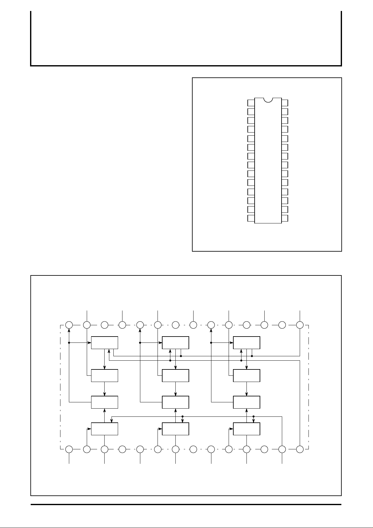
PIN CONFIGURATION (TOP VIEW)
CC (B) OUTPUT (B)
V
INPUT (B)
SUB CONTRAST
CONTROL (B)
GND (B)
V
INPUT (G)
SUB CONTRAST
CONTROL (G)
GND (G)
)
SUB CONTRAST
MAIN CONTRAST
V
INPUT (R)
CONTROL (R)
GND (R)
CONTROL
1
2
3
4
CC (G)
5
6
7
8
CC (R)
9
10
11
12
13
14 15
CP IN
Outline 28P4B
28
27
26
25
24
M52732SP
23
22
21
20
19
18
17
16
HOLD (B)
NC
GND (B)
OUTPUT (G)
HOLD (G)
NC
GND (G)
OUTPUT (R)
HOLD (R)
NC
GND (R)
CC
V
BRIGHTNESS
CONTROL
NC : NO CONNECTION
BLOCK DIAGRAM
OUTPUT (B) OUTPUT (R)
28 2627 25 24 2021 19 1718 16 1523 22
13245 98101211 13 1467
INPUT (B) INPUT (R)GND (G)
VCC (B)
GND (B) HOLD (R)HOLD (B)
NC
B-ch
Brt
B-ch
Hold
B-ch
Amp
B-ch
CONTRAST
SUB CONTRAST
HOLD(G)
OUTPUT (G) NC
G-ch
Brt
G-ch
Hold
G-ch
Amp
G-ch
CONTRAST
INPUT (G)GND (B)
SUB CONTRAST
GND (G)
GND (R)
NC
R-ch
Brt
R-ch
Hold
R-ch
Amp
R-ch
CONTRAST
CC (R)VCC (G)
V
SUB CONTRAST
BRIGHTNESS
CONTROL
CC
V
CP INGND (R)
MAIN CONTRAST
CONTROLCONTROL (R)CONTROL (G)CONTROL (B)
1
Page 2

°
°
±
− a − a −
a −
a −
a −
∆
−
a −
∆
a −
∆
−
∆
∆
−
∆
−
−
−
− a − a −
∆
MITSUBISHI ICs (Monitor)
M52732SP
3-CHANNEL VIDEO AMPLIFICA TION
ABSOLUTE MAXIMUM RATINGS
(Ta=25 ° C)
Symbol Parameter Ratings Unit
V
CC
P
d
T
opr
T
stg
V
opr
V
opr’
Surge Electrostatic discharge
ELECTRICAL CHARACTERISTICS
Supply voltage 13.0 V
Power dissipation 1580 mW
Ambient temperature -20 to +85
Storage temperature -40 to +150
C
C
Recommended supply voltage 12.0 V
Recommended supply voltage range 11.5 to 12.5 V
200 V
(V
CC
=12V , Ta=25 ° C, unless otherwise noted)
Test conditions
Limits
45 72 110 mA
5.8 6.8 9.0 V
1.9 2.4 2.9 V
13 17 20 dB
Symbol Parameter
CC
I
Circuit current A
Vomax Output dynamic range
Vimax Maximum input
Gv Maximum gain
Test
point (s)
T.P.20
T.P.24
T.P.28
T.P.20
T.P.24
T.P.28
T.P.20
T.P.24
T.P.28
Input
SW10
R-ch
SW6
G-ch
SW2
B-ch
a
b
SG1bSG1bSG1
b
SG1bSG1bSG1
b
SG1bSG1bSG1
External power supply (V)
Pulse
input
V3 V13 V15 SW14 Min. Typ. Max.
12 12 5
12 12
12 6
Variable
Variable
12 12 V
b
SG6
T
Gv Relative maximum gain Relative to measured values above 0.8 1 1.2
V
V
V
CR1
V
CR1
CR2
V
CR2
SCR1
Contrast control
characteristics (typical)
Contrast control relative
characteristics (typical)
Contrast control
characteristics
(minimum)
Contrast control relative
characteristics (minimum)
Sub contrast control
characteristics (typical)
T.P.20
T.P.24
T.P.28
T.P.20
T.P.24
T.P.28
T.P.20
T.P.24
T.P.28
b
SG1bSG1bSG1
Relative to measured values above 0.8 1 1.2
b
SG1bSG1bSG1
Relative to measured values above 0.8 1 1.3
b
SG1bSG1bSG1
12 6 V
12 3.5 V
612V
T
T
T
4.0 7.4 10.1 dB
5 30 70 mV
a
9.9 14 18.1 dB
−
Sub contrast control
V
SCR1
relative characteristics
Relative to measured values above 0.8 1 1.2
(typical)
V
V
V
SCR2
V
SCR2
CR2
V
CR2
B1
B1
V
Sub contrast control
characteristics
(minimum)
Sub contrast control relative
characteristics (minimum)
Contrast/sub contrast
control characteristics
(typical)
Contrast/sub contrast
control relative
characteristics (typical)
Brightness control
characteristics
(maximum)
Brightness control relative
characteristics (maximum)
T.P.20
T.P.24
T.P.28
T.P.20
T.P.24
T.P.28
T.P.20
T.P.24
T.P.28
b
SG1bSG1bSG1
Relative to measured values above 0.8 1 1.2
b
SG1bSG1bSG1
Relative to measured values above 0.8 1 1.2
a
Relative to measured values above -100 0 100 mV
312V
66V
T
T
12 12 5.5
a
50 300 600 mV
−
a
0.9 1.3 1.7 V
−
b
3.6 4.3 5.0 V
SG6
Unit
P-P
P-P
P-P
P-P
P-P
2
Page 3

∆
a −
∆
a −
∆
− a − a −
− a − a −
∆
MITSUBISHI ICs (Monitor)
M52732SP
3-CHANNEL VIDEO AMPLIFICA TION
a −
∆
a −
a
a
− a −
−
−
− a −
ELECTRICAL CHARACTERISTICS
Symbol Parameter
B2
V
B2
V
Brightness control
characteristics (typical)
Brightness control relative
characteristics (typical)
Brightness control
V
B3
characteristics
(minimum)
B3
V
Brightness control relative
characteristics (minimum)
Frequency
F
C1
characteristics 1
(f=50MHz;maximum)
Frequency relative
F
C1
characteristics 1
(f=50MHz;maximum)
Frequency
F
C1’
characteristics 1
(f=75MHz;maximum)
Frequency relative
F
C1’
characteristics 1
(f=75MHz;maximum)
Frequency
F
C2
characteristics 2
(f=50MHz; maximum)
Frequency relative
F
C2’
characteristics 2
(f=75MHz; maximum)
C.T.1 Crosstalk 1 (f=50MHz)
C.T.1’ Crosstalk 1 (f=75MHz)
C.T.2 Crosstalk 2 (f=50MHz)
C.T.2’ Crosstalk 2 (f=75MHz)
C.T.3 Crosstalk 3 (f=50MHz)
C.T.3’ Crosstalk 3 (f=75MHz)
Tr Pulse characteristics 1
Tf Pulse characteristics 2
V14th
W14
Clamp pulse threshold
voltage
Clamp pulse minimum
width
V27 Hold voltage
Test
point (s)
T.P.20
T.P.24
T.P.28
T.P.20
T.P.24
T.P.28
T.P.20
T.P.24
T.P.28
T.P.20
T.P.24
T.P.28
T.P.20
T.P.24
T.P.28
T.P.20
T.P.24
T.P.28
T.P.20
T.P.24
T.P.28
T.P.20
T.P.24
T.P.28
T.P.20
T.P.24
T.P.28
T.P.20
T.P.24
T.P.28
T.P.20
T.P.24
T.P.28
T.P.20
T.P.24
T.P.28
T.P.20
T.P.24
T.P.28
T.P.20
T.P.24
T.P.28
T.P.20
T.P.24
T.P.28
T.P.20
T.P.24
T.P.28
T.P.20
T.P.24
T.P.28
(cont.)
Input
SW10
R-ch
SW6
G-ch
a
Relative to measured values above -100 0 100 mV
a
Relative to measured values above -100 0 100 mV
b
SG3bSG3bSG3
Relative to measured values above -1 0 1 dB
b
SG4bSG4bSG4
Relative to measured values above -1 0 1 dB
b
SG3bSG3bSG3
b
SG4bSG4bSG4
b
a
SG3
b
a
SG4
a
b
SG3
a
−bSG4a−
a
a
−
−bSG3
a
a
−
−bSG4
b
SG5bSG5bSG5
b
SG5bSG5bSG5
a
a
−
−
a
a
−
−
a
a
−
−
Test conditions
External power supply (V)
SW2
B-ch
V3 V13 V15 SW14 Min. Typ. Max.
12 12 5
12 12 4.5
12 7.5 V
12 7.5 V
12 5 V
12 5 V
12 12 V
12 12 V
a
12 12 V
12 12 V
12 12 V
12 12 V
12 7 3
12 7 3
a
12 12 3
−
a
12 12 3
−
a
12 12 3
−
Pulse
input
b
SG6
b
SG6
T
T
T
T
T
−
T
−
a
T
−
a
T
−
a
T
−
a
T
−
b
SG6
b
SG6
b
SG6
b
SG6
b
SG6
Limits
Unit
3.0 3.7 4.4 V
2.5 3.2 4.0 V
-2 0 3 dB
-3 0 3 dB
-0.5 0 3 dB
-0.5 0 3 dB
−
-36 -24 dB
−
-28 -18 dB
− -36 -24 dB
− -28 -18 dB
− -36 -24 dB
− -28 -18 dB
− 3 7 nsec
− 6 9 nsec
0.7 1.5 2.5 V
− 0.3 1.5 µsec
4 5.2 6.4 V
DC
DC
DC
3
Page 4
MITSUBISHI ICs (Monitor)
M52732SP
3-CHANNEL VIDEO AMPLIFICA TION
ELECTRICAL CHARACTERISTICS TEST METHOD
1. About switch numbers (SW Nos.) since those f or the signal and
pulse input pins are listed in Attached Table 1, the following
notes omit them. Only SW Nos. for the e xternal power supply will
be indicated in the Notes.
2. since sub contrast voltges V3, V7, and V11, they are also set to
the same value, so that V3 in attached Table 1 represents all.
CC Circuit current
I
Conditions shall be as indicated in Attached Table 1. Measure
these conditions using ampere meter A with SW1 set to a.
Vomax Output dynamic range
1. Follow the procedure below to set V15.
Input SG1 to pin 10 (pin 6, 2) and raise V15 slowly. Read the
voltage of V15 when the higher peak of output w av eform of T.P20
(T.P24, 28) begins distortion. This voltage is V
Next, reduce V15 slo wly. Read the v oltage of V15 when the low er
peak of output waveform of T.P20 (T.P24, 28) begins distortion.
This voltage is VTR2 (VTG2, VTB2).
(V)
TR1 (VTG1, VTB1)
Gv Maximum gain
∆Gv Relative maximum gain
1. Under conditions in attached Table.
2. Input SG1 to pin 10 (pin 6, 2). Read amplitude of the output at
T.P20 (T.P24, 28), which is VOR1 (VOG1, VOB1).
3. The maximum gain G is:
GV=20LOG
OR1 (VOG1, VOB1)
V
0.7
[VP-P]
[V
P-P]
4. The maximum relative gain ∆G is calculated by the equation
below:
∆G
V=VOR1/VOG1, V OG1/VOB1, V OB1/VOR1
VCR1 Contrast control characteristics (typical)
∆V
CR1 Contrast control relative characteristics (typical)
1. Conditions are identical with those in Attached Table except
setting V13 to 6.0V.
2. Then read amplitude of the output at T.P20 (T.P24, 28), which is
VOR2 (VOG2, V OB2)
3. The contrast control characteristics VCR1 and relative contrast
control characteristics ∆VCR1 are calculated by the equations
below:
CR1=20LOG
V
OR2 (VOG2, VOB2)
V
0.7
[VP-P]
[V
P-P]
5.0
0.0
Waveform output at T.P20
(Identical to output at T.P24 and T.P28.)
From the above result, V
T (VTR, VTG, VTB) is determined as
follows:
V
TR (VTG, VTB)=
VTR1 (VTG1, VTB1) + VTR2 (VTG2, VTB2)
2
Change the procedure according to output pins.
Use V
TR1 when measuring T.P20. Similarly, VTG1 for T .P24, VTB1
for T.P28.
2. Set V15 to VTR (VTG, VTB), then slowly raise SG1 amplitude
starting from 700mV. Measure the output amplitude when the
higher and lower peaks of T.P20 (T.P24, T.P28) output waveform
simultaneously begin distortion.
Vimax Maximum input
Under the conditions in Note 2, vary V13 to 6.7V as indicated in
Attached Table 1, then slowly raise amplitude of the input signal
starting from 700mV
P-P. Read the amplitude of the input signal
when the output signal begins distortion.
∆V
CR1=VOR2/VOG2, V OG2/VOB2, V OB2/VOR2
VCR2 Contrast control characteristics (minimum)
∆V
CR2 Contrast control relative characteristics (minimum)
1. Conditions are identical with those in Attached Table except
setting V13 to 3.0V.
2. Then read amplitude of the output at T.P20 (T.P24, 28), which is
VOR3 (VOG3, V OB3) and also VCR2.
3. The relative contrast control characteristics ∆VCR2 is:
∆VCR2=VOR3/VOG3, VOG3/VOB3, V OB3/VOR3
VSCR1 Sub contrast control characteristics (typical)
∆V
SCR1 Sub contrast control relative characteristics (typical)
1. Conditions are identical with those in Attached Table except
setting V3, V7, and V11 to 6.0V.
2. Then read amplitude of the output at T.P20 (T.P24, 28), which is
VOR4 (VOG4, V OB4).
3. The sub contrast control characteristics VSCR1 and relative sub
contrast control characteristics ∆VSCR1 are:
V
∆V
OR4 (VOG4, VOB4)
SCR1=20LOG
SCR1=VOR4/VOG4, V OG4/VOB4, V OB4/VOR4
V
0.7
[VP-P]
[V
P-P]
4
Page 5

MITSUBISHI ICs (Monitor)
M52732SP
3-CHANNEL VIDEO AMPLIFICA TION
VSCR2 Sub contrast control characteristics (minimum)
∆V
SCR2 Sub contrast control relative characteristics (minimum)
1. Conditions are identical with those in Attached Table expect
setting V3, V7, and V11 to 3.0V.
2. Then read amplitude of the output at T.P20 (T.P24, 28), which is
VOR5 (VOG5, V OB5) and also VSCR2.
3. The relative sub contrast control characteristics ∆VSCR2 is:
∆VSCR2=VOR5/VOG5, VOG5/VOB5, V OB5/VOR5
VCR2 Contrast/sub contrast control characteristics (typical)
∆V
CR2 Contrast/sub contrast control relative
characteristics (typical)
1. Conditions are identical with those in Attached Table expect
setting V13, to 6.0V and V3, V7, and V11 to 6.0V.
2. Then read amplitude of the output at T.P20 (T.P24, 28), which is
VOR6 (VOG6, V OB6).
3. The gain and relative gain when the contrast and sub contrast
are typical, are:
CR3=20LOG
V
OR6 (VOG6, VOB6)
V
0.7
[VP-P]
[V
P-P]
∆VCR3=VOR6/VOG6, VOG6/VOB6, V OB6/VOR6
VB1 Brightness control characteristics (maximum)
∆V
B1 Brightness control relative characteristics (maximum)
1. Under conditions in Attached Table.
2. Then use a voltmeter to measure the output at T.P20 (T.P24, 28),
which is VOR7 (VOG7, VOB7). This value is VB1.
3. In addition, the relative brightness control characteristic is
determined from VOR7, VOG7, and VOB7 b y calculating differences
between each channel.
∆VB1=VOR7-VOG7
=VOG7-VOB7 [mV]
=VOB7-VOR7
VB3 Brightness control characteristics (minimum)
∆V
B3 Brightness control relative characteristics (minimum)
1. Under conditions in Attached Table.
2. Then use a voltmeter to measure the output at T.P20 (T.P24, 28),
which is VOR7'' (VOG7'', VOB7''). This value is VB3.
3. In addition, the relative brightness control characteristic ∆VB3 is
determined from VOR7'', VOG7'', and VOB7'' by calculating
differences between each channel.
B3 =VOR7''-VOG7''
∆V
=VOG7''-VOB7'' [mV]
=VOB7''-VOR7''
FC1 Frequency characteristics1 (f=50MHz; maximum)
∆FC1 Frequency relative characteristics1
(f=50MHz; maximum)
FC1' Frequency characteristics1 (f=75MHz; maximum)
∆FC1' Frequency relative characteristics1
(f=75MHz; maximum)
1. Under conditions in Attached Table.
2. Use SG3 and SG4. Measure amplitude of the output waveform
at T.P20 (T.P24, T.P28) following the procedure in G
V, ∆GV.
3. The frequency characteristics FC1, FC1' are calculated by the
equations below:
FC1=20LOG
FC1'=20LOG
Whre, V
OR8 (VOG8, VOB8) is the output amplitude when inputting
VOR8 (VOG8, VOB8) [VP-P]
V
OR1 (VOG1, VOB1) [VP-P]
VOR9 (VOG9, VOB9) [VP-P]
V
OR1 (VOG1, VOB1) [VP-P]
SG3, and VOR9 (VOG9, VOB9), SG4, which are measured in 2
above. (VOR1 (VOG1, V OB1) is the value measured in GV, ∆GV.)
4. The relative frequency characteristics ∆FC1, ∆FC1' are
determined by calculating differences between each channel's
FC1 and FC1'.
VB2 Brightness control characteristics (typical)
∆V
B2 Brightness control relative characteristics (typical)
1. Under conditions in Attached Table.
2. Then use a voltmeter to measure the output at T.P20 (T.P24, 28),
which is VOR7' (VOG7', VOB7'). This value is VB2.
3. In addition, the relative brightness control characteristic is
determined from VOR7', VOG7', and VOB7' by calculating
differences between each channel.
∆VB2=VOR7'-VOG7'
=VOG7'-VOB7' [mV]
=VOB7'-VOR7'
5
C2 Frequency characteristics2 (f=50MHz; maximum)
F
∆FC2' Frequency relative characteristics2
(f=75MHz; maximum)
The procedure is identical with that in F
C1, ∆FC1, FC1', ∆FC1' except
that the contrast (V13) is reduced to 5.0V.
C.T.1 Crosstalk1 (f=50MHz)
C.T.1' Crosstalk1 (f=75MHz)
1. Under conditions in attached Table.
2. Input SG2 (or SG4) to pin 10 (R-ch) only. Then measure
amplitude of the output wavef orm at T.P20 (T.P24, T.P28), which
are VOR, V OG, and VOB, respectively.
3. Crosstalk C.T. is:
V
C.T. =20LOG
(C.T. ')
OG or VOB [VP-P]
OR [VP-P]
V
[dB]
Page 6

MITSUBISHI ICs (Monitor)
M52732SP
3-CHANNEL VIDEO AMPLIFICA TION
C.T.2 Crosstalk2 (f=50MHz)
C.T.2' Crosstalk2 (f=75MHz)
1. Afterthe input pin from 10 (R-ch) to 6 (G-ch) and read the output
following the procedure in C.T.1, C.T.1'.
2. Crosstalk C.T. is:
C.T. =20LOG
(C.T. ')
OR or VOB [VP-P]
OG [VP-P]
V
[dB]
V
C.T.3 Crosstalk3 (f=50MHz)
C.T.3' Crosstalk3 (f=75MHz)
1. After the input pin from 10 (R-ch) to 2 (B-ch) and read the output
following the procedure in C.T.1, C.T.1'.
2. Crosstalk C.T. is:
C.T. =20LOG
(C.T. ')
VOR or VOB [VP-P]
OG [VP-P]
V
[dB]
Tr Pulse characteristics1
Tf Pulse characteristics2
1. Under conditions in attached Table.
2. Measure 10% to 90% rise Tr1 and fall Tf1 of the input pulse
using an active probe.
3. Next, measure 10% to 90% rise Tr2 and fall Tf2 of the output
pulse using an active probe.
4. Pulse characteristics Tr and Tf are calculated by the equations
below :
2
2
Tr (nsec)= (Tr2)
Tf (nsec)= (Tf2)2-(Tf1)
-(Tr1)
2
V14th Clamp pulse threshold voltage
1. Under conditions in attached Table.
2. Then slowly reduce the level of SG6 monitoring the output
(approx.2.0VDC) and measure the level of SG6 when the output
becomes 0V.
W14 Clamp pulse minimum width
Under the conditions in V14th, slowly reduce the pulse width of
SG6 monitoring the output.
Then measure the pulse width of SG6 when the output becomes
0V.
V27 Hold voltage
1. Under conditions in attached Table.
2. Read T.P19, 23 and 27 with a voltmeter.
0%
100%
90%
10%
TfTr
6
Page 7

INPUT SIGNAL
SG No. Signals
Sine wave of amplitude 0.7VP-P (75kHz, amplitude partlym variable∗)
MITSUBISHI ICs (Monitor)
M52732SP
3-CHANNEL VIDEO AMPLIFICA TION
SG1
SG2 Sine wave with amplitude of 0.7V
SG3 Sine wave with amplitude of 0.7VP-P (f=50MHz)
SG4 Sine wave with amplitude of 0.7VP-P (f=75MHz)
Pulse with amplitude of 0.7VP-P (f=1MHz, duty=50%)
SG5
Pulses of amplitude 2.0V
SG6
0V
SG7
Standard
video
staircase
P-P (f=10MHz)
P-P and width 3.0 synchronizing to the pedestal of the standard video staircase
3.0µs
0.7VP-P
0.7VP-P
2.0VP-P
3.0µs
∗ See Notes
7
Page 8

TEST CIRCUIT
MITSUBISHI ICs (Monitor)
M52732SP
3-CHANNEL VIDEO AMPLIFICA TION
TP28 TP27 TP24 TP23 TP20 TP19
a
SW1
A
12V
2.2µ
1k
28
25
2627
GND
NC GND
24 2021 19 1718 16 15
2.2µ
1k
23
22
NC
2.2µ
1k
NC
100µ
GND VCC
100
V15
M52732SP
VCC GND VCC GND VCC GND
13
2
100µ
SW2
SG1
SG2
SG3
SG4
SG5
47µ0.01µ
b
0.01µ
b
a
4
V3
6
598101211 13 14
100µ
a
SW6
0.01µ
b
7
V7
100µ
SW10
0.01µ
V11
b
a
V13
a
Units Resistance : Ω
Capacitance : F
SW14
b
50SG6
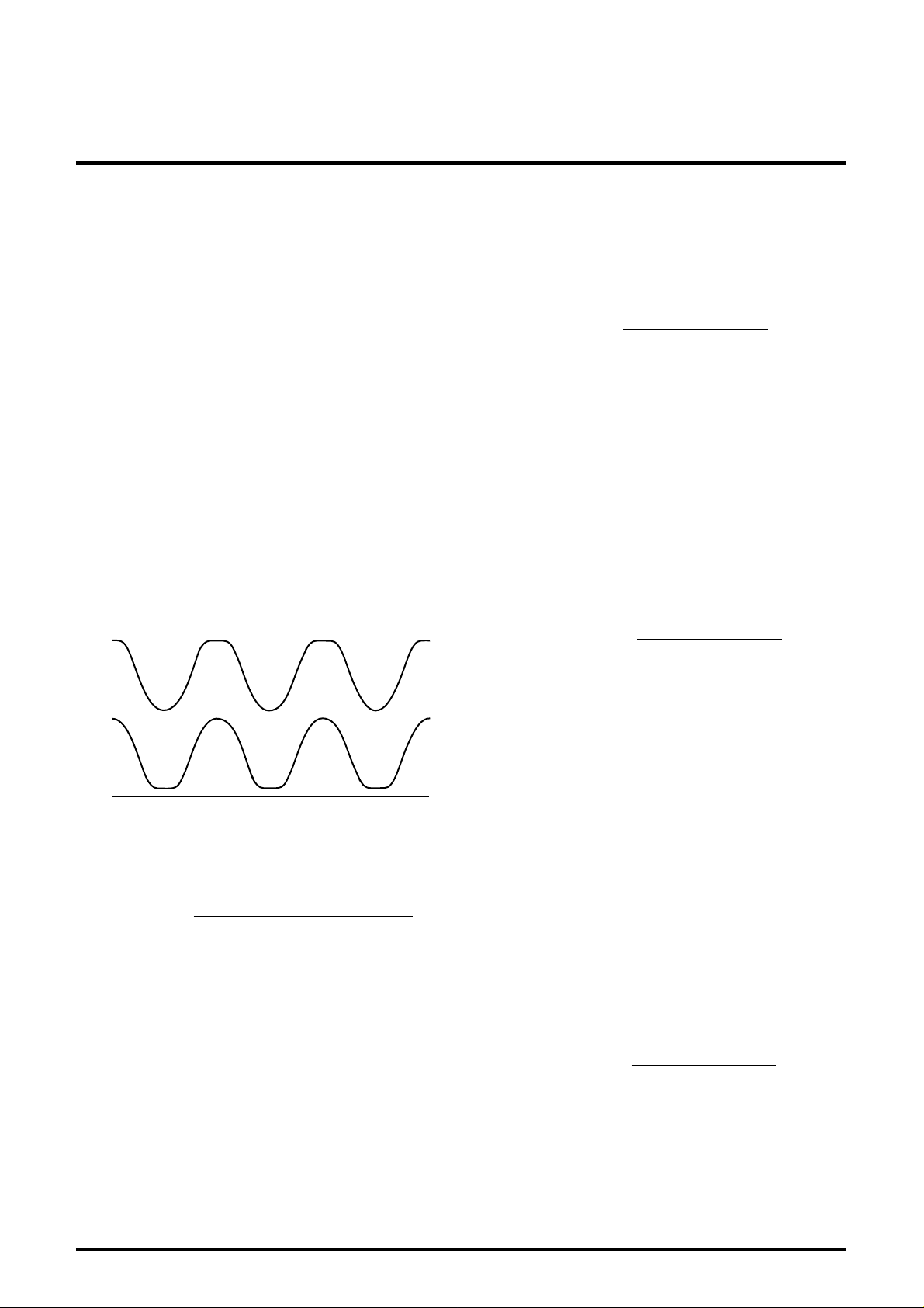
TYPICAL CHARACTERISTICS
THERMAL DERATING (MAXIMUM RATING)
1800
1600
1400
1200
1000
800
600
400
200
POWER DISSIPATION Pd (mW)
0 25 50 75 100 125
AMBIENT TEMPERATURE Ta (°C)
85
150-20
8
Page 9

APPLICATION EXAMPLE
110V
MITSUBISHI ICs (Monitor)
M52732SP
3-CHANNEL VIDEO AMPLIFICA TION
CRT
DC CLAMP
0 to 12V
0 to 12V
0 to 12V
1k
28
132
2627
1k 1k
25
24 2021 19 1718 16 15
NCNC
23
22
NC
M52732SP
4
6
598101211 13 14
7
0 to 12V
0 to 12V
12V CLAMP
INPUT
(B)
INPUT
(G)
INPUT
(R)
Units Resistance : Ω
9
Capacitance : F
Page 10

MITSUBISHI ICs (Monitor)
M52732SP
3-CHANNEL VIDEO AMPLIFICA TION
DESCRIPTION OF PIN
Pin No. Name DC voltage (V ) Peripheral circuit of pins Description of function
1
5
9
2
6
10
VCC (B-ch)
VCC (G-ch)
VCC (R-ch)
B-IN
G-IN
R-IN
12 −
1k
2.9
The voltage to be applied
to 3 channels shall be
equal.
VCC
24.7k
3.6k
GND
3
B SUB
CONTRAST
7
G SUB
CONTRAST
11
R SUB
CONTRAST
4, 25
8, 21
12, 17
GND (B-ch)
GND (G-ch)
GND (R-ch)
13 CONTRAST 6.9
4k
4.0
72k
GND −
4k
72k
0.12mA
0.4mA
Vcc
GND
Vcc
GND
14
CLAMP
PULSE
V
CC
50k
14
GND
10
Page 11

MITSUBISHI ICs (Monitor)
M52732SP
3-CHANNEL VIDEO AMPLIFICA TION
DESCRIPTION OF PIN (cont.)
Pin No. Name DC voltage (V ) Peripheral circuit of pins Description of function
VCC
30k
15 BRIGHT
15
GND
16 V
18
22
26
CC 12 −
NC
19
23
27
20
24
28
R HOLD
G HOLD
B HOLD
B OUT
G OUT
R OUT
Variable
Variable
Vcc
1k
GND
VCC
A resistor is needed at
the GND side. Choose
any resistance value
under 15mA according to
the driving capability
required.
50
11
 Loading...