

Page 1
MITSUBISHI ICs (Monitor)
M52721SP
WIDEBAND VIDEO PREAMPLIFIER WITH OSD MIX
DESCRIPTION
The M52721SP is a wideband video preamplifier with 200MHz
band.
FEATURES
•
Input:0.7V
•
Maximum gain:20dB
•
Frequency band:200MHz (-3dB)
•
Contrast control (0 to 5V
•
Brightness control (0 to 5V
•
Built-in OSD MIX circuit
P-P
(Typical), Output:7V
DC
DC
P-P
(Maximum)
)
)
APPLICATION
Display monitor
RECOMMENDED OPERATING CONDITION
Supply voltage range....................................................11.5 to 12.5V
Rated supply voltage................................................................12.0V
Operating temperature..............................................-20 ° C to +85 ° C
Circuit current...........................................................................60mA
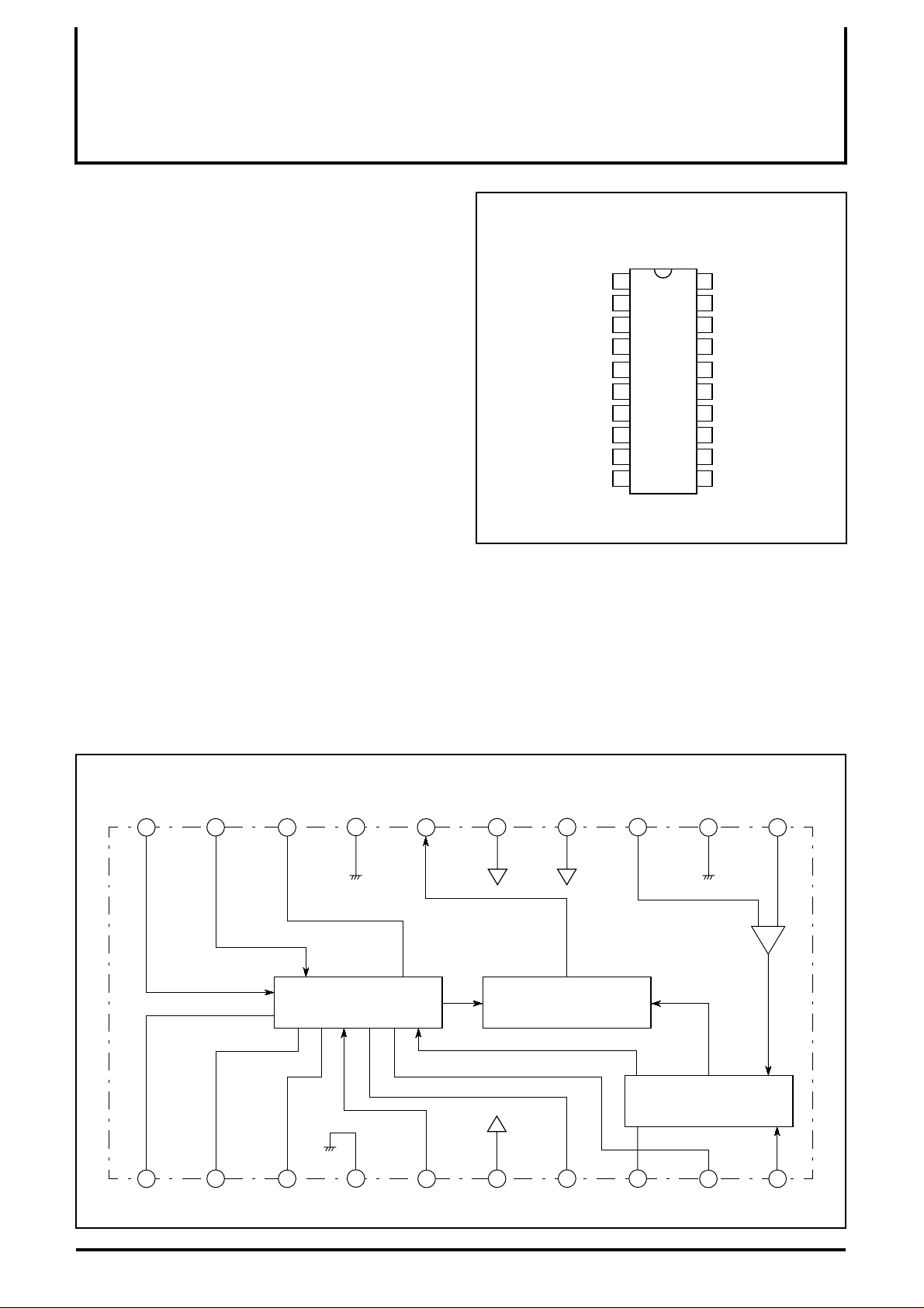
PIN CONFIGURATION (TOP VIEW)
CAP
REF.C
F.B.C
GND 1
VIDEO IN
V
CC1
CONTRAST
CLAMP HOLD
OSD.C
+
CLAMP
IN
1
2
3
4
7
8
20
19
18
M52721SP
17
165
156
14
13
129
1110
OSD BLK IN
OSD MIX IN
OSD ADJUST
GND 3
VIDEO OUT
V
VCC2
F/B
GND 2
F/B
Outline 20P4B
CC3
+
–
BLOCK DIAGRAM
OSD
BLK IN
20
1
OSD
MIX IN
OSD
ADJUST
19
2
18
3
17
CONTRAST
AMP
4
16
5
VCC3
15
6
V
CC2GND 3 VIDEO OUT F/B
BRIGHTNESS
AMP
CONTRASTGND 1 VCC1CAP
1314
87
HOLD
+
GND 2 F/B
12
CLAMP
9
11
–+
10
CLAMP
–
+
INCLAMP OSD.CVIDEO INF.B.CREF.C
1
Page 2
°
°
±
−
−
MITSUBISHI ICs (Monitor)
M52721SP
WIDEBAND VIDEO PREAMPLIFIER WITH OSD MIX
ABSOLUTE MAXIMUM RATINGS
(Ta=25 ° C, unless otherwise noted)
Symbol Parameter Ratings Unit
V
CC
P
d
T
opr
T
stg
V
opr
V
opr’
Surge Electrostatic discharge
ELECTRICAL CHARACTERISTICS
Supply voltage 13.0 V
Power dissipation 1524 mW
Operating temperature -20 to +85
Storage temperature -40 to +150
Recommended operating supply voltage 12.0 V
Recommended operating supply voltage range
11.5 to 12.5 V
200 V
(Ta=25 ° C, V
CC
=12V, unless otherwise noted)
Test conditions
External supply
SWA
Input
SW5
SG8
SG8
SG8
SG8
SG8
SG2
SG3
SG5
SG5
SG8
voltage (V)
V11
Bright-
ness
V18
OSD
Adj
V7
Con-
trast
a
5.0 0.5 0
a
2.5 0.5 0
a
5.0 2.0 0
a
2.5 2.0 0
a
1.0 2.0 0
a
2.5 open 0 c b b -1 0 3 dB
a
2.5 open 0 c b b -3 -2 3 dB
a
4 2.4 0
a
4 2.4 0
a
4 2.4 4
Symbol Parameter
I
V
V
CC
omax
imax
Circuit current A a b 5.0 3.0 5.0 c b b 40 52 64 mA
Output dynamic range T.P16 b
Maximum allowable input T.P16 b
Test
point
Gv Maximum gain T.P16 b
V
V
V
V
V
F
F
T
T
V
W
OT
OT
V
V
O
O
CR1
CR2
B1
B2
B3
1-a
2-a
r
f
10th
10
r
f
19th
20th
aj1
aj2
Contrast control
characteristics 1
Contrast control
characteristics 2
Brightness control
characteristics 1
Brightness control
characteristics 2
Brightness control
characteristics 3
Frequency
characteristics 1-a f=100MHz
Frequency
characteristics 2-a f=200MHz
Pulse characteristics
(rise time)
Pulse characteristics
(fall time)
T.P16 b
T.P16 b
T.P16 b b 5.0 1.0 0
T.P16 b b 5.0 2.0 0
T.P16 b b 5.0 3.0 0
T.P16 b
T.P16 b
T.P16 b
T.P16 b
Clamp pulse threshold voltage T.P16 b b 4 2.4 0
Clamp pulse minimum width T.P16 b b 4 2.4 0
OSD pulse characteristics
(rise time)
OSD pulse characteristics
(fall time)
T.P16 b b 4 2.4 4
T.P16 b b 4 2.4 4
OSD input threshold voltage T.P16 b b 4 2.4 4
BLK input threshold voltage T.P16 b
OSD adjust control
characteristics 1
OSD adjust control
characteristics 2
T.P16 b b 4 2.4 4
T.P16 b b 4 2.4 2
C
C
Pulse
SW19
SW10
OSD
Clamp
MIX
a
SG6
a
SG6
a
SG6
a
SG6
a
SG6
a
SG6
a
SG6
a
SG6
a
SG6
a
SG6
a
SG6
a
SG6
a
SG6aSG7
a
SG6aSG7
a
SG6aSG7
a
SG6
a
SG6aSG7
a
SG6aSG7
Limits
SW20
OSD
Min. Typ. Max.
Unit
BLK
b b 8.0 8.9 11.5 V
bb
−
0.7 1.0 V
b b 17.0 20.0 23.0 dB
b b 13.0 15.0 17.0 dB
b b 5.0 7.2 9.1 dB
b b 0.6 1.0 1.4 V
b b 1.6 2.0 2.4 V
b b 2.6 3.0 3.4 V
bb
bb
−
2.0 5.0 nsec
−
1.5 5.0 nsec
b b 1.9 2.0 5.0 V
b b 0.7 0.8
b
b
5.0 10.0 nsec
5.0 10.0 nsec
−µ
sec
b 2.2 2.3 5.0 V
a
b
2.8 2.9 5.0 V
SG7
b 5.9 6.3 6.8 V
b 2.9 3.3 3.7 V
P-P
P-P
DC
DC
DC
DC
DC
DC
P-P
P-P
2
Page 3
ELECTRICAL CHARACTERISTICS TEST METHOD
CC
I
Circuit current
When there is no signal, fix SWA on side “a”, and measure I
using ampere meter A.
omax
V
Output dynamic range
Input SG8 to pin 5, and set V11 at 0.5V
.
.
.
.
.
MITSUBISHI ICs (Monitor)
M52721SP
WIDEBAND VIDEO PREAMPLIFIER WITH OSD MIX
V
B2
Brightness control characteristics 2
Set brightness (V11) at 2.0V, and measure the output of TP16 with
,
a voltmeter. This value is V
CC
B3
V
Brightness control characteristics 3
Set brightness (V11) at 3.0V, and measure the output of TP16 with
a voltmeter. This value is V
B2
B3
(V)
9.0
0.0
TP16 OUTPUT WAVEFORM
Gradually increase the amplitude of SG8 from 700mV, and
measure the amplitude of the TP16 output waveform when the
upper side of the waveform becomes distorted.
V
Maximum allowable input
imax
From the condition in Vomax above, change V7 to 2.5V, gradually
increase the amplitude of SG8 from 700mV
P-P
, and read the input
signal amplitude when the output signal starts to be distorted.
Gv Maximum gain
Read the amplitude of TP16 output: it should be taken as V
is determined by:
V=20LOG
G
V
V0 [VP-P]
0.7 [V
P-P]
[dB]
The maximum gain G
0
.
1-a
F
Frequency characteristics 1-a
F
2-a
Frequency characteristics 2-a f=200MHz
f=100MHz
With zero resistance between pins 13 and 16, apply a DC voltage to
pin 5 so that the bottom of the input waveform reaches 2.6V. Next,
apply a DC voltage to pin 8 so that the bottom of the output
waveform reaches 2.4V.
Input SG1 and measure the amplitude of TP16 output (V
Input SG2 and measure the amplitude of TP16 output (V
Input SG3 and measure the amplitude of TP16 output (V
F
and F
1-a
T
r
Pulse characteristics (rise time)
T
f
Pulse characteristics (fall time)
1. Measure the rise time T
are determined by:
2-a
1-a=20LOG
F
2-a=20LOG
F
02 [VP-P]
V
V
01 [VP-P]
V
03 [VP-P]
V01 [VP-P]
and fall time T
r1
[dB]
[dB]
between 10 and 90%
f1
).
01
02
).
03
).
of the input pulse with an active probe.
2. Next, measure the rise time T
and fall time T
r2
between 10 and
f2
90% of the output pulse with an active probe.
2
r (nsec)= (Tr2)
T
Tf (nsec)= (Tf2)2-(Tf1)
-(Tr1)
2
2
CR1
V
Contrast control characteristics 1
Set V7 at 2.5V, and read the amplitude of TP16 output: it should be
taken as V
CR2
V
01
V
CR1=20LOG
V
01 [VP-P]
0.7 [V
P-P]
Contrast control characteristics 2
[dB]
Set V7 at 1.0V, and read the amplitude of TP16 output: it should be
taken as V
V
B1
02
02 [VP-P]
CR2=20LOG
V
V
0.7 [V
P-P]
[dB]
Brightness control characteristics 1
Set brightness (V11) at 1.0V, and measure the output of TP16 with
a voltmeter. This value is V
B1
3
V
Clamp pulse threshold voltage
10th
While monitoring the output (approx. 2.4V
DC
), decrease the SG6
pulse width gradually and measure the SG6 amplitude when the
output reaches 2.4V or more.
W
Clamp pulse minimum width
10
While monitoring the output (approx. 2.4V
), decrease the SG6
DC
amplitude gradually and measure the SG6 pulse width when the
output becomes 2.4V or more.
OT
OSD pulse characteristics (rise time)
r
OT
OSD pulse characteristics (fall time)
f
Measure the OSD rise time T
r
and OSD fall time T
f
between 10 and
90% of the output pulse with an active probe.
V
19th OSD input threshold voltage
While monitoring the output, decrease the SG7 amplitude gradually
and measure the SG7 amplitude when the output reaches 0V.
Page 4

MITSUBISHI ICs (Monitor)
M52721SP
WIDEBAND VIDEO PREAMPLIFIER WITH OSD MIX
V20th BLK input threshold voltage
Make sure that signal is not output in synchronization with SG7
O
Measure the amplitude of the output.
(blanking portion).
Next, while monitoring this output, decrease the SG7 amplitude
gradually and measure the SG7 amplitude when the blanking
portion disappears.
Oaj2 OSD adjust control characteristics 2
The conditions are the same as in O
at 2V.
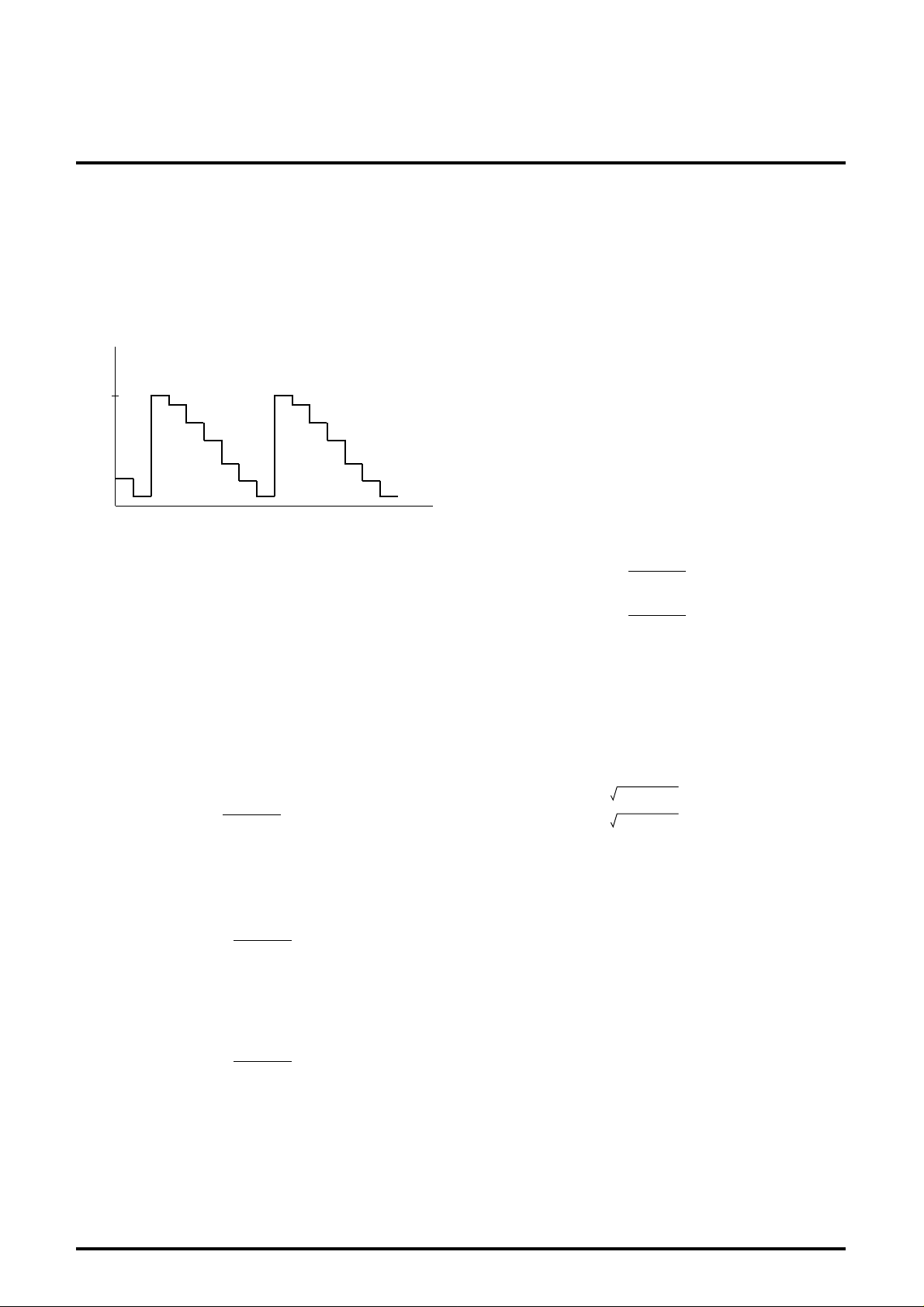
INPUT SIGNAL
SG No. Signals
Sine wave with amplitude 0.7VP-P (100kHz, amplitude partially variable∗)
SG1
SG2 Sine wave with amplitude 0.7V
SG3 Sine wave with amplitude 0.7VP-P (f=200MHz)
Pulse with amplitude 0.7VP-P (f=30kHz, duty=50%)
SG5
P-P (f=100MHz)
aj1 OSD adjust control characteristics 1
aj1 above except that V18 is set
0.7VP-P
0.7VP-P
SG6
+
CP
SG7
BLK,
OSD
signals
SG8
Standard
video
stepped
wave
Pulse with amplitude 4.0VP-P and pulse width 3.0µs synchronous with the pedestal part of standard video stepped wave
(f=30kHz, pulse width and amplitude partially variable)
4.0VP-P
0V
Pulse with amplitude 4.0V
3.0µs
P-P and pulse width 10µs synchronous with the image part of standard video stepped wave
(f=30kHz, amplitude partially variable∗)
4.0VP-P
0V
Video signal with pulse width 0.7V
10µs
P-P (f=30kHz, amplitude partially variable∗)
4
Page 5

TEST CIRCUIT
MITSUBISHI ICs (Monitor)
M52721SP
WIDEBAND VIDEO PREAMPLIFIER WITH OSD MIX
SG7
b
SW20
SG7
a
SW19
20
a
b
19
V18
18
OSD VCC3OSD OSD VCC2GND 3 VIDEO OUT
ADJUSTMIX INBLK IN
17
470
T.P16
16
2.2k
15
14
M52721SP
CONTRASTGND 1 VCC1CAP
1
1µ 10µ 10µ 2.2µ 1µ
2
3
0.01µ
SG1
SG2
SG3
SG5
SG8
54
SW5
6
b
7
V7
13
F/B
CLAMP
HOLD
8
BRIGHTNESS
V11
12
+
GND 2
OSD.CVIDEO INF.B.CREF.C
9
F/B
CLAMP
a
11
10
–
+
IN
SW10
b
ca
SG6
100µ0.01µ
A
b
a
SWA
TYPICAL CHARACTERISTICS
THERMAL DERATING (MAXIMUM RATING)
2000
1600
1524
1200
800
400
POWER DISSIPATION Pd (mW)
0 25 50 75 100 125
AMBIENT TEMPERATURE Ta (°C)
85
793
When
standard
substrate
is mounted
150-20
12V
Units Resistance : Ω
Capacitance : F
5
Page 6

APPLICATION EXAMPLE
1. External Feed Back
MITSUBISHI ICs (Monitor)
M52721SP
WIDEBAND VIDEO PREAMPLIFIER WITH OSD MIX
+B
5V
0V
OSD
BLK IN
20
1
CAP
OSD
MIX IN
5V
0V
1µ 10µ 10µ
0.01µ
19
2
OSD
ADJUST
N.P
1µ
OUTPUT
STAGE
Inverted
amplifier
470
BRIGHTNESS
0.01µ
GND 3
18
17
47µ
V
CC3
0.01µ
16
V
15
CC2
47µ
0.01µ
14
13
GND 2
12
CUT OFF ADJ
11
TO CRT
CC=12.0V
V
47µ 0.01µ
M52721SP
3
GND 1
VIDEO IN
F.B.CREF.C
3.3µ
30
R/G/B
54
IN
0.01µ
47µ
6
VCC1
0.01µ
CONTRAST
7
0 to 5V
8
CLAMP
HOLD
Green IN
Comp/H IN
V IN
9
OSD.C
2.2µ 0.1µ
M52036SP/M52346SP
M52347SP/M52347FP
10
CLAMP
Clamp Pulse
Sync Processor
+
IN
HD
VD
Units Resistance : Ω
Capacitance : F
6
Page 7

2. Internal Feed Back
MITSUBISHI ICs (Monitor)
M52721SP
WIDEBAND VIDEO PREAMPLIFIER WITH OSD MIX
+B
5V
0V
OSD
BLK IN
20
1
CAP
OSD
MIX IN
5V
0V
1µ 10µ 10µ
0.01µ
19
2
OSD
ADJUST
N.P
1µ
OUTPUT
STAGE
Inverted
amplifier
470
2.2k
GND 3
18
17
47µ
V
CC3
0.01µ
16
V
15
CC2
47µ
0.01µ
14
13
BRIGHTNESS
GND 2
12
CUT OFF ADJ
11
0.01µ
TO CRT
CC=12.0V
V
47µ 0.01µ
M52721SP
3
GND 1
VIDEO IN
F.B.CREF.C
3.3µ
30
R/G/B
54
IN
0.01µ
47µ
6
VCC1
0.01µ
CONTRAST
7
0 to 5V
8
CLAMP
HOLD
Green IN
Comp/H IN
V IN
9
OSD.C
2.2µ 0.1µ
M52036SP/M52346SP
M52347SP/M52347FP
10
CLAMP
Clamp Pulse
Sync Processor
+
IN
HD
VD
Units Resistance : Ω
Capacitance : F
7
Page 8

MITSUBISHI ICs (Monitor)
VCC
GND
0.2mA
2 or 3
M52721SP
WIDEBAND VIDEO PREAMPLIFIER WITH OSD MIX
DESCRIPTION OF PIN
Pin No. Name DC voltage (V ) Peripheral circuit of pins Description of function
VCC
38k
1
1 CAP 4.5
2
3
REF.C
F.B.C
4.5
Variable
6k
6k
GND
⋅Capacitance is required
between the pin and
GND.
⋅Capacitance is required
between the pin and
GND. If the output oscillates, consider the use
of additional non-polar
capacitance (approx. 1µ)
between pin 2 and pin 3.
4
12
17
GND1
GND2
GND3
GND −
5 VIDEO IN 2.6
6
14
V
CC1
VCC2
12
Impressed
7 CONTRAST Variable
2.6V
⋅Since pin 17 is a GND
pin for the output stage
only, make sure that it
does not interfere with
other GND pins.
VCC
3k
3k
⋅Clamped at about 2.6V
by the clamp pulse of pin
10.
5
CP
0.1mA
GND
−
15k
7
10k
GND
⋅Do not apply 5V or more
DC voltage.
8
Page 9

MITSUBISHI ICs (Monitor)
VCC
GND
53.9k
11 or 13
M52721SP
WIDEBAND VIDEO PREAMPLIFIER WITH OSD MIX
DESCRIPTION OF PIN (cont.)
Pin No. Name DC voltage (V ) Peripheral circuit of pins Description of function
8
CLAMP
HOLD
Variable
9 OSD.C −
10
CLAMP
+
IN
VCC
⋅Capacitance is required
between the pin and
GND.
The response is quicker
as the capacitance is
smaller, and as it is
larger, the response will
become more stable.
GND
8
VCC
1k 2k
18k
9
200 1k
GND
VCC
48.8k
Consequently, set this
capacitance according
to the signal contents.
⋅Capacitance is required
between the pin and
GND.
⋅Input a pulse of 1.9V or
more with pulse width
0.7µs or more.
−
10
1.9V or more
9
11
13
-
F/B
(BRIGHTNESS)
+
F/B
Variable
2.2V
GND
GND
⋅It is recommended that
the IC be used between
pedestal voltage 2V and
3V.
Page 10

MITSUBISHI ICs (Monitor)
M52721SP
WIDEBAND VIDEO PREAMPLIFIER WITH OSD MIX
DESCRIPTION OF PIN (cont.)
Pin No. Name DC voltage (V ) Peripheral circuit of pins Description of function
15 V
CC3
12V
Impressed
15
⋅Power supply for the
input stage only.
16 VIDEO OUT Variable
18
OSD
ADJUST
0 to 5V
Impressed
19 OSD MIX IN −
16
44
⋅A 370Ω or more resistor
is required across GND.
Make the resistor wiring
as short as possible.
GND
⋅Do not apply 5V or more
DC voltage.
When OSD MIX function
102k
VCC
108k
is not used, ground the
pin to GND.
18
75k
GND
80k
19
If external disturbing voltage intrudes into the pin,
which may affect IC output, consider the use of
an additional by-pass
capacitor as well.
VCC
⋅When not in use,
ground the pin to GND.
2.2 to 5V
GND
It is not possible to input
2.0V
2.4V
OSD MIX signal only. Be
sure to input the signal
with OSD BLK signal.
GND
20 OSD BLK IN −
2.8 to 5V
20
2.4V
⋅When not in use,
ground the pin to GND.
GND
Cannot be used for
0.5mA
GND
blanking of retrace line.
10
 Loading...