

Page 1
MITSUBISHI ICs (AV COMMON)
VCA
CTRL.
GEN.
CTRL.
CTRL.
CTRL.
4fsc
fsc
REF.
CLAMP
CLAMP
CLAMP
COMP.
DEV.
VCXO
DET.
ACC
SEPARATOR
S1S2S3
S1S2S3
MIX.
OUT
IN
IN
OUT
CONTROL
OUT
CONTROL 1
CONTROL 2
OUT
OUT
SWITH
OUT
GND
CAP.
IN 1
VCC2
VCC
IN 2
OUT
FILTER
IN
IN
IN
CAP.
OUT
FILTER
GND 2
A/D+
A/D-
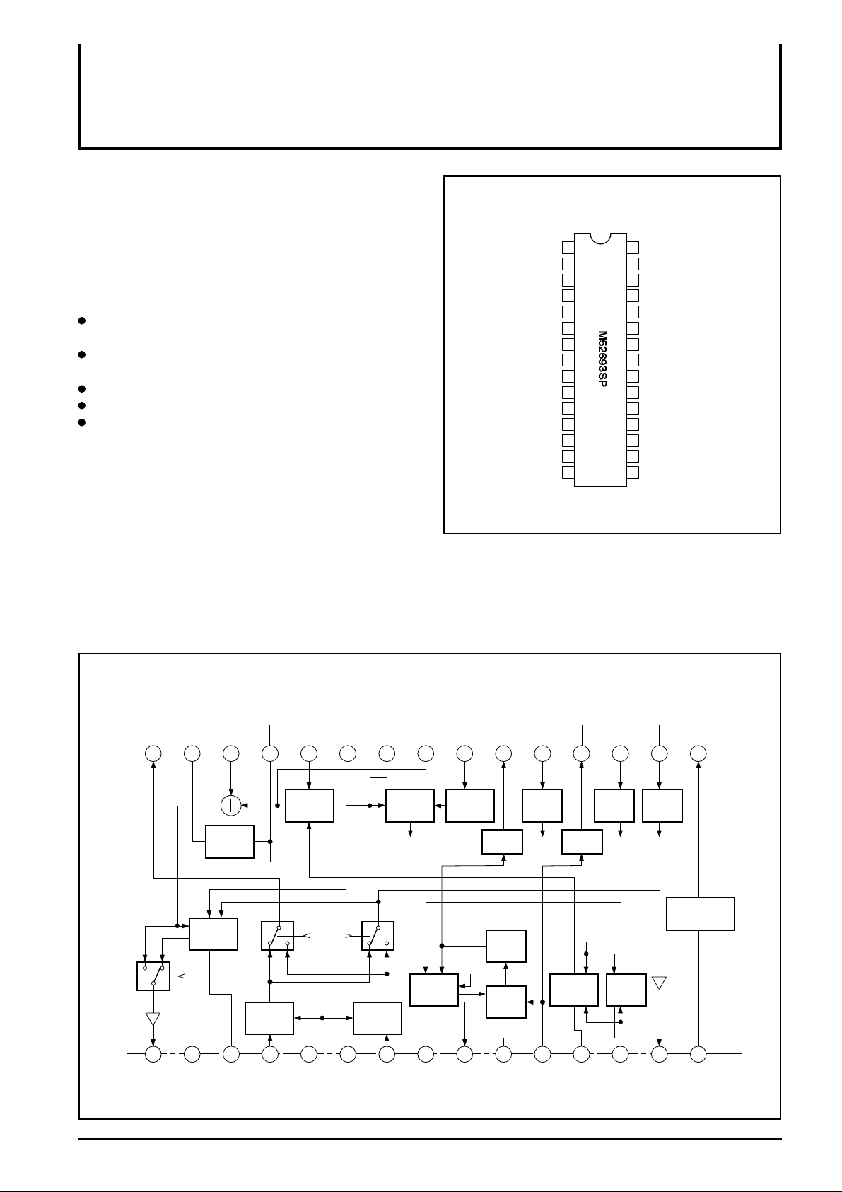
M52693SP
BURST LOCK CLOCK GENERATOR
DESCRIPTION
The M52693SP is a semiconductor integrated circuit developed for
analog signal processing of a picture-in-picture system, consisting
of a sync separator, an ACC, a burst lock clock generator circuit,
an analog switch and a clamp circuit, etc. It is also available on
digital video signal systems other than the above.
FEATURES
Low power dissipation of supply voltage 5.0V and circuit current
32mA (Typ.)
Built-in 4fsc burst lock clock generator circuit required for digital
video signal processing
Small picture chroma level following main picture burst level
Main picture pedestal level matching small picture pedestal level
Built-in reference voltage source for A/D converter
APPLICATION
TV, VCR
RECOMMENDED OPERATING CONDITION
Supply voltage range......................................................4.7 to 5.3V
Rated supply voltage.................................................................5.0V
PIN CONFIGURATION (TOP VIEW)
PIP CVBS OUT
GND
MAIN CLAMP CAP.
VIDEO IN 1
VCC2
VCC
VIDEO IN 2
APC FILTER
VCXO OUT
ACC FILTER
VCXO IN
VCA CAP.
MAIN CHROMA IN
MAIN VIDEO OUT
SYNC SEP. IN
1
2
3
4
5
6
7
8
9
10
11
12
13
14
15
Outline 30P4B
SUB CLAMP OUT
30
REFERENCE A/D+
29
SMALL LUMA IN
28
REFERENCE A/D-
27
SMALL CHROMA IN
26
25
GND 2
BURST GATE IN
24
VCA OUT
23
FREE RUN CONTROL
22
FSC OUT
21
INPUT SW CONTROL 1
20
4FSC OUT
19
INPUT SW CONTROL 2
18
SUPER SWITH
17
SYNC SEP. OUT
16
BLOCK DIAGRAM
REFERENCE
SUB
CLAMP
2
PIP
CVBS
MAIN
CLAMP
SMALL
LUMA
3
MAIN
REFERENCE
CHROMA
CHFOMA
4 81
VIDEO
SMALL
26
5
25
6
BURST
GATEINVCA
2428
BGP
bgp
VIDEO
APC
23
PHASE
FREE
RUN
22
FREE RUN
bgp
VCXO
FSC
21
1/4
1097
ACC
INPUT
SW
20
SW
11
VCXO
4FSC
INPUT
SW
19 17
1830 29 27
SW
bgp
LEVEL
121513
MAIN
VCA
CHROMA
SUPER
SW
14
MAIN
VIDEO
SYNC
SEP.
16
SYNC
SYNC
SEP.
Page 2

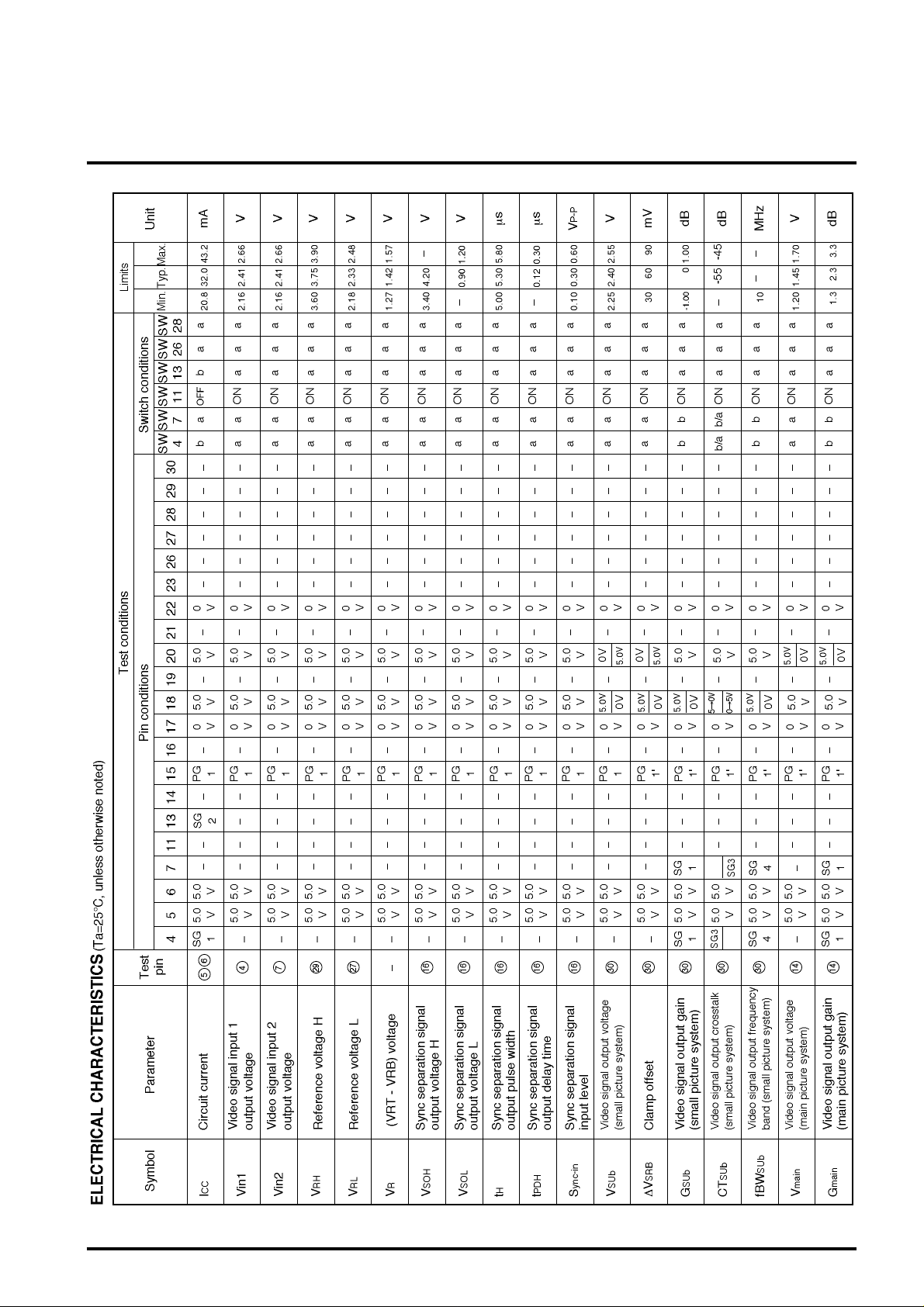
ABSOLUTE MAXIMUM RATINGS (Ta=25°C, unless otherwise noted)
Symbol Parameter Ratings Unit
VCC Supply voltage 6.0 V
Pd Power dissipation 1265 mW
Topr Operating temperature -20 to +75
Tstg Storage temperatare -40 to +125
MITSUBISHI ICs (AV COMMON)
M52693SP
BURST LOCK CLOCK GENERATOR
°C
°C
Page 3
MITSUBISHI ICs (AV COMMON)
M52693SP
BURST LOCK CLOCK GENERATOR
Page 4

MITSUBISHI ICs (AV COMMON)
M52693SP
BURST LOCK CLOCK GENERATOR
Page 5

MITSUBISHI ICs (AV COMMON)
M52693SP
BURST LOCK CLOCK GENERATOR
Page 6

(Pin 16 )
(PG 1 )
ELECTRICAL CHARACTERISTICS TEST METHOD
VSOH, VSOL, tH and tPDH
30181420151518182020141430303018301820201
VR
VR=VRH-VRL
SYNC IN
tPDH
MITSUBISHI ICs (AV COMMON)
M52693SP
BURST LOCK CLOCK GENERATOR
SYNC OUT
GND
tH
VSOH
Sync-in
Measure tH and tPDH when the input amplitude of pin is 0.1VP-P.
Make sure that tH and tPDH are within the allowable range. When
the input amplitude of pin is 0.6VP-P, make sure that tH and tPDH
are within the allowable range.
Vsub and ∆VSRB
Measure pin DC output voltage in correspondence to the "H"
and "L" states of pin .
CTsub, Cmain, and CTPIP
Measure crosstalk under the following input conditions:
CTsub
CTmain
CTPIP
Prameter
CTsub 1
Ctsub 2
CTmain 1
CTmain 2
CTPIP 1
CTPIP 2
Input signal
Sine wave
Amplitude
0.3VP-P
Frequency
3.58MHz
VSOL
If the voltage which appears at pin when pin is "H" is taken
as Vsub1, and the voltage which appears at pin when pin is
"L" is taken as Vsub2, the clamp offset is given by the following
expression:
DVSRB = (Vsub1 - V27), (Vsub2 - V27)
Gsub
Measure pin gain in correspondence to the "H" and "L" states of
pin .
Pin connection
Switching condition:Left
Input codition:Right
4 7
b
IN
a
- -
b
IN
a
- -
b
IN
a
- -
17
a
- -
b
IN
a
- -
b
IN
a
- -
b
IN
0V
0V
0V
0V
0 5V
0 5V
18
5 0V
0 5V
0V
0V
0V
0V
20
0V
0V
5 0V
0 5V
5V
0V
fBWsub
Measure pin frequency characteristics in correspondence to the
"H" and "L" states of pin . Condition: ≤-3dB
Vmain
Measure pin DC output voltage in correspondence to the "H"
and "L" states of pin .
Gmain
Measure pin gain in correspondence to the "H" and "L" states of
pin .
fBWmain
Measure pin frequency characteristics in correspondence to the
"H" and "L" states of pin . Condition: ≤-3dB
∆VPIP
If the voltage which appears at pin when pin is "H" is taken
as Vpip1, and the voltage which appears at pin 1 when pin is
"L" is taken as Vpip2, ∆VPIP is given by the following expression:
∆VPIP = Vpip1 - VPIP , Vpip2 - VPIP
Page 7

MITSUBISHI ICs (AV COMMON)
1
V4fSCL
191919
19
1919131313
12120120
23
Apply 5.0V to pin . Define as VOS1 the amplitude which appears
at pin a when pin is "H", and as VOM1 the amplitude which
appears when pin is "L". Then apply 0V to pin . Define as
VOS2 the amplitude which appears at pin when pin is "H",
and as VOM2 the amplitude which appears at pin when "L".
CTPIPS is given under the above conditions by the equation given
below.
CTPIPS=20log (VOMI/VOSI), 201log (VOM2/VOS2)
VCAtyp, VCAmax, VCAmin, Gmax, Lvca
20 log {(amplitude of pin 23)/SG5}
V4fSCH, L; VfSCH, L; 4fsc; fsc
Make sure that the input signal at pin is synchronous with the
output signal at pin .
120117171171920
13
V4fSCH
VfSCL
VfSCH
M52693SP
BURST LOCK CLOCK GENERATOR
GPIPSC
Pin = 2.185V V1 = Amplitude of pin V23 = Amplitude of pin
GPIPSC = 20 log (V1/V23)
GPIP
Measure pin gain in correspondence to the "H" and "L" states of
pin .
fBWPIP
Measure pin frequency characteristics in correspondence to the
"H" and "L" states of pin . Condition: ≤-3dB
fBWPIPS
Condition: ≤-3dB
4fSC
PIN
19
GND
CTPIPS
PIN
21
GND
fcp (+)
1) Raise the frequency of SG8 input signal so that the signal is
synchronous with pin output signal.
2) Lower the SG8 frequency.
3) Measure the SG8 frequency (f1) when the SG8 input signal is
synchronous with the pin output signal.
4) fcp(+) = f1 - fc (fc = 3.579545MHz)
fcp (-)
1) Lower the frequency of SG8 input signal so that the signal is
synchronous with pin output signal.
2) Raise the SG8 frequency.
3) Measure the SG8 frequency (f2) when the SG8 input signal is
synchronous with the pin output signal.
4) fcp(-) = f2 - fc (fc = 3.579545MHz)
fSC
C-IN
Make sure that the pin input signal is synchronous with the pin
output signal when the input amplitude of pin is 0.20VP-P.
Then make sure that the pin input signal is synchronous with the
pin output signal when the input amplitude is 0.01VP-P.
Page 8

− − −
− − −
− − −
VOL
− − −
INPUT SIGNAL
SG No.
SG1
SG2
Input signal
NTSC system composite video signal (1VP-P)
Sine wave
Frequency: 3.58MHz
Amplitude : 0.1VP-P
MITSUBISHI ICs (AV COMMON)
M52693SP
BURST LOCK CLOCK GENERATOR
Remarks
− − −
SG2'
SG2''
SG3
SG4
SG5
SG6
Sine wave
Frequency: 3.58MHz
Amplitude : 0.2VP-P
Sine wave
Frequency: 3.58MHz
Amplitude : 0.01VP-P
Sine wave
Frequency: 3.58MHz
Amplitude : 0.3VP-P
C-Sync + sine wave
C-Sync
Frequency: 15.734kHz
Amplitude : 0.285VP-P
Sine wave
Frequency: 1/10MHz
Amplitude : 0.715VP-P
Sine wave
Frequency: 3.58MHz
Amplitude : 0.2VP-P
Y signal
Amplitude : 0.715VP-P
− − −
SG7
SG8
PG1
PG1'
Sine wave
Frequency: 1/10MHz
Amplitude : 0.2VP-P
Sine wave
Frequency: Variable
Amplitude : 0.1VP-P
C-Sync
Frequency: 15.734kHz
Amplitude : 0.3VP-P
VOL=2.75V
C-Sync
Amplitude : 0.1VP-P
0.6VP-P
− − −
− − −
Page 9

°C)
TEST CIRCUIT
MITSUBISHI ICs (AV COMMON)
M52693SP
BURST LOCK CLOCK GENERATOR
SW11
SW28
SW26
M
b
a
b
a
10µ 75
10µ 75
M
22
M
20
M
18
17
M
10µ
M
10µ
BGP in
0.01µ
500
0.01µ
M
10µ75
10µ
M
5
6
10µ75
10µ
M
2.2µ
513300.01µ
10µ
a
SW4
b
a
SW7
b
0.01µ
1.5k
0.47µ
1M
10µ
1µ75
a
SW13
1µ
b
M
301
292
283
274
265
256
247
238
229
2110
2011
1912
1813
1714
Notes:
1. Capacitance values are in FARADS
2. Resistors are in OHMS
3. : VCC : GND
TYPICAL CHARACTERISTICS
THERMAL DERATING (MAXIMUM RATING)
1.4
1.2
1.0
0.8
0.6
0.4
0.2
0
-20
25 75 125
AMBIENT TEMPERATURE Ta (
1615
16020 60 100
1400 40 80 120
M
Units Resistance : Ω
Capacitance : F
 Loading...