

Page 1
MITSUBISHI ICs (TV)
)
r
M52335SP
NTSC SYSTEM SINGLE-CHIPCOLOR TV SIGNAL PROCESSOR
DESCRIPTION
The M52335SP is a semiconductor integrated circuit thatintegrates
NTSC system color TV signal processing functions into a single
chip. It contains video IF, sound IF, picture, color, on-screen
character display and deflection signal processing functions.
Combining the IC with a simple output stage using a tuner and
transistors provides rational NTSC system color TV set design.
FEATURES
Large-scale single-chip integration provides set rationalization,
high reliability and less power dissipation.
PLL
-employed full sync detector circuit is used as a video detecto
circuit to improve characteristics such as DG, DP, 920kHz beat
and cross color.
A quadrature detector circuit is used as a sound IF FM detector
to simplify external circuits and improve linearity.
Coilless AFT.
Horizontal oscillator is obtained by counting down from x32
horizontalfrequencyoscillator usinga ceramicoscillator,
requiring no adjustment of horizontal free run frequency.
Vertical oscillator is obtained by counting down double horizontal
frequencyoscillatorgenerated by horizontal count-down,
requiring no vertical sync adjustment. Using a 2-wind system
provides high noise resistance capability.
Double AFC is used as a horizontal circuit to reduce horizontal
jitter in a weak electric field and screen distortion caused by
luminance change.
Also, the sync detector circuit allows use as a detector signal as
for sound muting or automatic tuning.
Built-in black expansion circuit
Built-in Y-delay line circuit.
Built-in on-screen character display circuit.
DCvoltagecontrol isapplied to picturequality, contrast,
luminance, color saturation, tint and sound volume.
APPLICATION
NTSC system color TV set
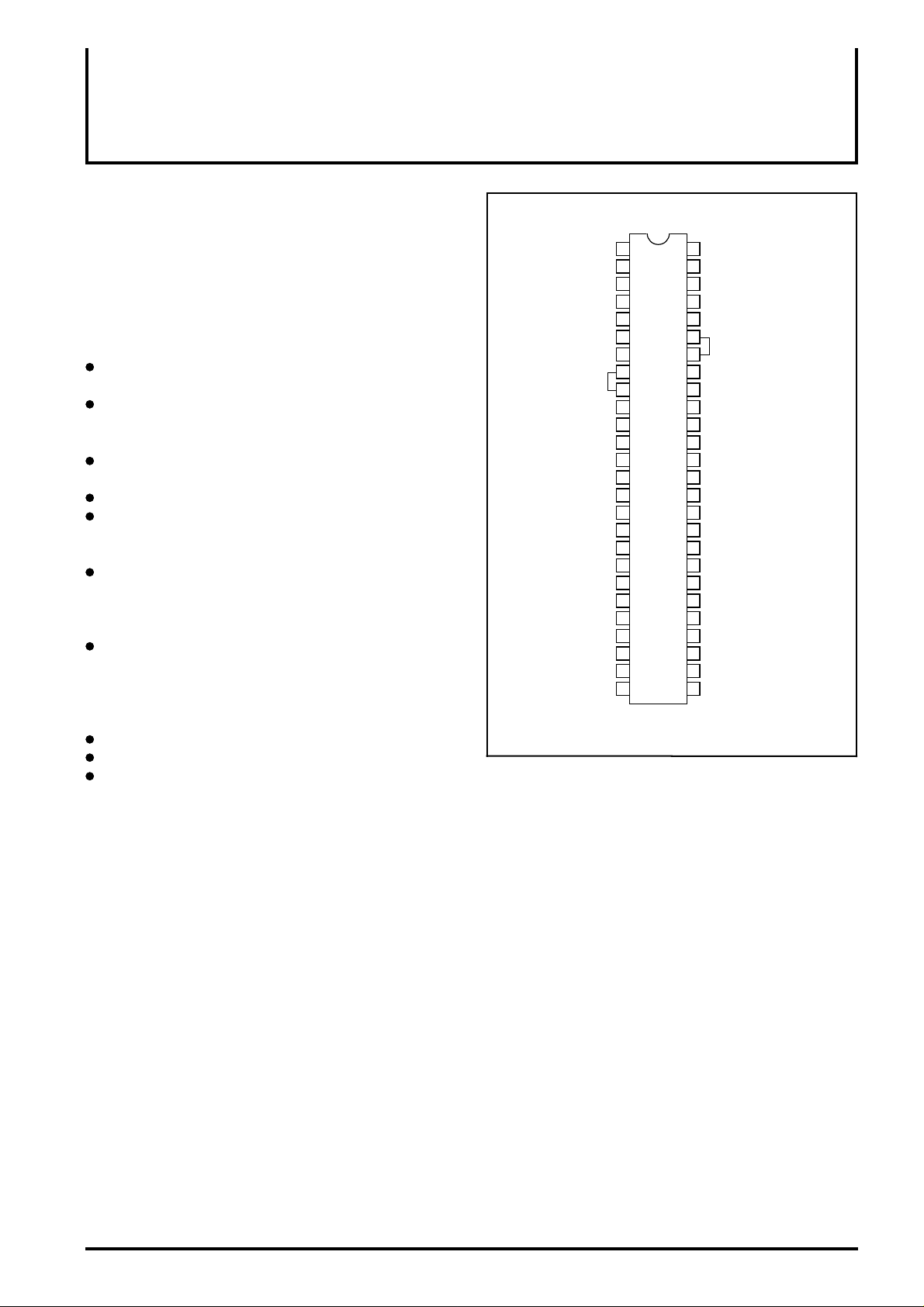
PIN CONFIGURATION(TOP VIEW
RF AGC OUT
EXT AUDIO IN
SOUND DET COIL
SOUND DET OUT
AF OUT
IF AGC FILTER
RF AGC DELAY ADJ.
GND-1 (VIF SIF)
VIF IN
CC-1 (VIF SIF)
V
APC FILTER
CC-2 (DEF)
V
AFC FILTER
AFC FBP IN
32f
H OSC.
X-RAY PROTECT
COINCIDENCE OUT
V. OUT
V
CC-2 (VC)
H. OUT
COLOR CONT.
-Y OUT
R-Y OUT
G-Y OUT
B-Y OUT
OSD B
1
2
3
4
5
6
7
8
9
10
11
12
13
14
15
16
17
18
19
20
21
22
23
24
25
26
52
VIDEO OUT
51
AFT OUT
50
AFT DEFEAT
49
SIF IN
48
47
VIDEO VCO COIL
46
TV IN
45
44
SYNC IN
Y SW OUT
43
EXT. VIDEO IN
42
M52335SP
41
Y IN
VIDEO TONE CONT.
40
PEDESTAL CLAMP
39
38
CHROMA IN/BRIGHT CONT.
37
GND-2 (VCJ)
36
CONTRAST CONT.
35
KILLER FILTER
BLACK HOLD
34
33
ACC FILTER
32
CHROMA OSC
APC FILTER
31
30
FAST BLK IN
TINT. CONT
29
28
OSD R
27
OSD G
Outline 52P4B
RECOMMENDED OPERATING CONDITION
Supply voltage........................................................................5V, 9V
Operating supply voltage..............................4.5 to 5.5V, 8.5 to 9.5V
Page 2
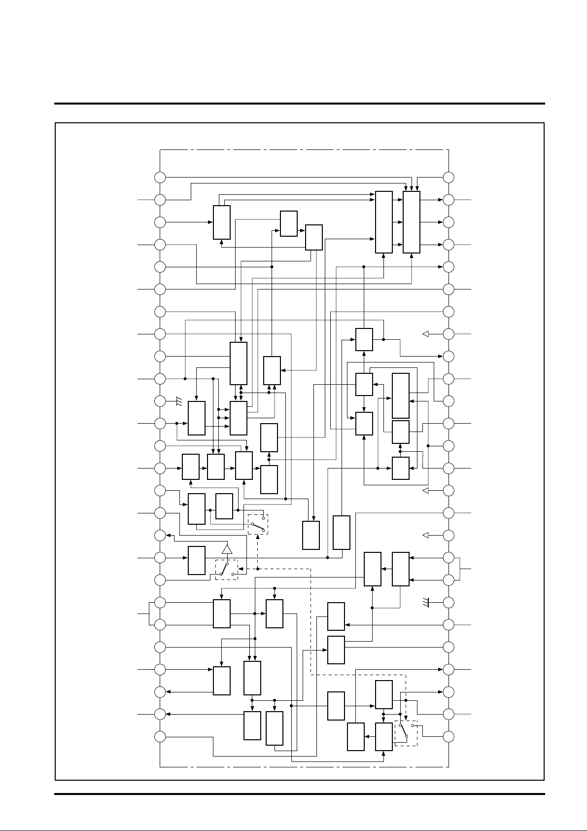
BLOCK DIAGRAM
MITSUBISHI ICs (TV)
M52335SP
NTSC SYSTEM SINGLE-CHIP COLOR TV SIGNAL PROCESSOR
OSD B
OSD R
TINT.
CONT. OSD G
FAST
BLK IN
APC
FILTER
OSC
CHROMA
ACC
FILTER
HOLD
BLACK
KILLER
FILTER
CONT.
CONTRAST
(VCD)
GND-2
CHROMA IN/
BRIGHT CONT.
CLAMP
PEDESTAL
CONT.
VIDEO TONE
EXT.
VIDEO IN
OUT Y IN
Y SW
B-Y OUT
29 272831
30
32
33
CHPOMA
40 39 37 36 3438 35
41
4250 49 47
43
TONE
VIDEO
BLACK
NTSC
AMP
RAST
CONT
STRECH
TINT
DET
ACC/KILLER
AMP
CHPOMA
BRIGHT
Y DL
APC
BLK
Y
DET
SEP
AMP
VCO
±45°
BCP
SEP
V SYNC
VCD
HCDAFC2
DEMO
COINCIDEN-
32fH
AFC
OSD
+9V
VC. VCC
CE DET
OSC
VCC
D. +9V
V/SIF
VCC +5V
G-Y OUT
23 24 26252221
-Y. OUT
20
H. OUT
18
V. OUT
17 19
X-RAY
15
14 16
AFC
13
12
VCC-2
1134 6
10
VCC-1
R-Y OUT
CONT.
COLOR
VCC-2(VC)
CE OUT
COINCIDEN-
PROTECT
H OSC.
32f
FBP IN
AFC
FILTER
(DEF)
APC
FILTER
(VIF SIF)
SYNC IN
VIDEO
VCO COIL
AFT
DEFEAT
OUT
VIDEO
RF
TV IN
AGC OUT AFT OUT SIF IN
SEP
SYNC
45
46 44
DET
VIDEO
EQ
AMP
APC
DET
LOCK
VCO
48
AFT
51
52
RF
IF
LIM
ACC
ACC
AF
AMP
VIF
AMP
FM
DET
ATT
VIF
AMP
VIF IN
8
79
GND-1
(VIF SIF)
RF AGC
IF AGC
FILTER
AF OUT
SOUND
DET OUT
SOUND
EXT
AUDIO IN
DELAY ADJ.
DET COIL
5
2
1
Page 3
MITSUBISHI ICs (TV)
M52335SP
NTSC SYSTEM SINGLE-CHIP COLOR TV SIGNAL PROCESSOR
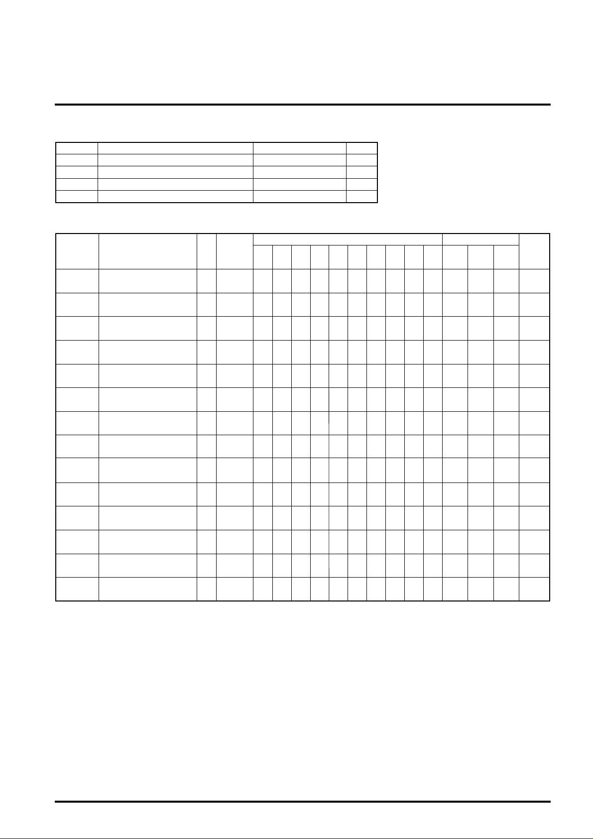
ABSOLUTE MAXIMUM RATINGS
Symbol Parameter Ratings Unit
VCC Supply voltage 5.0, 9.0 V
Pd Power dissipation 1.35 W
Topr Operating temperature
Tstg Storage temperatare -40 to 150
ELECTRICAL CHARACTERISTICS (Ta=25°C, unless otherwise noted)
Test
Symbol
ICC10 A10 ON ON 1 ON 24 33 42 mA
V51 51 ON ON ON ON 2 ON 3.0 3.3 3.7 V
Vo51 51 ON ON ON 2 ON 1.2 1.4 1.6 VP-P
V51L 51 ON ON ON 2 ON 1.5 1.75 1.95 V
Vin min. 51A ON ON ON 2 ON 48 55 dBµ
Vin max 51A ON ON ON 2 ON 101 107 dBµ
BW 51 ON ON ON 2 ON 5.0 6.5 MHz
IM 51 ON ON ON 2 ON 30 35 dB
S/N 51A ON ON ON 2 ON 49 55 dB
V50H 50 ON ON ON 1 ON 8.3 8.7 V
V50L 50 ON ON ON 1 ON 0.3 0.7 V
µAFT
V50D1 50 ON ON ON 1 ON 4.25 4.4 4.55 V
V50D2 50 ON ON ON 1 ON 4.25 4.4 4.55 V
Parameter
Circuit current
Video output DC voltage
Video detector output
signal voltage
Sync signal tip voltage
Input sensitivity
Maximum allowable input
Video frequency
characteristics
Inter-modulation
Video S/N
AFT output maximum
voltage
AFT output minimum
voltage
AFT sensitivity
AFT defeat voltage1
AFT defeat voltage2
Input
point
signal
A
SG. 1
A
SG. 2
A
SG. 3
A
SG. 4
A
SG. 10
A
SG. 11
A
SG. 2
A
SG. 6
A
SG. 7
A
50 ON ON ON 1 ON 55 75 95 mV/kHz
SG. 5
A
SG. 14
-20 to 65°C
CC VCC SSS
V
5
10 12 2 5 10
5.0 9.0
VV
5.0 9.0
VV
5.0 9.0
VV
5.0 9.0
VV
5.0 9.0
VV
5.0 9.0
VV
5.0 9.0
VV
Vari-
5.0 9.0
able
VV
5.0 9.0
VV
5.0 9.0
VV
5.0 9.0
VV
5.0 9.0
VV
5.0 9.0
VV
5.0 9.0
VV
°C
°C
Test conditions
SSS
S
12 49 52
10A
Limits
Min. Typ. Max.
Unit
Page 4
MITSUBISHI ICs (TV)
M52335SP
NTSC SYSTEM SINGLE-CHIP COLOR TV SIGNAL PROCESSOR
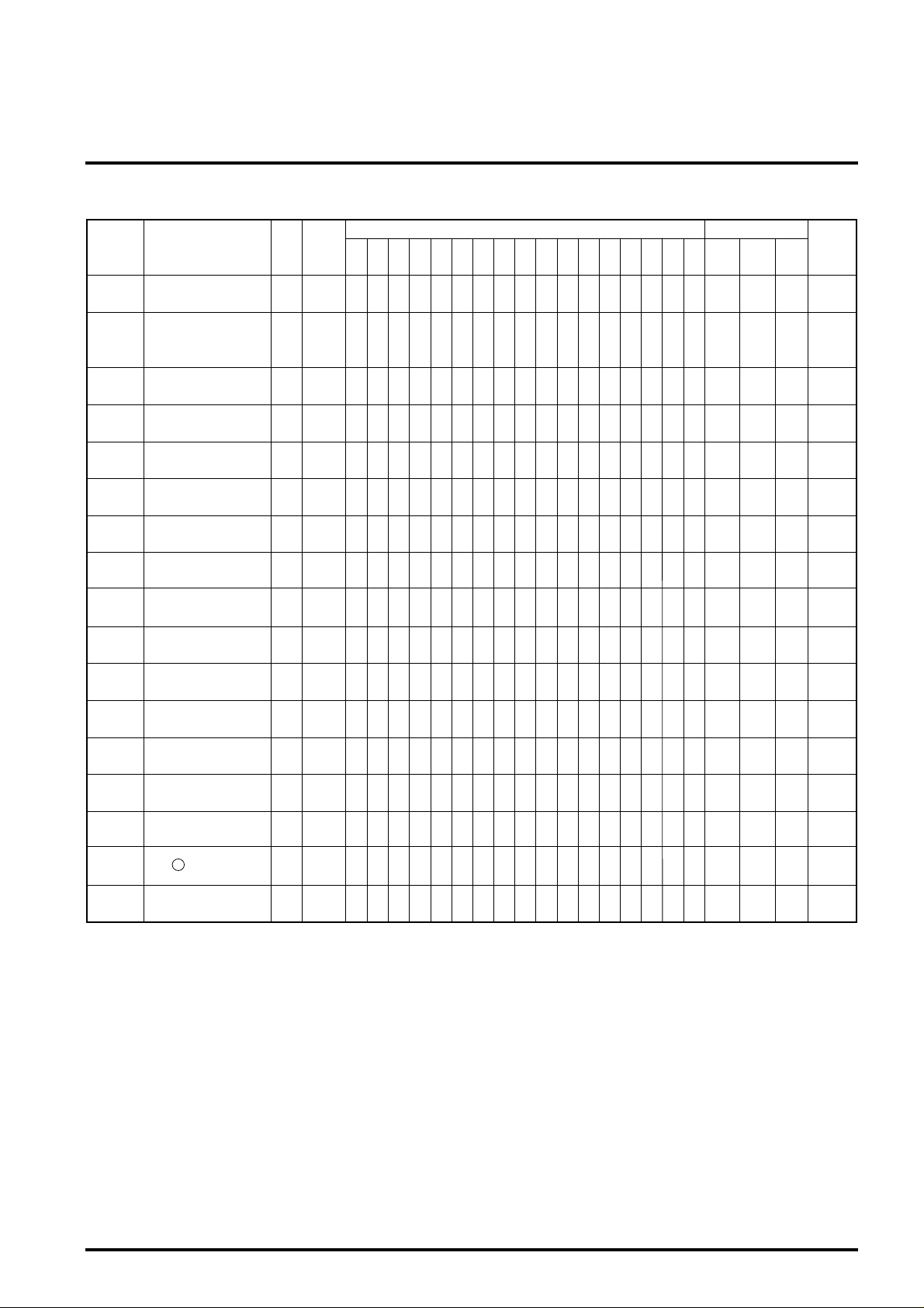
ELECTRICAL CHARACTERISTICS (cont.)
Test
Symbol
V50D3 50 ON ON ON 2 ON 4.25 4.4 4.55 V
V50M ON ON ON 1 ON 45 50 55
V52H 52 ON ON ON 2 ON 7.8 8.8 V
V52L 52 ON ON ON 2 ON 0.1 0.3 V
V3 3 ON ON ON ON 2 ON 2.65 3.15 3.65 V
V0AF 3 ON ON ON ON 2 ON 250 295 340 mVrms
LIM 3 ON ON ON ON 2 ON 49 55
AMR 3 ON ON ON ON 2 ON 44 55 dB
V04 4 ON ON ON ON 2 ON 250 295 340 mVrms
V40max 4 ON ON ON ON 2 ON 490 590 720 mVrms
ATT 4 ON ON ON ON 2 ON 70 75 dB
Parameter
AFT defeat voltage3
AFT mute input level
RF AGC maximum
voltage
RF AGC minimum
voltage
AF direct output DC
voltage
AF direct output signal
voltage
Limiting sensitivity
AMR
AF driver output
AF driver maximum
output
Maximum attenuation
point
A
50
Input
signal
A
SG. 1
A
SG. 1
variable
A
SG. 2
A
SG. 2
C
SG. 17
C
SG. 19
C
SG. 20
C
SG. 17
C
SG. 17
C
SG. 17
2
A 1012 2 5 10 1248 495152
VCC VCC SSSSSSSS
48
6
5.0 9.0
VV
5.0 9.0
VV
2.0 5.0 9.0
VVV
4.0 5.0 9.0
VVV
5.0 9.0
VV
5.0 9.0
VV
5.0 9.0
VV
5.0 9.0
VV
5.0 9.0
VV
9.0 5.0 9.0
VVV
1.0 5.0 9.0
VVV
Test conditions
S
S
2A
5A
10
S
A
48
S
A
Limits
Min. Typ. Max.
Unit
dBµ
dBµ
GAF 4 4.5 6.0 7.5 dB
S/N AF 4 ON ON ON ON 2 ON 60 66 dB
S TH 4 ON ON ON ON ON 2 ON 0.4 1.0 mVrms
THD AF 4 ON ON ON ON 2 ON 1.0 5.0 %
V48 48 ON ON ON ON 2 ON 3.8 4.4 5.0 V
V0EXT 4 ON ON ON ON 2 ON 580 710 830 mVrms
AF driver gain
Sound S/N
Sound switching
threshold voltage
AF driver maximum
output distortion
48
Pin voltage
Output signal voltage at
external input
C
SG. 21
C
1.1 9.0 5.0 9.0
SG. 17
A
SC. 17
B
SG. 23
9.0 5.0 9.0
VVV
VVVV
9.0 5.0 9.0
VVV
5.0 9.0
M
VV
0 4.5 5.0 9.0
VVVV
Page 5
MITSUBISHI ICs (TV)
M52335SP
NTSC SYSTEM SINGLE-CHIP COLOR TV SIGNAL PROCESSOR
ELECTRICAL CHARACTERISTICS (cont.)
Test
Symbol Parameter
V2 2 ON ON ON ON 2 ON 2.2 2.5 2.9 V
ISS ON ON ON 2 ON 1 0.05 0.1 0.2 mA
ICC12 A12 ON ON ON ON 2 1 29 34 39 mA
fH 20 ON ON ON ON ON ON 2 ON ON 1 15.4 15.800 16.2 kHz
V12 min.
fPHL ON ON ON ON ON ON 2 ON ON 1 -500 -600 Hz
fPHH ON ON ON ON ON ON 2 ON ON 1 +500 +600 Hz
V20H 20 ON ON ON ON ON ON 2 ON ON 1 3.0 3.65 4.65 V0-P
V20L 20 ON ON ON ON ON ON 2 ON ON 1 0 0.3 V0-P
TH 20 ON ON ON ON ON ON 2 ON ON 1212429
VRPO ON ON ON ON ON 2 ON ON 1 0.61 0.71 0.81 V
fV60 18 ON ON ON ON ON ON 2 ON ON 1 53.4 55 57.6 Hz
fPV60 18 ON ON ON ON ON ON 2 ON ON 1 64.9 67.5 70 Hz
V18H 18 ON ON ON ON ON ON 2 ON ON 1 7.0 8.0 9.0 V0-P
V18L 18 ON ON ON ON ON ON 2 ON ON 1 0.55 V0-P
TV60 18 ON ON ON ON ON ON 2 ON ON 1 494 544 594
V17H 17 ON ON ON ON ON ON 2 ON ON 1 7.7 8.5 V
V17L 17 ON ON ON ON ON ON 2 ON ON 1 0.33 0.5 V
ICC19 A19 ON ON ON ON ON 2 ON 38 48 58 mA
2
Pin voltage
Sync separation input
sensitivity current
H. V
CC inflow
Current
Horizontal free run
frequency
Horizontal oscillator
starting voltage
Horizontal pull-in
range 1
Horizontal pull-in
range 2
Horizontal output
maximum voltage
Horizontal output
minimum voltage
Horizontal output
pulse width
Overvoltage detector
operating voltage
Vertical free run
frequency 60
Vertical pull-in
frequency 60
Vertical output
maximum voltage
Vertical output
minimum voltage
Vertical output pulse
width
Coincidence output
maximum voltage
Coincidence output
minimum voltage
Circuit current
point
I
SS
20
12
20
E
20
E
20
16
20
Input
signal
ISS
f variable
D
SG. B
f variable
D
SG. B
D
SG. B
D
SG. B
D
SG. E
D SG. B
f variable
D
SG. A
D
SG. A
D
SG. A
D
SG. B
D SG. B
f=17kHz
VCC VCC VCC SSS SSS SSSSS SSS
36
101219 5 1012 131416 2022343544 4952 D
5.09.0
S
2
A
VV
9.0
V
9.0 9.0
VV
9.0
V
9.0
V
9.0
ON ON ON ON ON ON 2 ON ON 1 6.5 7.5 V
V
9.0
V
9.0
V
9.0
V
9.0
V
9.0
V
9.0
V
9.0
V
9.0
V
9.0
V
9.0
V
9.0
V
9.0
V
5.1 9.0 9.0
VVV
Test conditions
S
12
A
19
S
A
44
S
A
Limits
Min. Typ. Max.
Unit
µsec
µsec
Page 6
ELECTRICAL CHARATERISTIC (cont. )
Symbol
Ymax.
GY
GYmix.
GYmax.
VBRT
norm
VBRT
L
VBRT
H
GP
GT
norm
GT
min.
GT
max.
fBY
V40
VBLK
V
VBLK
TV
HBLK
H
YDL 1
YDL 2
Parameter
Maximum output
Standard gain
Contrast control
characteristic 1
Contrast control
characteristic 2
Brightness control
characteristic 1
Brightness control
characteristic 2
Brightness control
characteristic 3
Peaking value
Video tone control
characteristic 1
Video tone control
characteristic 2
Video tone control
characteristic 3
Frequency characteristic
40
Pin voltage
Vertical blanking voltage
Vertical blanking pulse
width
Horizontal blanking
theshold voltage
Y delay value 1
Y delay valye 2
Test
point
22 ON ON ON ON ON 2 5.4 6.4 VP-P
22 ON ON ON ON ON 2 7.0 11.0 15.0 dB
22 ON ON ON ON ON 2 -35 dB
22 ON ON ON ON ON 2 2.5 6.0 8.5 dB
22 ON ON ON ON ON 2 3.05 3.45 3.8 VP-P
22 ON ON ON ON ON 2 2.0 2.4 2.7 VP-P
22 ON ON ON ON ON 2 4.25 4.7 5.15 VP-P
22 ON ON ON ON ON 2 7.5 11.0 14.5 dB
22 ON ON ON ON ON 2 -1.2 -0.5 1.0 dB
22 ON ON ON ON ON 2 -4.8 -8.3 -11.8 dB
22 ON ON ON ON ON 2 1.2 4.2 7.2 dB
22 ON ON ON ON ON 2 5.0 8.0 MHz
40 ON ON ON ON ON 2 4.05 4.3 4.55 V
22 ON ON ON ON ON 2 6.9 7.1 V0-P
22 ON ON ON ON ON 2 1.31 1.38 1.44 msec
22
25A
0.2V
22
41
22
41
MITSUBISHI ICs (TV)
M52335SP
NTSC SYSTEM SINGLE-CHIP COLOR TV SIGNAL PROCESSOR
Input
signal
F
SG. F
F
SG. G
F
SG. G
F
SG. G
D
SG. A
D
SG. A
D
SG. A
F
SG. G
SG. J
F
SG. J
F
SG. J
F
SG. J
F
SG. K
E
SG. P
F
SG. T
F
SG. T
36 38 40
9.0 9.0 5.0 9.0 9.0
V VVVV
5.1 9.0 5.0 9.0 9.0
V VVVV
2.5 9.0 5.0 9.0 9.0
V VVVV
9.0 9.0 5.0 9.0 9.0
V VVVV
5.1 4.5 9.0 5.0 9.0 9.0
VVVVVV
5.1 2.5 9.0 5.0 9.0 9.0
VVVVVV
5.1 6.5 9.0 5.0 9.0 9.0
VVVVVV
5.1 5.0 9.0 9.0
V VVV
5.1 4.5 5.0 9.0 9.0
V VVVV
5.1 0 5.0 9.0 9.0
V VVVV
5.1 9.0 5.0 9.0 9.0
V VVVV
5.1 5.0 9.0 9.0
V VVV
5.1 5.0 9.0 9.0
V VVV
2.5 9.0 5.0 9.0 9.0
V VVVV
2.5 9.0 5.0 9.0 9.0
V VVVV
2.5 9.0 5.0 9.0 9.0
V VVVV
P-P
5.1 5.0 9.0 9.0
V VVV
5.1 0 5.0 9.0 9.0
VV VVV
VCC VCC VCC SSSSSSS
M
2A
–
Test conditions
10 12 19 10 12 19 20 22 34 35
ON ON ON ON ON 2 ON 6.9 7.1 V0-P
ON ON ON ON ON 2 225 260 295 nsec
ON ON ON ON ON 2 120 140 160 nsec
Limits
Min. Typ. Max.
Unit
Page 7
NTSC SYSTEM SINGLE-CHIP COLOR TV SIGNAL PROCESSOR
ELECTRICAL CHARACTERISTICS (cont. )
Test
Symbol Parameter
BS1
AVTH
AVTV
Black stretch
threshold 1
AV SW switching
threshold voltage
AV SW TV output signal
voltage
Input
point
signal
F
SG. U
22 ON ON ON ON ON 37 50 63 IRE
variable
H
43
2A
SG. G
H
SG. F
43 ON ON ON 2 1.4 1.5 1.6 VP-P
-6dB
2
21 36 40
A
5.1 5.0 9.0 9.0
V VVV
2.1
5.1 5.0 9.0 9.0
↓
1.0
V VVV
V
5.1 5.0 9.0 9.0
–
V VVV
MITSUBISHI ICs (TV)
Test conditions
VCC VCC VCC SSSSSS
10 12 19 10 12 19 20 22 34
1
↓
2
ON ON ON 2 1.0 1.5 2.1 V
M52335SP
Limits
Min. Typ. Max.
Unit
AVEXT
Cmax.
ACC-1
ACC-2
Vik
Vok
Cnorm.
Csmin.
Csmax.
Cumin.
AV SW EXT output signal
voltage
Chroma maximum output
ACC characteristic 1
ACC characteristic 2
Killer operation level
Killer color residual
Chroma standard output
Color control characteristic 1
Color control characteristic 2
Color tracking
characteristic 1
G
SG. F
43 ON ON ON 2 1.4 1.5 1.6 VP-P
-6dB
E
SG. L
25A ON ON ON ON 2 3.2 4.7 6.2 VP-P
0dB
E
SG. L
25A ON ON ON ON 2 -5.0 -1.0 0 dB
-20dB
E
SG. L
25A ON ON ON ON 2 -3.0 0 +3.0 dB
+6dB
E
G
SG. L
25A
variable
E
SG. Q
25A ON ON ON ON 2 15 35 mVP-P
0dB
E
SG. L
25A ON ON ON ON 2 1.0 1.45 1.85 VP-P
0dB
E
SG. L
25A ON ON ON ON 2 -40 -30 dB
0dB
25A ON ON ON ON 2 3.8 7.3 10.8 dB
25A ON ON ON ON 2 -48 -38 -30 dB
E
SG. L
0dB
E
SG. L
0dB
5.1 5.0 9.0 9.0
1.1
V VVV
V
6.5 9.0 9.0 5.0 9.0 9.0
VVVVVV
5.1 9.0 5.0 9.0 9.0
VVVVV
5.1 9.0 5.0 9.0 9.0
VVVVV
5.1 9.0 5.0 9.0 9.0
VVVVV
9.0 9.0 5.0 9.0 9.0
VVVVV
5.1 9.0 5.0 9.0 9.0
VVVVV
0 5.1 9.0 5.0 9.0 9.0
VVVVVV
9.0 5.1 9.0 5.0 9.0 9.0
VVVVVV
2.5 9.0 5.0 9.0 9.0
VVVVV
ON ON ON ON 2 -48 -41 -35 dB
–
Cumax.
Color tracking
characteristic 2
E
SG. L
25A ON ON ON ON 2 1.7 5.2 8.7 dB
0dB
9.0 9.0 5.0 9.0 9.0
VVVVV
Page 8
NTSC SYSTEM SINGLE-CHIP COLOR TV SIGNAL PROCESSOR
ELECTRICAL CHARACTERISTICS (cont. )
Test
Symbol
fPCL
Parameter
APC pull-in range 1
point
25A
G
Input
signal
F
SG. M
0dB
21 36 40
VCC VCC VCC SSSSSSS
10 12 19 10 12 19 22 34 36 39
5.1 9.0 5.0 9.0 9.0
VVVVV
MITSUBISHI ICs (TV)
M52335SP
Test conditions
ON ON ON ON 2 -0.3 -0.7 kHz
Limits
Min. Typ. Max.
Unit
fPCH
fPC
V23
V24
V25
V23-24
V24-25
V25-23
CL
B-Y
CL
R-Y
APC pull-in range 2
Total APC pull-in range
Modulated output DC
voltage 1
Modulated output DC
voltage 2
Modulated output DC
voltage 3
Modulated output DC
offset voltage 1
Modulated output DC
offset voltage 2
Modulated output DC
offset voltage 3
Modulated output
carrier leak 1
Modulated output
carrier leak 2
25A
23A ON ONON ON 2 ON 5.0 5.4 5.8 V
24A ON ONON ON 2 ON 5.0 5.4 5.8 V
25A ON ONON ON 2 ON 5.0 5.4 5.8 V
E
SG. M
G
0dB
E
SG. L
25 ON ON ON ON 2 0.2 VP-P
0dB
E
SG. L
23 ON ON ON ON 2 0.2 VP-P
0dB
5.1 9.0 5.0 9.0 9.0
VVVVV
5.1 9.0 5.0 9.0 9.0
VVVVV
5.1 9.0 5.0 9.0 9.0
VVVVV
5.1 9.0 5.0 9.0 9.0
VVVVV
4.5 5.1 9.0 5.0 9.0 9.0
VVVVVV
4.5 5.1 9.0 5.0 9.0 9.0
VVVVVV
ON ON ON ON 2 +0.3 +0.7 kHz
0.6 1.4 kHz
-0.3 0 +0.3 V
-0.3 0 +0.3 V
-0.3 0 +0.3 V
CL
G-Y
V21
SS
Y
SS
C
Modulated output
carrier leak 3
21
Pin voltage 1
Servise switch operation 1
Servise switch operation 2
E
4.5 5.1 9.0 5.0 9.0 9.0
SG. L
24 ON ON ON ON 2 0.2 VP-P
SG. L
21 ON ON ON ON 2 4.2 4.6 5.0 V
22 ON ON ON ON 2 10 90 mVP-P
SG. G
SG. L
25A ON ONON ON 2 10 90 mVP-P
VVVVVV
0dB
E
0dB
F
E
0dB
5.1 9.0 5.0 9.0 9.0
M
VVVVV
5.1 9.0 5.0 9.0 9.0
VVVVV
5.1 9.0 5.0 9.0 9.0
VVVVV
Page 9
NTSC SYSTEM SINGLE-CHIP COLOR TV SIGNAL PROCESSOR
ELECTRICAL CHARACTERISTICS (cont. )
Test
Symbol
Parameter
point
Input
signal
29 30 36 40
MITSUBISHI ICs (TV)
Test signal
VCC VCC VCC SSSSSSSSS
10 12 19 10 12 19 22 26 27 34 35 36
M52335SP
Limits
Min. Typ. Max.
Unit
SS
V
R-Y
-N
B-Y
G-Y
-N
B-Y
∠R-Y-N
∠G-Y-N
T min.
T max.
OSR
OSG
Service switch operation 3
NTSC demodulated
ratio 1
NTSC demodulated
ratio 2
NTSC demodulated
phase angle 1
NTSC demodulated
phase angle 2
TINT control
characteristics 1
TINT control
characteristics 2
On-screen threshold
voltage 1
On-screen threshold
voltage 2
18 ON ON ON ON 2 ON 8.1 9.0 V0-P
E
23A
SG. L
25A
0dB
E
24A
SG. L
25A
0dB
E
23A
SG. S
25A
0dB
E
24A
SG. S
25A
0dB
E
23A
SG. M
25A
0dB
E
23A
SG. M
25A
0dB
23A ON ON ON ON ON ON 2 ON 7.0 7.5 V
24A ON ON ON ON ON ON 2 ON 7.0 7.5 V
5.1 9.0 5.0 9.0 9.0
VVVVV
2.0 5.1 9.0 5.0 9.0 9.0
V VVVVV
2.0 5.1 9.0 5.0 9.0 9.0
V VVVVV
2.0 5.1 9.0 5.0 9.0 9.0
V VVVVV
2.0 5.1 9.0 5.0 9.0 9.0
V VVVVV
2.5 5.1 9.0 5.0 9.0 9.0
V VVVVV
6.5 5.1 9.0 5.0 9.0 9.0
V VVVVV
3.0 5.1 9.0 5.0 9.0 9.0
VVVVVV
3.0 5.1 9.0 5.0 9.0 9.0
VVVVVV
ON ON ON ON 2 ON 0.83 0.9 0.97
ON ON ON ON 2 ON 0.24 0.3 0.35
ON ON ON ON 2 ON 104 deg
ON ON ON ON 2 ON 241 deg
ON ON ON ON 2 ON +25 +45 +65 deg
ON ON ON ON 2 ON -65 -45 -25 deg
OSB
On-screen threshold
voltage 3
25A ON ON ON ON ON ON 2 ON 7.0 7.5 V
3.0 5.1 9.0 5.0 9.0 9.0
VVVVVV
Page 10

MITSUBISHI ICs (TV)
M52335SP
NTSC SYSTEM SINGLE-CHIP COLOR TV SIGNAL PROCESSOR
ELECTRICAL CHARACTERISTICS TEST
METHODS
V51
Measure the voltage at output in the no input state.
51
VO51
1. Enter SG 1 at 90dBµ.
2. Measure the amplitude at output .
51
Vin min.
1. Lower the SG 3 level. Represent Vin as an input level at which it
is 3dB lower than the Vo51 measured value.
Vin max.
1. Enter SG 4 at 90dBµ.
2. Define the output level as VA.
51A
3. Raise the SG 4 level. Represent Vin as an input level at which
the output level is 3dB lower than VA.
Vin max. = 20 log
51A
measured value
VA
(dB)
BW
1. Enter SG 10. Adjust f2 so that a 1MHz beat component can
appear at output .
2. Raise the f2 frequency. Measure a frequency which is -3dB
lower than the 1MHz component.
BW = (frequency of -3dB) - 58.75MHz (MHz)
IM
1. Enter SG 11. Apply voltage so that output is as shown in
the figure.
2. Calculate level difference between 920kHz and 3.58MHz at
51
output .
IM = 20 log
51
5
920kHz component
3.58MHz component
51
(dB)
V50H,V50L, µAFT
V50H, V50L and µAFT are shown below.
V
50H
50
Pin
5.5V
3.5V
57.75MHz 58.75MHz 59.25MHz
Standard µAFT = (mV/kHz)
(5.5-3.5) x 10
∆fkHz
∆f
V50L
f
3
V50D1,V50D2,V50D3
Use no signal, fo-2.5MHz, fo+1MHz and defeat SW to confirm that
output goes to 4.4V.
50
V50M
1. Enter SG 1. Lower the input level from 80dBµ.
2. Represent V50M as an input level at which voltage of output is
50
center (4.4V).
V52H
1. Enter SG 11. Apply 2.0V to .
2. Measure voltage .
52
6
V52L
1. Enter SG 10. Apply 4.0V to .
2. Measure voltage .
52
6
LIM
Decrease the SG 19 level. At test point 3, measure an input level
when a 400Hz component goes down 3dB lower than parameter
S2. AF direct signal voltage VOAF.
51
OUT
1.75V
S/N
1. Enter SG 2. Measure a rms value of output signal.
51
2. Standard
51 measured value (VP-P) x 10
S/N = 20 log
Vo
measured value (m Vrms)
3
x 0.7
(dB)
AMR
At test point 3, measure a 400Hz component and define it as Vam.
Standard value
AMR = 20 log (dB)
ATT
1. Measure a 400Hz component at output .
2. Standard value
ATT = 20 log (dB)
VOAF (m Vrms)
Vam (mVrms)
4
Vo4 max.
measured value
Page 11

MITSUBISHI ICs (TV)
M52335SP
NTSC SYSTEM SINGLE-CHIP COLOR TV SIGNAL PROCESSOR
GAF
4 max.
ATT = 20 log (dB)
Vo
measured value
S/N AF
1. Measure noise within the range of 20Hz to 100kHz at output .
2.
S/N AF = 20 log
STH
Enter SG 17. Measure output when AV SW is set to EXT
Vo4 max.
measured value (dB)
4
(2A=1.1V).
4
Iss
Increase the current of constant current source Iss. Measure a
current value of Iss when the horizontal frequency at output is
20
pulled in from free run.
V12 min.
Increase voltage from about 3V. Measure voltage applied
when horizontal oscillator waveforms begin to appear at (about
12
12
20
15kHz).
fPHL, fPHH
1. Lower the frequency of input signal SG B to make the input
waveform asynchronous to output waveform at pin .
20
2. Raise the input frequency. Measure the frequency at the
moment when the input waveform begin to synchronize with
output waveform . Define the frequency as lower pull-in
20
frequency fPHL.
3. Measure upper pull-in frequency fPHH in the same manner.
4. Represent the difference from reference value of 15.734kHz.
V20H,V20L,TH
V20H, V20L and TH are shown below.
TPRO
Raise the voltage applied to gradually. Represent TPRO as the
voltage at which output waveform at pin is as shown below.
Make sure that the voltage applied to is opened and retained.
16
20
GND
At VPRONormal
16
Y max.
Enter SG F. Measure the amplitude of output .
22
GY
1. Enter SG G. Measure the amplitude of output .
2. GY = 20 log (dB)
measured value mV
200mVP-P
P-P
22
GY min., GY max.
1. Enter SG G. Measure the amplitude of output . Define the
amplitude as VA or VB.
2. GY min. = 20 log (dB)
GY max. = 20 log (dB)
GY measured value (mVP-P)
GY measured value (mVP-P)
VA (mVP-P)
V
B (mVP-P)
22
VBRT norm,VBRT L,VBRT H
Enter SG A. Measure the level given below.
2Vo-p
Output waveform at pin
V20H
TH
V20L
20
GND
VBRT norm, VBRT L, VBRT H
GND
Gp
1. Define as VA the output signal voltage at the entry of SG G,
as VB the voltage at the entry of SG J.
V
2. G
P = 20 log (dB).
A
VB
22
Page 12

MITSUBISHI ICs (TV)
M52335SP
NTSC SYSTEM SINGLE-CHIP COLOR TV SIGNAL PROCESSOR
GT norm., GT min., GT max.
1. Change the applied voltage to 4.5V, 6.5V and 2.5V. Define
output signal measured values as VA, VB and VC,
22
40
respectively.
2. GT min. = 20 log (dB), GT max. = 20 log (dB)
VB
VA
VC
VA
GT norm. (dB) is represented by a change of VB (dB) at parameter
Y9 GP measurement.
fB [Y]
Measure the SG K frequency which is 3dB lower than the VA value
at parameter Y9 GP measurement.
VBLK V,VBLK TV
VBLK V and VBLK TV are shown below.
VBLK V
TBLK TV
GND
VBLK H
Raise the applied voltage 22A gradually. Represent VBLK H as a
voltage level at which output signal 25A disappears.
22
AVTH
1. Enter SG G into H input.
2. Apply voltage of 2.0V to 2A. Measure the amplitude of output
waveform at pin .
3. Apply voltage of 1.1V to 2A. If the output at pin becomes DC,
43
43
everything will be O.K.
AVTV,AVEXT
Enter SG F (-6dB) into inputs H and G. Measure the amplitudes of
output waveform at pin when the voltage applied to
43 2A
becomes OPEN and goes to 1.1V.
ACC-1,ACC-2
1. Define output signal voltages as VA,VB and VC,
respectively, when changing the SG L input level to 0, -20 and
+6dB.
ACC-1 = 20 log (dB)
2.
ACC-2 = 20 log (dB)
VB
VA
VC
VA
25A
Vik
Lower the SG L input level. Represent Vik as an input level when
output signal disappears.
25A
YDL 1, YDL 2
Enter SG T into . Measure the delay time of output waveform at
22
pin to the entry.
A
F
50IRE
50IRE
F Input Waveform
BA
YDL
B
OutputWaveform
at oin
F Input Waveform
Output Waveform
at pin
Represent by (nsec)
50IRE
50IRE
22
22
A B
Black stretch threshold
1. Set SG U at 200kHz, V1=0.35V and V2=0.1V. Enter them from
F. Define the range from the pedestal to the white peak as 100
IRE.
2. Lower V2 from about 75 IRE gradually. Measure an operating
point which causes black expansion.
Vok
Enter SG Q. Measure output signal voltage .
25A
Cnorm.
Enter SG L. Measure output signal voltage when the voltage
applied to is 5.1V.
36
25A
CS min., CS max.
V
VB
21
A
1. Change the voltage applied to to 0V and 9.0V. Define output
signal voltages as VA and VB, respectively.
2. CS min. = 20 log (dB)
CS max. = 20 log (dB)
25A
C norm. measured value
C norm. measured value
Cu min. , Cu max.
V
VB
36
A
1. Change the voltage applied to to 2.5V and 9.0V. Define
output signal voltages as VA and VB, respectively.
2. Cu min. = 20 log (dB)
Cu max. = 20 log (dB)
25A
C norm. measured value
C norm. measured value
Page 13

MITSUBISHI ICs (TV)
M52335SP
NTSC SYSTEM SINGLE-CHIP COLOR TV SIGNAL PROCESSOR
fPC L,fPC H
1. Enter SG M. Lower burst and chroma frequencies (fsb=fsc)
properly to set them free from pull-in.
2. Raise the frequencies gradually. Measure the input pull-in
frequency.
3. Measure the upper pull-in frequency in the same manner.
4. Represent a standard value by a difference from reference
value of 3.579545MHz.
fPC
fPC = fPC L +fPC H (kHz)
CLB-Y,CLR-Y,CLG-Y
1. Enter SG L of 0dB.
24
2. Measure a carrier leak at output pins , and when
applying voltages of 4.5V and 5.1V to and .
Output Waveform at pin
CLG-Y
23
3621
CL
R-Y
23
25
1. Enter SG L. Measure output signal voltages 23A, 24A and 25A.
2.
R-Y
B-Y
G-Y
B-Y
Output signal voltage 23A
- N =
Output signal voltage 25A
Output signal voltage 24A
- N =
Output signal voltage 25A
∠R-Y-N, ∠G-Y-N
Define the output phase of B-Y output (25A) as a reference.
Measure the phase differences of R-Y output (23A) and G-Y output
(24A).
Measurement notes
Note 1: For horizontal blanking pulse timing and width, adjust the
variable resistor of a one-shot multi-vibrator as shown
below.
Horizontal output
at pin
20
8µs
Horizontal
Blanking Pulse
Output Waveform at pin
Output Waveform at pin
24
B-Y
CL
25
SSY
Enter SG G into input F. Turn on S36. Measure the amplitude of
output signal at scanning period.
22
SSC
Enter SG G into input E. Turn on S36. Measure the amplitude of
output signal 25A.
SSV
Measure the maximum value of output signal when turning on
S36.
R-Y G-Y
- N, - N
B-Y B-Y
18
12µs
Decide 8µs using the pin variable resistor of TTL IC
15
M74LS221P. Also, decide 12µs using the pin 7 variable
resistor.
Note 2: Coil adjustment
VCO coil
1. Set conditions of measurement to measurement parameter
"V50D2".
2. Enter CW with Fo=58.75MHz and Vi=90dBµ from input
pin A. Set S49 to 1.
3. Adjust the VCO coil so that the DC of AFT OUT (pin 50)
becomes 1/2Vcc (4.4V).
Output Waveform
50
at pin
4.4V
58.75MHz
Page 14

NTSC SYSTEM SINGLE-CHIP COLOR TV SIGNAL PROCESSOR
SIF coil
Set conditions of measurement to measurement parameter
"V04". Adjust the SIF coil so that the output waveform is
maximized and the distortion is minimized.
Output waveform
at pin
4
4.0V
Note 3: Video measurement note
At video measurement, always set the conditions given
below.
1. Enter signal SG A into input D.
2. Set switches S2B, S5, S10, S12, S13, S16, S20, S22 and
S44 to ON.
3. Open other switches unless otherwise noted.
MITSUBISHI ICs (TV)
M52335SP
Note 4: Chroma measurement note
At chroma measurement, always set the conditions glven
below.
1. Enter signal SG A into input D.
2. Set switches S2B, S5, S10, S12, S13, S14, S16, S20, and
S44 to ON. Set S34 to 2.
3. Open other switches unless otherwise noted.
Page 15

INPUT SIGNAL
µ
µ
SG No.
SG 1
SG 2
SG 3
SG 4
SG 5
SG 6
SG 7
SG 8
SG 9
SG 10
SG 11
SG 12
SG 13
SG 14
SG 16
SG 17
SG 19
SG 20
SG 21
SG 23
SG 24
SG 25
SG 26
SG 27
SG 28
SG A
SG B
SG C
SG D
f0=58.75MHz, 90dBµ, fm=20kHz, AM77.8%
f0=58.75MHz, 80dBµ, CW
f0=58.75MHz, CW, Level variable
f0=58.75MHz, fm=20kHz, AM16%, Level variable
f0=58.75MHz ±5MHz, 80dBµ, Sweep signal
f0=57.75MHz, 80dBµ, CW
f0=59.2MHz, 80dBµ, CW
f0=54.25MHz, 110dBµ, CW
f0=54.25MHz, 70dBµ, CW
f1=58.75MHz, 90dBµ, CW
f2=53 ±5MHz, 70dBµ, CW
f1=58.75MHz, 90dBµ, CW
f2=55.17MHz, 80dBµ, CW
f3=54.25MHz, 80dBµ, CW
f0=58.75MHz, 110dBµ, CW
f0=58.75MHz, 60dBµ, CW
f0=58.75MHz-2.5MHz, f0=58.75MHz+1MHz, 80Bµ, CW
f0=58.75MHz, 90dBµ, CW
f0=54.25MHz, 70dBµ, CW
f0=4.5MHz, 83dBµ, fm=400Hz, FM±25kHz dev.
f0=4.5MHz, 83dBµ, fm=400Hz, FM±25kHz Level variable
f0=4.5MHz, 83dBµ, fm=400Hz, AM30%
f0=4.5MHz, 83dBµ, CW
f0=400Hz, 1VP-P, CW
f0=58.75MHz, 90dBµ, CW
f0=58.75MHz, 84dBµ, CW
f0=1kHz, 20mVP-P, CW
f0=58.75MHz, 80dBµ, CW
f0=58.75MHz, 45dBµ, CW
Sync separation input
should be an APL
100%
standard video signal of
NTSC system as shown
right. Should be vertically
interlaced at 60Hz.
Horizontal sync
signal.duty 92%
Input level and
sync should be
variable.
f=2kHz, 100mV
SG A vertical sync signal width should
be variable. START position is the same.
Signals (50Ωtermination)
Mixed signal
Mixed signal
Mixed signal
63.5µs
5µs
1VP-P
7µs2µs
63.5µs
normal
P-P, CW
START
Change width
MITSUBISHI ICs (TV)
M52335SP
NTSC SYSTEM SINGLE-CHIP COLOR TV SIGNAL PROCESSOR
Signals (50Ω termination)SG No.
f=200kHz, 2VP-P, CW
f=200kHz, 200mVP-P, CW
f=200kHz, 50mVP-P, CW
f=3.58kHz, 200mV
f=2MHz to 10MHz Variable,
200mV
P-P, CW
P-P, CW
9
s
14.5
s
63.5µs
63.5µs
63.5µs
ec
fSB: Frequency of burst signal
fSC: Frequency of chroma signal
fSB=fSC=3.579545MHZ
0dB:eb=100mV
P-P
ec=200mVP-P
For SGL NTSC simple chroma signals, burst signal
and chroma signal should be in the same phase
and their frequencies should be variable.
f=3.5MHz, CW Level variable
For SG L NTSC simple chroma signals, burst
signal eb should be 0mV
P-P and chroma signal
amplitude ec should be 200mVP-P.
f=4.58MHz, CW 0.2V
P-P
f=3.68MHz, CW Level variable
DUTY 50%
0.5VP-P
63.5µs
63.5µs
0.357VP-P
Pedestal
0.143VP-P
5µs
2µs
7µs
Should be APL variable video signals of NTSC
system. Should be vertically interlaced at 60Hz.
0.714
VP-P
0.286
P-P
V
SG F
SG G
SG H
SG J
SG K
SG L
SG M
SG N
SG Q
SG R
SG P
SG S
1VP-P
SG T
1VP-P
eb
Vertical sync signal.
SG E
duty 92%
Input level and sync
should be variable.
16.6ms
normal
1VP-P
SG U
f=200kHz, CW
V
1,V2 variable
V1
V2
63.5µs
Page 16

TEST CIRCUIT
µ
MITSUBISHI ICs (TV)
M52335SP
NTSC SYSTEM SINGLE-CHIP COLOR TV SIGNAL PROCESSOR
470
39k
10µ
38
D
0.01µ
EFG
H
120p
36
43 40 39
48A
51 50 48
33k
0.01µ
150k
220
S48
0.01µ
C
29
31
0.01µ
510k
S35
10k
50
10k
75
75
390
1µ
75
0.01µ
270k 270k
S51
910 1k
5050
10k
S31
1µ
1µ
4.7k
S36
S39
S39A
33k
51k
10µ
10µ
5V
150
10µ
1
2
S48
10k
0.1µ
LPF
8MHz
51A
28
S28
27
S27 S26
0.01µ
30
NON-POLAR
351T01
10µ
1
S34
2
0.22µ
10k
0.01µ
1.5k
0.1
0.01µ
39k39k
S44A
680p
S49
VCO
Coil
52
SD
2
Xtal
6.8k
S44
49
505152 45464748 41424344 37383940 33343536 29303132 2728
1µ
S52
1
34
I
50
330
47µ
50
23A
21 22
1k
18
17
0.01µ
+5.0V
23 24
20
47µ
22A
8200p
S19A
S19
A
2
+B
33µ
0.01µ
470
VP20k
5.1k
S12A
S12
S10A
S10
S5A
S2
S22
1.8k
16 15 14 13 12 11 10 9
S20
A19
S5
2.2k
10k
S14
+12V
BUS
CONTROLLER
8
2200p
VR20k
M74LS221P
1234567
1k
19
A12A10
10µ
0.01µ
Units Resistance :Ω
10 12
3
2A 4 5 6
Capacitance :F
26
25
24232221 2625
0.01µ
S16
S13A
M52335SP
0.01µ
0.47µ
10 12
876511916151413 20191817
3.3k
4321
100k
18k
10µ
1µ
B
24A
25A
330p
330p 330p
330
330
1k 1k 1k
1k
180
10k
0.01µ
47µ
0.022µ
680k
16
CBS503
F18
10k
1µ
6.8k
13
S13
0.01µ
220
0.01µ
0.01µ
0.01µ
0.22µ
3900p
4.5MCoil
S2A
50
Page 17

TYPICAL CHARACTERISTICS
THERMALDERATING (MAXIMUMRATING)
1.5
1.35
1.0
0.5
POWER DISSIPATION Pd (W)
MITSUBISHI ICs (TV)
M52335SP
NTSC SYSTEM SINGLE-CHIP COLOR TV SIGNAL PROCESSOR
0
0
AMBIENT TEMPERATURE Ta (°C)
100 12565
15025 50 75
Page 18

APPLICATION EXAMPLE
MITSUBISHI ICs (TV)
M52335SP
NTSC SYSTEM SINGLE-CHIP COLOR TV SIGNAL PROCESSOR
EXT
VIDEO IN
75
39k
10µ
39k
5V
Bp
47p
8.2µ
270
50k
1µ
510k
50k
270
330
1µ
220k
TRAP
270k
0.01µ
50k
1.5k
1.5k
4.5M
47p
50k
0.01µ
10k
33k33k
1µ
M351T01
10µ
51k
3.9M
10k
50k
0.01µ
10k
0.01µ
6.8µ
270p
3.58MHz
TRAP
10k
0.01µ
150
1500p
820
4.5M
SFE
4.7µ
10k
270k 0.1µ
0.01µ
SERVICE
0.22µ
10µ
SW
10µ1.5k
1µ
0.01µ
0.22µ
0.01µ
510
ON
B-Y OUTOSD R
G-Y OUTTINT CONT
R-Y OUTFAST BLK IN
-Y OUTAPC FILTER
CHROMA OSC
ACC FILTER
BLACK HOLD
KILLER FILTER
CONTRAST
CONT
GND X-RAY PROTECT
CHROMA IN
BRIGHT CONT
PEDESTAL
CLAMP
VIDEO TONE
CONT
Y IN VCC (9V)
EXT VIDEO
IN
Y SW OUT VCC (5V)
SYNC IN
TV IN
VIDEO
VCO COIL
SIF IN
AFT DEFEAT AF OUT
49505152 45464748 41424344 37383940 33343536 29303132 2728
AFT OUT
VIDEO OUT
RF AGC
OUT
COLOR
VCC (9V)
COINCIDEN-
CE OUT
32fH OSC
FBP AFC IN
AFC FILTER
APC FILTER
GND (IF)
RF AGC
DELAY ADJ.
IF AGC
FILTER
SOUND DET
SOUND DET
EXT AUDIO
OSD BOSD G
CONT
H OUT
V OUT
VIF IN
OUT
COIL
IN
9V
OUT
R-Y
OUT
330
1.5k
0.01µ
1k
V OUT
0.022µ
PROTECT
500kHz
F18
0.01µ
47µ
0.01µ
0.01µ
1:1
COIL
8765121110916151413 20191817 24232221 2625
VIDEO MUTE
4.7k
432
3900p
1
4.7k
3.9k
G-Y
B-Y
OUT
330
X-RAY
1µ
0.01µ
0.22µ
10µ
330
220
47µ0.47µ
1k
1k
1k
180
10k
680k
6.8k
0.01µ
220p
220p
220p
1k
50k1000p
10k
50k
FBP
OUT
50k
75
RF AGC
CONT.
AUDIO
OUT
10k
0.01µ
IF IN
470
270
AV
SW
1.8k
8200p
20k
470
-Y
OUT
12345678
1615 1413 1211 10 9
COINCIDENCE
OUT
9V
5V
2200p
20k
H OUT
EXT
AUDIO IN
Units Resistance :Ω
Capacitance :F
Page 19

MITSUBISHI ICs (TV)
M52335SP
NTSC SYSTEM SINGLE-CHIP COLOR TV SIGNAL PROCESSOR
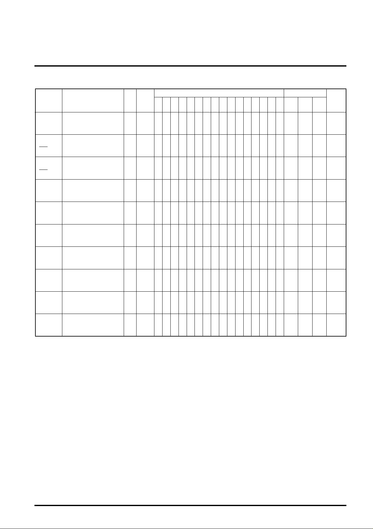
DESCRIPTION OF PIN
Pin No. Name Voltage and wave information Peripheral circuit of pins Description of function
The input impedance is
18kΩ. Add a bias to
outside as shown right
9V
2.4k
for use.
1
2
EXT AUDIO
IN
SOUND DET
COIL
3.25V
2.5V
4.7k
3.9k
25k
25k
0.01µF
30p
10k
20p
5V
10k
18k
TV (Without Y-DL)
TV (With Y-DL)
EXT (With Y-DL)
2.4k
4.5V2k
The FM detector is a
10k
quadrature detector and
externally connects a
tank coil or discriminator.
10k
This is also used as an
5p
3V
AV switching pin to apply
voltagethrougha 10kΩ.
GND to EXT (Y-DL)
OPEN to TV (Y-DL)
Vcc (5V) to TV (S input)
Sound direct output pin.
For de-emphasis,connect
a capacitor between this
2.4k
pin and GND.
3
SOUND DET
OUT
(Varying with coil position)
3.75V
18k
2.4k
4.5V2k
Sound output pin through
ATT.
23k
4
AF OUT
4.2V
9k
5.0V
Page 20

MITSUBISHI ICs (TV)
M52335SP
NTSC SYSTEM SINGLE-CHIP COLOR TV SIGNAL PROCESSOR
DESCRIPTION OF PIN (cont.)
Pin No. Name Voltage and wave information Peripheral circuit of pins Description of function
Dynamic AGC circuit is
used to improve AGC
response characteristics.
Set a filter constant to
avoid a sag around
5
IF AGC
FILTER
4.4 to 1.5V
1k
7.5k
70dBµ.
IF AGC Voltage
4.4V
50dBµ 70dBµ 100dBµ
IF Input
RFAGC delay point is set
by the voltage applied to
this pin.
1k
6
7
RF AGC
DELAY ADJ.
2k
GND-1
(VIF SIF)
Input resistance is 1kΩ.
Input capacitance is 7pF.
8
9
VIF IN
1.5V
80
1.2k
1.2k
320320
1.5V
10
VCC-1
(VIF SIF)
5V
11
Pin
Output
fc frequency
The f characteristic of a
loop in the locked state
11
APC FILTER
3V
can be set by R.
14k
R
3V
60p
3.4k
Normally, set fc in the
range of 100 to 150kHz.
3.4k
V11
fo
IF frequency
Page 21

MITSUBISHI ICs (TV)
j
j
M52335SP
NTSC SYSTEM SINGLE-CHIP COLOR TV SIGNAL PROCESSOR
DESCRIPTION OF PIN (cont.)
Pin No. Name Voltage and wave information Peripheral circuit of pins Description of function
12
13
H. VCC
AFC FILTER
6.25V
24k
3k
R
6.25V
Powersupplypinforhorizontal
and
v
erticalsystems.Itscurrent
is about 34mA
Horizontal AFC filter pin.
Action against VCR
skews can be taken by
increasing an external
resistor R to provide a
faster response speed.
However, horizontal
itters in a weak electric
field will increase.
.
Flyback pulse is sliced
on 4V to generate an
AFC2 detector pulse.
100
Remember that any peak
around 4V may cause
itters. The screen moves
rightward by integrating
14
AFC FBP IN
FBP
4V
1.35k
and entering the flyback
pulse.
CSB500F18 is used.
300 300
300
15
32fH OSC
3.8V
500F18
2kCSB
300
Applying voltage of 0.7V
or more operates the X-
2k1.2k
16
X-RAY
PROTECT
2k2k
1.2k
ray protector. Connect to
GND if not using the pin.
Page 22

MITSUBISHI ICs (TV)
f
M52335SP
NTSC SYSTEM SINGLE-CHIP COLOR TV SIGNAL PROCESSOR
DESCRIPTION OF PIN (cont.)
Pin No. Name Voltage and wave information Peripheral circuit of pins Description of function
Voltage goes up if a sync
signal is entered and
horizontal AFC is locked;
otherwise, the voltage
goes down. Therefore,
17
COINCIDENCE
OUT
8V (Synchronous)
to
0V (Asynchronous)
1k
the pin can be also used
as a MUTE detector. At
that time, pay attention to
high impedance.
Pulse as shown below is
output.
60k
18
19
V.OUT
VCC-2 (VCJ)
9V
30k
Power supply
RF AGC and SIF DET.
V
8.2V
0V
10H
or VC,AFT,
Horizontal pulse of 24µs
wide is output. It is open
2k200
20
H. OUT
200
33k
emitter output.
3.8V
0V
Color control pin. Its
voltage goes to 0V when
service SW is ON.
5.6k 640
21
COLOR
CONT.
4.5V
200
10k
4.5V
Service SW
Page 23

MITSUBISHI ICs (TV)
M52335SP
NTSC SYSTEM SINGLE-CHIP COLOR TV SIGNAL PROCESSOR
DESCRIPTION OF PIN (cont.)
Pin No. Name Voltage and wave information Peripheral circuit of pins Descripition of function
Video output pin. When a
flyback pulse is entered
10k 200
600
30k
22
-Y OUT
10k
2k
1k
60
for blanking from outside,
a blanking pulse is
entered internally and a
chroma symbol is also
blanked. The blanking
threshold voltage is 7.1V.
Open emitter output with
maximum current of
about 5mA.
23
24
25
R-Y OUT
G-Y OUT
B-Y OUT
5.4V
Input impedance is
50kΩ. Apply voltage of
2.5V or more when
inserting a character
signal.
26
27
28
OSD B
OSD G
OSD R
Vth
2.5V
300
50k
Tint control pin.
12k
29
TINT CONT.
4.5V
2k
4.5V
Page 24

MITSUBISHI ICs (TV)
M52335SP
NTSC SYSTEM SINGLE-CHIP COLOR TV SIGNAL PROCESSOR
DESCRIPTION OF PIN (cont.)
Pin No. Name Voltage and wave information Peripheral circuit of pins Description of function
Applying voltage of 2.5V
or more causes blanking.
30
FAST BLK IN
Vth
2.5V
300
0V
50k
Cap challenge is
changed by R. As R is
decreased, the cap
challenge becomes
narrower but phase jitters
are reduced.
4k
31
APC FILTER
6.5V
R
666666
Use XTAL of series
capacitance type.
300300
1k
32
CHROMA
OSC
6.8V
1k
Such as M351T01
3p
1k
As R is decreased,
chroma output increases
VCC
R
33
ACC FILTER
2k
1.6k
but ACC is not activated
smoothly.
3k
22k
Page 25

MITSUBISHI ICs (TV)
M52335SP
NTSC SYSTEM SINGLE-CHIP COLOR TV SIGNAL PROCESSOR
DESCRIPTION OF PIN (cont.)
Pin No. Name Voltage and wave information Peripheral circuit of pins Descripition of function
Pin holding the most
dark part of a video
signal. As R is increased,
R
34
BLACK
HOLD
About 3.2V
1.5k1.5k
the black peak is held;
contrarily, the peak gets
closer to an average.
3751.15k
2k
To decrease killer
sensitivity, connect a
several M of resistor
between the pin and
4.7k
35
KILLER
FILTER
7.6V at signal input
3.2k1.7kR
GND.
Can be controlled by
5.1V center.
40k
36
CONTRAST
CONT.
Normally 4.8V Applied
from outside
5k
200
20k
37
GND-2
(VCD)
Chroma signal standard.
Make an entry at
P-P. This pin is also
100
30p
200mV
used as a brightness
control pin. DC
20k
38
CHROMA IN/
BRIGHTNESS
4.5V
20k
33p
40k
4.5V
670
reproduction ratio is
100%.
Page 26

MITSUBISHI ICs (TV)
M52335SP
NTSC SYSTEM SINGLE-CHIP COLOR TV SIGNAL PROCESSOR
DESCRIPTION OF PIN (cont.)
Pin No. Name Voltage and wave information Peripheral circuit of pins Description of function
Used to connect a hold
capacitor.
3.9k 1k
39
PEDESTAL
CLAMP
About 2.2V
1.07k
1.4k 1.2k
Sharpness control pin.By
increasing voltage, the
1.5k
15k
10k
40
VIDEO TONE
CONT.
4.5V
6.2k
4.5V
pin is set to soft side.
Make an entry at low
input impedance to avoid
pedestal clamp.
Standard coupling
capacitor is 0.1µF. Make
an entry at 0.5VP-P.
41
42
Y IN
EXT VIDEO
IN
3.3V
39k
39k
5V
Make an entry at 1V
5k
150
P-P.
Page 27

MITSUBISHI ICs (TV)
cs
M52335SP
NTSC SYSTEM SINGLE-CHIP COLOR TV SIGNAL PROCESSOR
DESCRIPTION OF PIN (cont.)
Pin No. Name Voltage and wave information Peripheral circuit of pins Description of function
Output at 1.5VP-P.
43
Y SW OUT
2.5V
1.125k
eparationof emitter
Syn
input type. Vertical sync
separation is done inside
the IC.
1k
44
SYNC IN
6.6V
7.35V
Make an entry at 1VP-P.
150
45
TV IN
2.5V
20k
2.5V
Referencetuning
capacitance is 27pF. As
the capacitance is
850
850
decrease, the variable
range becomes wider but
46
47
VCO COIL
4V
stability becomes worse.
Page 28

MITSUBISHI ICs (TV)
M52335SP
NTSC SYSTEM SINGLE-CHIP COLOR TV SIGNAL PROCESSOR
DESCRIPTION OF PIN (cont.)
Pin No. Name Voltage and wave information Peripheral circuit of pins Description of function
Volume control pin.
20p
15k
48
SIF IN/ATT
4.5V
10k
29.3p
10k
2.4k
4.5V
Applying voltage of 2.5V
or more defeats AFT.
49
AFT
DEFEAT
23.3k
10k
Current output type. As
load resistor R is
increased, detector
sensitivity becomes
R
50
AFT OUT
8.2 to 0.5V
R
1k
higher but offlot becomes
larger.
Output at 1.4VP-P. 1.75V
is applied to sink tip.
7.5k
51
VIDEO OUT
12.5k
32.5k
2.7k 250
Page 29

MITSUBISHI ICs (TV)
M52335SP
NTSC SYSTEM SINGLE-CHIP COLOR TV SIGNAL PROCESSOR
DESCRIPTION OF PIN (cont.)
Pin No. Name Voltage and wave information Peripheral circuit of pins Description of function
Current output type.
Max. 0.4mA.
0.4mA
52
RF AGC OUT
50
0.4mA
 Loading...